

Standard Microsystems Corporation FDC37N869 Datasheet

FDC37N869
100 Pin TQFP Package
5V and 3.3V Super I/O Controller with Infrared Support for
Portable Applications
FEATURES
§ PC 99 Compliant
§ 5 Volt and 3.3 Volt Operation
§ Intelligent Auto Power Management
§ 16 Bit Address Qualification
§ 2.88MB Super I/O Floppy Disk Controller
- Licensed CMOS 765B Floppy Disk Controller
- Software and Register Compatible with
SMSC’s Proprietary 82077AA Compatible
Core
- Supports One Floppy Drive Directly
- Configurable Open Drain/Push-Pull Output
Drivers
- Supports Vertical Recording Format
- 16 Byte Data FIFO
- 100% IBM Compatibility
- Detects All Overrun and Underrun Conditions
- Sophisticated Power Control Circuitry (PCC)
Including Multiple Power-Down Modes for
Reduced Power Consumption
- DMA Enable Logic
- Data Rate and Drive Control Registers
- Swap Drives A and B
- Non-Burst Mode DMA Option
- 48 Base I/O Address, 15 IRQ and 4 DMA
Options
- Forceable Write Protect and Disk Change
Controls
§ Floppy Disk Available on Parallel Port Pins
ACPI Compliant
§ Enhanced Digital Data Separator
- 2Mbps, 1 Mbps, 500 Kbps, 300 Kbps,
250 Kbps Data Rates
- Programmable Precompensation Modes
§ Serial Ports
- Two High Speed NS16C550 Compatible
UARTs with Send/Receive 16 Byte FIFOs
- Supports 230k and 460k Baud
- Programmable Baud Rate Generator
- Modem Control Circuitry
§ Infrared Communications Controller
- IrDA v1.1 (4Mbps), HPSIR, ASKIR, Consumer
IR Support
- 2 IR Ports
- 96 Base I/O Address, 15 IRQ Options and 4
DMA Options
§ Multi-Mode Parallel Port with ChiProtect
- Standard Mode
- IBM PC/XT, PC/AT, and PS/2 Compatible Bidirectional Parallel Port
- Enhanced Parallel Port (EPP) Compatible
- EPP 1.7 and EPP 1.9 (IEEE 1284 Compliant)
- Enhanced Capabilities Port (ECP)
Compatible (IEEE 1284 Compliant)
- Incorporates ChiProtect Circuitry for Protection
Against Damage Due to Printer Power-On
- 192 Base I/O Address, 15 IRQ and 4 DMA
Options
§ Game Port Select Logic
- 48 Base I/O Addresses
§ General Purpose Address Decoder
- 16-Byte Block Decode
SMSC DS – FDC37N869 11/09/2000
ORDERING INFORMATION
Order Number: FDC37N869TQFP

© 2000 STANDARD MICROSYSTEMS CORPORATION (SMSC)
80 Arkay Drive
Hauppauge, NY 11788
(631) 435-6000
FAX (631) 273-3123
Standard Microsystems is a registered trademark of Standard Microsystems Corporation, and SMSC, ChiProtect, SuperCell and Multi-Mode are
trademarks of Standard Microsystems Corporation. Product names and company names are the trademarks of their respective holders. Circuit
diagrams utilizing SMSC products are included as a means of illustrating typical applications; consequently complete information sufficient for
construction purposes is not necessarily given. Although the information has been checked and is believed to be accurate, no responsibility is
assumed for inaccuracies. SMSC reserves the right to make changes to specifications and product descriptions at any time without notice. Contact
your local SMSC sales office to obtain the latest specifications before placing your product order. The provision of this information does not convey
to the purchaser of the semiconductor devices described any licenses under the patent rights of SMSC or others. All sales are expressly conditional
on your agreement to the terms and conditions of the most recently dated version of SMSC's standard Terms of Sale Agreement dated before the
date of your order (the "Terms of Sale Agreement"). The product may contain design defects or errors known as anomalies which may cause the
product's functions to deviate from published specifications. Anomaly sheets are available upon request. SMSC products are not designed,
intended, authorized or warranted for use in any life support or other application where product failure could cause or contribute to personal injury or
severe property damage. Any and all such uses without prior written approval of an Officer of SMSC and further testing and/or modification will be
fully at the risk of the customer. Copies of this document or other SMSC literature, as well as the Terms of Sale Agreement, may be obtained by
visiting SMSC’s website at http://www.smsc.com.
SMSC DISCLAIMS AND EXCLUDES ANY AND ALL WARRANTIES, INCLUDING WITHOUT LIMITATION ANY AND ALL IMPLIED WARRANTIES OF
MERCHANTABILITY, FITNESS FOR A PARTICULAR PURPOSE, TITLE, AND AGAINST INFRINGEMENT, AND ANY AND ALL WARRANTIES
ARISING FROM ANY COURSE OF DEALING OR USAGE OF TRADE.
IN NO EVENT SHALL SMSC BE LIABLE FOR ANY DIRECT, INCIDENTAL, INDIRECT, SPECIAL, PUNITIVE, OR CONSEQUENTIAL DAMAGES;
OR FOR LOST DATA, PROFITS, SAVINGS OR REVENUES OF ANY KIND; REGARDLESS OF THE FORM OF ACTION, WHETHER BASED ON
CONTRACT; TORT; NEGLIGENCE OF SMSC OR OTHERS; STRICT LIABILITY; BREACH OF WARRANTY; OR OTHERWISE; WHETHER OR NOT
ANY REMEDY IS HELD TO HAVE FAILED OF ITS ESSENTIAL PURPOSE, AND WHETHER OR NOT SMSC HAS BEEN ADVISED OF THE
POSSIBILITY OF SUCH DAMAGES.
SMSC DS – FDC37N869 Page 2 Rev. 11/09/2000

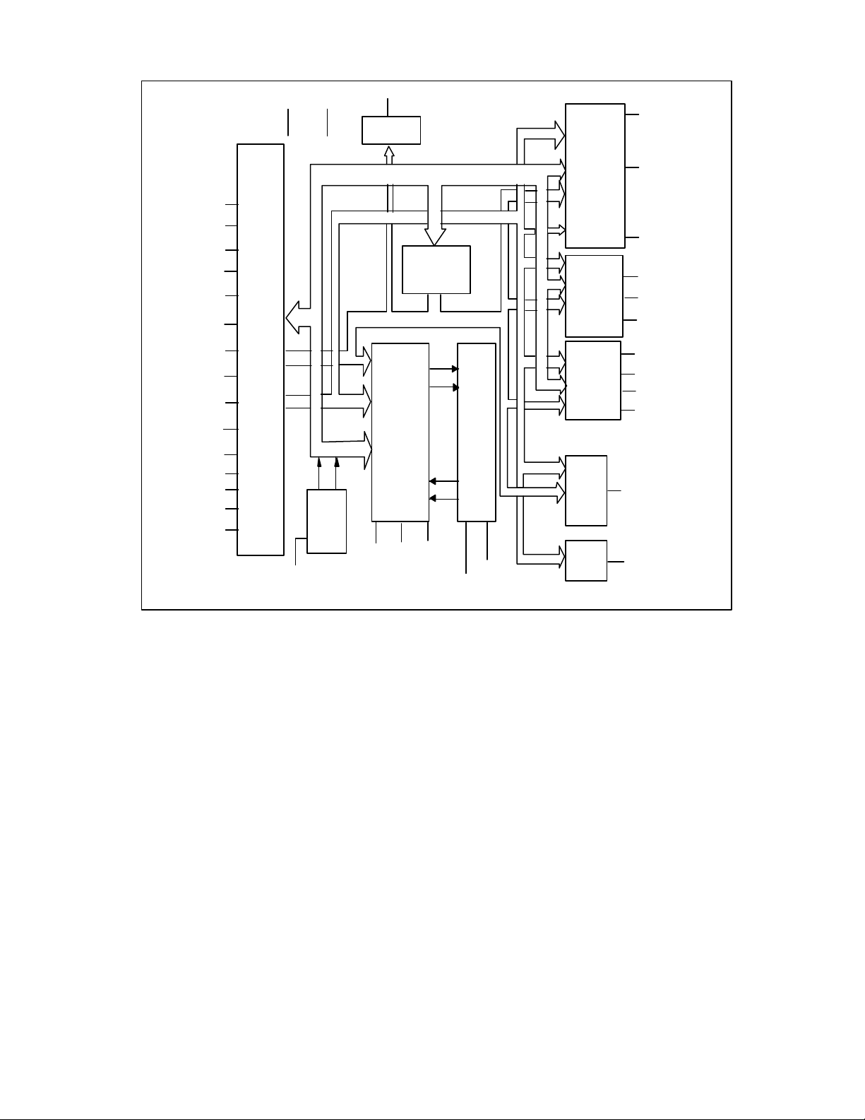
GENERAL DESCRIPTION
The SMSC FDC37N869 is a 5v/3.3v PC 99-compliant Super I/O Controller with Infrared support. The FDC37N869
utilizes SMSC’s proven SuperCell technology and is optimized for motherboard applications. The FDC37N869
incorporates SMSC’s true CMOS 765B floppy disk controller, advanced digital data separator, 16-byte data FIFO,
two 16C550 compatible UARTs, one Multi-Mode parallel port with ChiProtect circuitry plus EPP and ECP support,
game port chip select logic and one floppy direct drive support. The FDC37N869 does not require any external
filter components, is easy to use and offers lower system cost and reduced board area. The FDC37N869 is
software and register compatible with SMSC’s proprietary 82077AA core.
The true CMOS 765B core provides 100% compatibility with IBM PC/XT and PC/AT architectures and provides data
overflow and underflow protection. The SMSC advanced digital data separator incorporates SMSC’s patented data
separator technology allowing for ease of testing and use. The FDC37N869 supports both 1Mbps and 2Mbps data
rates and vertical recording operation at 1Mbps Data Rate.
The FDC37N869 also features a full 16-bit internally decoded address bus, a Serial IRQinterface with PCI
nCLKRUN support, relocatable configuration ports and four DMA channel options.
Both on-chip UARTs are compatible with the NS16C550. One UART includes additional support for a Serial
Infrared Interface that complies with IrDA v1.2 (Fast IR), HPSIR, and ASKIR formats (used by Sharp, Apple Newton,
and other PDAs), as well as Consumer IR.
The parallel port and the game port select logic are compatible with IBM PC/AT architectures. The parallel port
ChiProtect circuitry prevents damage caused by an attached powered printer when the FDC37N869 is not
powered.
The FDC37N869 incorporates sophisticated power control circuitry (PCC). The PCC supports multiple low power
down modes. The FDC37N869 also features Software Configurable Logic (SCL) for ease of use. SCL allows
programmable system configuration of key functions such as the FDC, parallel port, and UARTs.
SMSC DS – FDC37N869 Page 3 Rev. 11/09/2000

TABLE OF CONTENTS
GENERAL DESCRIPTION ...................................................................................................................3
PIN CONFIGURATION........................................................................................................................8
PIN DESCRIPTION.............................................................................................................................9
BUFFER TYPE PER PIN ..................................................................................................................9
BUFFER TYPE SUMMARY .................................................................................................................... 15
OUTPUT DRIVERS.............................................................................................................................. 15
FUNCTIONAL DESCRIPTION ............................................................................................................17
HOST PROCESSOR INTERFACE............................................................................................................. 17
FLOPPY DISK CONTROLLER ...........................................................................................................17
MODES OF OPERATION...................................................................................................................... 17
Floppy Modes........................................................................................................................... 17
Interface Modes......................................................................................................................... 18
FLOPPY DISK CONTROLLER INTERNAL REGISTERS .................................................................................... 18
STATUS REGISTER A (SRA)..................................................................................................... 18
STATUS REGISTER B (SRB)..................................................................................................... 21
DIGITAL OUTPUT REGISTER (DOR)........................................................................................... 23
TAPE DRIVE REGISTER (TDR) .................................................................................................. 24
MAIN STATUS REGISTER (MSR).............................................................................................. 25
DATA RATE SELECT REGISTER (DSR) .................................................................................... 26
DATA REGISTER (FIFO) ............................................................................................................29
DIGITAL INPUT REGISTER (DIR)................................................................................................ 29
CONFIGURATION CONTROL REGISTER (CCR).......................................................................... 31
STATUS REGISTER ENCODING.............................................................................................................. 32
RESET............................................................................................................................................ 33
RESET Pin (Hardware Reset)..................................................................................................... 34
DOR Reset vs. DSR Reset (Software Reset)................................................................................. 34
DMA TRANSFERS............................................................................................................................. 34
CONTROLLER PHASES ....................................................................................................................... 34
Command Phase........................................................................................................................ 34
Execution Phase ....................................................................................................................... 34
Result Phase ............................................................................................................................. 35
COMMAND SET/DESCRIPTIONS ............................................................................................................. 36
INSTRUCTION SET.............................................................................................................................. 38
DATA TRANSFER COMMANDS.............................................................................................................. 46
Read Data ................................................................................................................................. 46
Read Deleted Data .....................................................................................................................48
Read A Track............................................................................................................................ 48
Write Data .................................................................................................................................49
Write Deleted Data .................................................................................................................... 50
Verify......................................................................................................................................... 50
Format A Track .........................................................................................................................51
CONTROL COMMANDS ....................................................................................................................... 52
Read ID .....................................................................................................................................52
Recalibrate................................................................................................................................ 52
Seek ......................................................................................................................................... 53
Sense Interrupt Status ................................................................................................................ 53
Sense Drive Status ....................................................................................................................54
Specify ..................................................................................................................................... 54
SMSC DS – FDC37N869 Page 4 Rev. 11/09/2000

Configure.................................................................................................................................. 54
Version..................................................................................................................................... 55
Relative Seek............................................................................................................................. 55
Perpendicular Mode.................................................................................................................. 56
LOCK........................................................................................................................................ 57
ENHANCED DUMPREG............................................................................................................. 57
COMPATIBILITY ............................................................................................................................ 57
PARALLEL PORT FLOPPY DISK CONTROLLER.......................................................................................... 57
SERIAL PORT (UART)...................................................................................................................... 59
REGISTER DESCRIPTION...................................................................................................................... 59
RECEIVE BUFFER REGISTER (RB)............................................................................................ 59
TRANSMIT BUFFER REGISTER (TB)......................................................................................... 59
INTERRUPT ENABLE REGISTER (IER)....................................................................................... 59
INTERRUPT IDENTIFICATION REGISTER (IIR) ............................................................................ 60
FIFO CONTROL REGISTER (FCR) ..............................................................................................62
LINE CONTROL REGISTER (LCR) ..............................................................................................63
MODEM CONTROL REGISTER (MCR)....................................................................................... 64
LINE STATUS REGISTER (LSR) ................................................................................................ 65
MODEM STATUS REGISTER (MSR).......................................................................................... 66
SCRATCHPAD REGISTER (SCR)............................................................................................... 67
PROGRAMMABLE BAUD RATE GENERATOR DIVISOR LATCHES ........................................... 67
The Affects of RESET on the UART Registers............................................................................ 68
FIFO INTERRUPT MODE OPERATION...................................................................................................... 68
FIFO POLLED MODE OPERATION......................................................................................................... 69
NOTES ON SERIAL PORT FIFO MODE OPERATION................................................................................... 70
GENERAL................................................................................................................................. 70
TX AND RX FIFO OPERATION ...................................................................................................71
INFRARED INTERFACE .................................................................................................................... 71
IRDA SIR/FIR AND ASKIR................................................................................................................ 71
CONSUMER IR.................................................................................................................................. 72
HARDWARE INTERFACE...................................................................................................................... 72
IR HALF DUPLEX TURNAROUND DELAY TIME........................................................................................... 72
PARALLEL PORT............................................................................................................................. 74
IBM XT/AT COMPATIBLE, BI-DIRECTIONAL AND EPP MODES ........................................................75
DATA PORT ..............................................................................................................................75
STATUS PORT ..........................................................................................................................75
CONTROL PORT ....................................................................................................................... 76
EPP ADDRESS PORT ................................................................................................................77
EPP DATA PORT 0.................................................................................................................... 77
EPP DATA PORT 1.................................................................................................................... 77
EPP DATA PORT 2.................................................................................................................... 77
EPP DATA PORT 3.................................................................................................................... 77
EPP 1.9 OPERATION .................................................................................................................... 77
Software Constraints .................................................................................................................78
EPP 1.9 Write ............................................................................................................................78
EPP 1.9 Read ............................................................................................................................ 78
EPP 1.7 OPERATION .................................................................................................................... 79
Software Constraints .................................................................................................................79
EPP 1.7 Write ............................................................................................................................79
EPP 1.7 Read ............................................................................................................................ 79
EXTENDED CAPABILITIES PARALLEL PORT.................................................................................. 81
Vocabulary ............................................................................................................................... 81
ISA IMPLEMENTATION STANDARD.......................................................................................... 82
SMSC DS – FDC37N869 Page 5 Rev. 11/09/2000

Description ............................................................................................................................... 82
Register Definitions................................................................................................................... 83
OPERATION.............................................................................................................................. 89
AUTO POWER MANAGEMENT ......................................................................................................... 93
FDC POWER MANAGEMENT ............................................................................................................... 93
DSR From Powerdown ..............................................................................................................93
Wake Up From Auto Powerdown.............................................................................................. 93
Register Behavior...................................................................................................................... 94
Pin Behavior............................................................................................................................. 94
UART POWER MANAGEMENT ............................................................................................................. 96
PARALLEL PORT.............................................................................................................................. 96
SERIAL IRQ .................................................................................................................................. 96
Introduction.............................................................................................................................. 96
IRQSER Cycle Modes................................................................................................................ 97
IRQSER IRQ/Data Frames.......................................................................................................... 98
Stop Cycle Control.................................................................................................................... 99
Latency..................................................................................................................................... 99
EOI/ISR Read Latency ............................................................................................................... 99
AC/DC Specification Issue .........................................................................................................99
Reset and Initialization ................................................................................................................99
ADD PCI NCLKRUN SUPPORT ....................................................................................................100
Overview.................................................................................................................................100
Using nCLKRUN ......................................................................................................................100
CONFIGURATION...........................................................................................................................101
CONFIGURATION ACCESS PORTS........................................................................................................101
CONFIGURATION STATE ....................................................................................................................102
Entering the Configuration State .............................................................................................102
Configuration Register Programming ......................................................................................102
Exiting the Configuration State...............................................................................................102
Programming Example ...........................................................................................................102
Configuration Select Register (CSR) ........................................................................................103
CONFIGURATION REGISTERS DESCRIPTION ............................................................................................103
CR00.......................................................................................................................................104
CR01.......................................................................................................................................104
CR02.......................................................................................................................................106
CR03.......................................................................................................................................106
CR04.......................................................................................................................................107
CR05.......................................................................................................................................108
CR06.......................................................................................................................................108
CR07.......................................................................................................................................109
CR08.......................................................................................................................................109
CR09.......................................................................................................................................109
CR0A ......................................................................................................................................110
CR0B ......................................................................................................................................110
CR0C ......................................................................................................................................111
CR0D ......................................................................................................................................111
CR0E ......................................................................................................................................111
CR0F.......................................................................................................................................111
CR10.......................................................................................................................................112
CR11.......................................................................................................................................112
CR12 - CR13 ............................................................................................................................112
CR14.......................................................................................................................................113
CR15.......................................................................................................................................113
CR16.......................................................................................................................................113
SMSC DS – FDC37N869 Page 6 Rev. 11/09/2000

CR17.......................................................................................................................................113
CR18 - CR1D ...........................................................................................................................114
CR1E ......................................................................................................................................114
CR1F.......................................................................................................................................114
CR20.......................................................................................................................................115
CR21.......................................................................................................................................115
CR23.......................................................................................................................................115
CR24.......................................................................................................................................116
CR25.......................................................................................................................................116
CR26.......................................................................................................................................116
CR27.......................................................................................................................................117
CR28.......................................................................................................................................117
CR29.......................................................................................................................................118
CR2A ......................................................................................................................................118
CR2B ......................................................................................................................................118
CR2C ......................................................................................................................................118
CR2D ......................................................................................................................................119
CR2E ......................................................................................................................................119
CR2F.......................................................................................................................................119
OPERATIONAL DESCRIPTION .......................................................................................................120
MAXIMUM GUARANTEED RATINGS .............................................................................................120
DC ELECTRICAL CHARACTERISTICS ...........................................................................................120
AC TIMING.....................................................................................................................................126
HOST TIMING..................................................................................................................................126
FDD TIMING ..................................................................................................................................130
SERIAL PORT TIMING .......................................................................................................................131
PARALLEL PORT TIMING...................................................................................................................136
Parallel Port EPP Timing .........................................................................................................137
Parallel Port ECP Timing.........................................................................................................142
PACKAGE OUTLINES ..................................................................................................................... 146
FDC37N869 REVISIONS .................................................................................................................147
SMSC DS – FDC37N869 Page 7 Rev. 11/09/2000
IRMODE/IRRX3
RXD1
TXD1
nDSR1
nRTS1
nCTS1
nDTR1
nRI1
nDCD1
nRI2
nDCD2
RXD2
TXD2
nDSR2
nRTS2
nCTS2
nDTR2
nADRX/nCLKRUN
VSS
nDACK_C
A10
IRQIN
DRQ_C
IOCHRDY
DRVDEN0
nMTR0
76
77
78
79
80
81
82
83
84
85
86
87
88
89
90
91
92
93
94
95
96
97
98
99
100
nSTROBE
nAUTOFD
nERROR
75
74
73
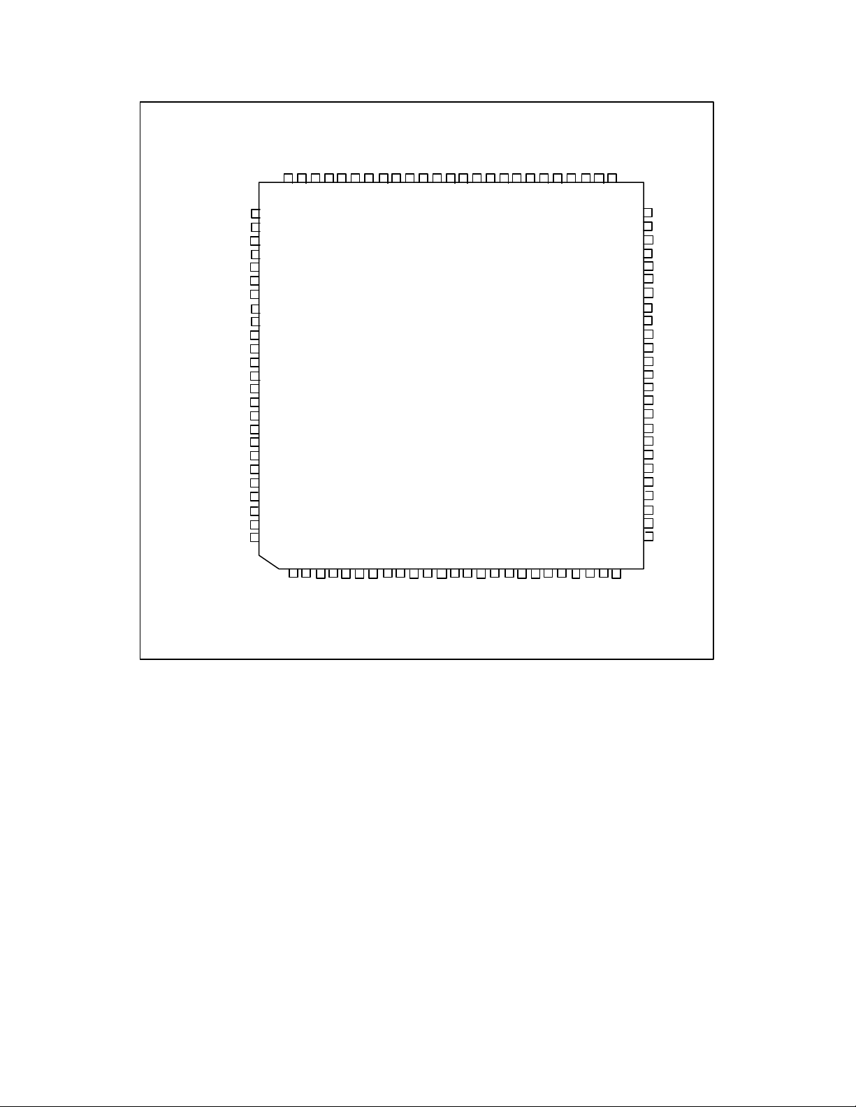
PIN CONFIGURATION
nINIT
nSLCT
VCC
PD0
PD1
PD2
PD3
VSS
PD4
PD5
PD6
PD7
nACK
BUSYPESLCT
72
71
70
69
68
67
66
65
64
63
62
61
60
59
58
57
FDC37N869
100 PIN TQFP
PWRGD
RESET_DRV
D7D6D5
56
55
54
53
52
D4
51
50
49
48
47
46
45
44
43
42
41
40
39
38
37
36
35
34
33
32
31
30
29
28
27
26
DRQ_B
D3
D2
D1
D0
VSS
AEN
nIOW
nIOR
A9
A8
A7
CLK33
SIRQ
A12
A11
nDACK_B
TC
A6
A5
A4
A3
A2
A1
A0
1 2 3
4
5
6
7
8
9
10
11
12
13
14
15
16
17
18
A13
A14
nDS0
VSS
nDIR
nSTEP
nWDATA
nHDSEL
nWGATE
nTRK0
nINDEX
VCC
nRDATA
nWRTPRT
DRQ_D
DRVDEN1
nDSKCHG
CLK14
FIGURE 1 - FDC37N869 PIN CONFIGURATION
19
20
DRQ_A
nDACK_A
21
22 2324
nDACK_D
IRTX2
IRRX2
25
A15
SMSC DS – FDC37N869 Page 8 Rev. 11/09/2000

PIN DESCRIPTION
BUFFER TYPE PER PIN
Table 1 - DESCRIPTION OF PIN FUNCTIONS
TQFP
PIN # NAME SYMBOL
46-49
Data Bus 0-7D0-D7 IO12 The data bus connection used by the host
51-54
42 nI/O Read nIOR IS This active low signal is issued by the host
43 nI/O Write nIOW IS This active low signal is issued by the host
44 Address
AEN IS Active high Address Enable indicates DMA
Enable
26-32
39-41,
Address
Bus
A0-A15 I These host address bits determine the I/O
95,35,
36,1,
3,25
19,50,
97,17
DMA
Request
A, B, C, D
DRQ_A
DRQ_B
DRQ_C
DRQ_D
20,34,
94,22
nDMA
Acknowledge
A, B, C, D
33 Terminal
nDACK_A
nDACK_B
nDACK_C
nDACK_D
TC IS This signal indicates that DMA data transfer is
Count
37 Serial IRQ SIRQ IO12 Serial IRQ pin used with the CLK33 pin to
38 PCI Clock CLK33 ICLK 33MHz PCI clock input, used with the SIRQ and
55 Reset RESET_
DRV
98 I/O Channel
IOCHRDY OD12 This pin is pulled low to extend the read/write
Ready
(Note4)
14 nRead Disk
nRDATA IS Raw serial bit stream from the disk drive, low
Data
BUFFER
6
MODE
DESCRIPTION
HOST PROCESSOR INTERFACE
microprocessor to transmit data to and from the
chip. These pins are in a high-impedance state
when not in the output mode.
microprocessor to indicate an I/O read
operation.
microprocessor to indicate an I/O write
operation.
operations on the host data bus. Used internally
to qualify appropriate address decodes.
address to be accessed during nIOR and nIOW
cycles. These bits are latched internally by the
leading edge of nIOR and nIOW. All internal
address decodes use the full A0 to A15 address
bits.
O12 These active high outputs are the DMA request
for byte trans fers of data between the host and
the chip. These signals are cleared on the last
byte of the data transfer by the nDACK signal
going low (or by nIOR going low if nDACK was
already low as in demand mode).
IS These are active low inputs acknowledging the
request for a DMA transfer of data between the
host and the chip. These inputs enable the DMA
read or write internally.
complete. TC is only accepted when nDACK_x
is low. In AT and PS/2 model 30 modes, TC is
active high and in PS/2 mode, TC is active low.
transfer FDC37N869 interrupts to the host.
the nCLKRUN pins to serially transfer
FDC37N869 interrupts to the host.
IS This active high signal resets the chip and must
be valid for 500ns minimum. The effect on the
internal registers is described in the appropriate
section. The configuration registers are not
affected by this reset.
command. IOCHRDY can used by the IRCC and
by the Parallel Port in EPP mode.
FLOPPY DISK INTERFACE
active. Each falling edge represents a flux
transition of the encoded data.
SMSC DS – FDC37N869 Page 9 Rev. 11/09/2000

TQFP
PIN # NAME SYMBOL
8 nWrite
nWGATE (O12/
Gate
BUFFER
MODE
OD12)
6
DESCRIPTION
This active low high current driver allows current
to flow through the write head. It becomes active
just prior to writing to the diskette.
7 nWrite
Data
nWDATA (O12/
OD12)
This active low high current driver provides the
encoded data to the disk drive. Each falling
edge causes a flux transition on the media.
9 nHead
Select
nHDSEL (O12/
OD12)
This high current output selects the floppy disk
side for reading or writing. A logic “1” on this pin
means side 0 will be accessed, while a logic “0”
means side 1 will be accessed.
5 Direction
Control
nDIR (O12/
OD12)
This high current low active output determines
the direction of the head movement. A logic “1”
on this pin means outward motion, while a logic
“0” means inward motion.
6 nStep Pulse nSTEP (O12/
OD12)
This active low high current driver issues a low
pulse for each track-to-track movement of the
head.
15 Disk
Change
nDSKCHG IS This input senses that the drive door is open or
that the diskette has possibly been changed
since the last drive selection. This input is
inverted and read via bit 7 of I/O address 3F7H.
The nDSKCHG bit also depends upon the state
of the Force Disk Change bits in the Force FDD
Status Change configuration register (see
section CR17 on page 109).
2 nDrive
Select 0
100 nMotor On 0 nMTR0 (O12/
nDS0 (O12/
OD12)
Active low output selects drive 0.
These active low output selects motor drive 0.
OD12)
99 Drive
Density 0
12 nWrite
Protected
DRVDEN0 (O12/
OD12)
Indicates the drive and media selected. Refer to
configuration registers CR03, CR0B, CR1F.
nWRTPRT IS This active low Schmitt Trigger input senses
from the disk drive that a disk is write protected.
Any write command is ignored. The nWRPRT bit
also depends upon the state of the Force Write
Protect bit in the Force FDD Status Change
configuration register (see section CR17 on
page 109).
11 wTrack 00 nTRK0 IS This active low Schmitt Trigger input senses
from the disk drive that the head is positioned
over the outermost track.
10 nIndex nINDEX IS This active low Schmitt Trigger input senses
from the disk drive that the head is positioned
over the beginning of a track, as marked by an
index hole.
16 Drive
Density 1
DRVDEN 1 (O12/
OD12)
Indicates the drive and media selected. Refer to
configuration registers CR03, CR0B, CR1F.
SERIAL PORTS INTERFACE
86 Receive
Data 2
87 Transmit
Data 2
RXD2 IS Receiver serial data input for port 2. IR Receive
Data
TXD2 O12PD Transmit serial data output for port 2. IR
transmit data.
(Note5)
76 Receive
RXD1 I Receiver serial data input for port 1.
Data 1
SMSC DS – FDC37N869 Page 10 Rev. 11/09/2000

TQFP
PIN # NAME SYMBOL
77 Transmit
TXD1 O12 Transmit serial data output for port 1.
Data 1
79,89 nRequest to
nRTS1
Send
nRTS2
(System
(SYSOPT)
Option)
81,91 nData
nDTR1
Terminal
Ready
80,90 nClear to
nDTR2
nCTS1
Send
nCTS2
78,88 nData Set
nDSR1
Ready
nDSR2
83,85 nData
nDCD1
Carrier
Detect
nDCD2
BUFFER
6
MODE
DESCRIPTION
O6 Active low Request to Send outputs for the Serial
Port. Handshake output signal notifies modem
that the UART is ready to transmit data. This
signal can be programmed by writing to bit 1 of
the Modem Control Register (MCR). The
hardware reset will reset the nRTS signal to
inactive mode (high). nRTS is forced inactive
during loop mode operation.
At the trailing edge of hardware reset the nRTS2
inputs is latched to determine the configuration
base address: 0 = INDEX Base I/O Address 3F0
Hex; 1 = INDEX Base I/O Address 370 Hex.
O6 Active low Data Terminal Ready outputs for the
serial port. Handshake output signal notifies
modem that the UART is ready to establish data
communication link. This signal can be
programmed by writing to bit 0 of Modem Control
Register (MCR). The hardware reset will reset
the nDTR signal to inactive mode (high). nDTR
is forced inactive during loop mode operation.
I Active low Clear to Send inputs for the serial port.
Handshake signal which notifies the UART that
the modem is ready to receive data. The CPU
can monitor the status of nCTS signal by reading
bit 4 of Modem Status Register (MSR). A nCTS
signal state change from low to high after the
last MSR read will set MSR bit 0 to a 1. If bit 3 of
the Interrupt Enable Register is set, the interrupt
is generated when nCTS changes state. The
nCTS signal has no effect on the transmitter.
Note: Bit 4 of MSR is the complement of nCTS.
I Active low Data Set Ready inputs for the serial
port. Handshake signal which notifies the UART
that the modem is ready to establish the
communication link. The CPU can monitor the
status of nDSR signal by reading bit 5 of Modem
Status Register (MSR). A nDSR signal state
change from low to high after the last MSR read
will set MSR bit 1 to a 1. If bit 3 of Interrupt
Enable Register is set, the interrupt is generated
when nDSR changes state. Note: Bit 5 of MSR
is the complement of nDSR.
I Active low Data Carrier Detect inputs for the
serial port. Handshake signal which notifies the
UART that carrier signal is detected by the
modem. The CPU can monitor the status of
nDCD signal by reading bit 7 of Modem Status
Register (MSR). A nDCD signal state change
from low to high after the last MSR read will set
MSR bit 3 to a 1. If bit 3 of Interrupt Enable
Register is set, the interrupt is generated when
nDCD changes state. Note: Bit 7 of MSR is the
complement of nDCD.
SMSC DS – FDC37N869 Page 11 Rev. 11/09/2000

TQFP
PIN # NAME SYMBOL
82,84 nRing
nRI1
Indicator
nRI2
BUFFER
MODE
I
(Note1)
6
DESCRIPTION
Active low Ring Indicator inputs for the serial
port. Handshake signal which notifies the UART
that the telephone ring signal is detected by the
modem. The CPU can monitor the status of nRI
signal by reading bit 6 of Modem Status Register
(MSR). A nRI signal state change from low to
high after the last MSR read will set MSR bit 2 to
a 1. If bit 3 of Interrupt Enable Register is set,
the interrupt is generated when nRI changes
state. Note: Bit 6 of MSR is the complement of
nRI.
TQFP
PIN # NAME SYMBOL
71 nPrinter
nSLCT
Select
Input/FDC
nStep
Pulse
(Note3)
72 nInitiate
nSTEP
nINIT
Output/
FDC
nDirection
Control
(Note3)
74 nAutofeed
nDIR
nAUTOFD
Output/
FDC
nDensity
Select
(Note3)
nDENSEL
75 nStrobe
nSTROBE
Output/
FDC
nDrive
Select 0
(Note3)
nDS0
59 Busy/
BUSY
FDC
nMotor On
1
nMTR1
BUFFER
6
MODE
DESCRIPTION
PARALLEL PORT INTERFACE (NOTE 2)
(OD14/OP14)/OD12 This active low output selects the printer.
This is the complement of bit 3 of the
Printer Control Register.
Refer to Parallel Port description for use
of this pin in ECP and EPP mode.
See FDC Pin definition.
(OD14/OP14)/OD12 This output is bit 2 of the printer control
register. This is used to initiate the printer
when low.
Refer to Parallel Port description for use
of this pin in ECP and EPP mode.
See FDC Pin definition.
(OD14/OP14)/OD12 This output goes low to cause the printer
to automatically feed one line after each
line is printed. The nAUTOFD output is
the complement of bit 1 of the Printer
Control Register.
Refer to Parallel Port description for use
of this pin in ECP and EPP mode.
See FDC Pin definition.
(OD14/OP14)/OD12 An active low pulse on this output is used
to strobe the printer data into the printer.
The nSTROBE output is the complement
of bit 0 of the Printer Control Register.
Refer to Parallel Port description for use
of this pin in ECP and EPP mode.
See FDC Pin definition.
I/OD12 This is a status output from the printer, a
high indicating that the printer is not ready
to receive new data. Bit 7 of the Printer
Status Register is the complement of the
BUSY input. Refer to Parallel Port
description for use of this pin in ECP and
EPP mode.
See FDC Pin definition.
SMSC DS – FDC37N869 Page 12 Rev. 11/09/2000

TQFP
PIN # NAME SYMBOL
60 nAcknowl-
nACK
edge/FDC
nDrive
Select 1
BUFFER
6
MODE
I/OD12 A low active output from the printer
indicating that it has received the data and
is ready to accept new data. Bit 6 of the
Printer Status Register reads the nACK
input. Refer to Parallel Port description for
nDS1
use of this pin in ECP and EPP mode.
See FDC Pin definition.
58 Paper End/
FDC
nWrite
Data
PE
I/OD12 Another status output from the printer, a
high indicating that the printer is out of
paper. Bit 5 of the Printer Status Register
reads the PE input. Refer to Parallel Port
description for use of this pin in ECP and
nWRDATA
EPP mode.
See FDC Pin definition.
57 Printer
Selected
Status/
FDC
nWrite
Gate
73 nError/FDC
nHead
Select
SLCT
nWGATE
nERROR
I/OD12 This high active output from the printer
indicates that it has power on. Bit 4 of the
Printer Status Register reads the SLCT
input. Refer to Parallel Port description for
use of this pin in ECP and EPP mode.
See FDC Pin definition.
I/OD12 A low on this input from the printer
indicates that there is a error condition at
the printer. Bit 3 of the Printer Status
register reads the nERR input. Refer to
Parallel Port description for use of this pin
nHDSEL
in ECP and EPP mode.
See FDC Pin definition.
69 Port Data
PD0
IOP14/IS Port Data 0
0/FDC
nIndex
68 Port Data
nINDEX
PD1
See FDC Pin definition.
IOP14/IS Port Data 1
1/FDC
nTrack 0
67 Port Data
nTRK0
PD2
See FDC Pin definition.
IOP14/IS Port Data 2
2/FDC
nWrite
nWRTPRT
See FDC Pin definition.
Protected
66 Port Data
PD3
IOP14/IS Port Data 3
3/FDC
nRead
nRDATA
See FDC Pin definition.
Disk Data
64 Port Data
PD4
IOP14/IS Port Data 4
4/FDC
nDisk
nDSKCHG
See FDC Pin definition.
Change
63 Port Data 5 PD5 IOP14 Port Data 5
62 Port Data
PD6
IOP14/ OD12 Port Data 6
6/FDC
nMotor On
nMTR0
See FDC Pin definition.
0
61 Port Data 7 PD7 IOP14 Port Data 7
DESCRIPTION
SMSC DS – FDC37N869 Page 13 Rev. 11/09/2000

TQFP
STBY
PIN # NAME SYMBOL
BUFFER
MODE
6
ALTERNATE IR PINS/MISC
18 14.318 MHz
Input Clock
CLK14 ICLK The external connection to a single source 14.318
MHz clock.
23 IR Receive 2 IRRX2 IS IR Receive input
DESCRIPTION
24 IR Transmit 2
IRTX2 O12PD IR transmit output
(Note5)
92 Address X/
PCI Clock
Controller
nADRX/
nCLKRU
N
OD12/
IOD12
The active-low address decoder output nADRX can
be asserted on 1, 8, or 16-byte address
boundaries (an external pull-up is required). Refer
to configuration registers CR03, CR08, and CR09
for more information. nCLKRUN is used to
indicate the PCI clock status and to request that a
stopped clock be started.
21 IR Mode/ IR
Receive 3
IRMODE/
IRRX3
O6/IS IR mode
IR Receive 3
56 Power Good/
nGame Port
Chip Select
PWRGD
I/O4 This active high input indicates that the power
(VCC) is valid. For device operation PWRGD must
be active. When PWRGD is inactive, all inputs are
disconnected and put into a low power mode; all
outputs are put into high impedance. The contents
of all registers are preserved as long as VCC is
valid. The output driver current drain when
PWRGD is inactive mode drops to I
current.
nGAMEC
S
This is the Game Port Chip Select output - active
low. It will go active when the I/O address, qualified
by AEN, matches that selected in Configuration
register CR1E.
96 External
Interrupt
IRQIN IS This pin is used to steer an interrupt signal from
an external device onto one of 15 IRQs.
Input
POWER INTERFACE
13,70 Power VCC Positive Supply Voltage. (5V or 3.3V)
4,45,
Ground VSS Ground Supply.
65,93
- standby
Note 1: nRI and the UART interrupts are active when PWRGD is active and the UARTS are either fully powered
or in AUTOPOWER DOWN mode.
Note 2: The FDD output pins multiplexed in the PARALLEL PORT INTERFACE are OD drivers only and are not
affected by the FDD Output Driver Controls (see section CR05 on page 108).
Note 3: Active (push-pull) output drivers are required on these pins in the enhanced parallel port
modes.
Note 4: An external pull-up must be provided for IOCHRDY.
Note 5: The pull-down on this pin is always active including when the output driver is tristated and regardless of
the state of PWRGD.
Note 6: Buffer Modes describe the pad driver properties per function. Buffer Modes on multiplexed pins are
separated by a slash “/”. For example, the Buffer Modes for a multiplexed pin with two functions where
the primary function is an input and the secondary function is an 8mA bidirectional driver is “I/IO8”.
Buffer Modes in parenthesis represent multiple Buffer Modes for a single pin function.
SMSC DS – FDC37N869 Page 14 Rev. 11/09/2000

Buffer Type Summary
Table 2 below describes the buffer types shown in Table 1. All values are specified at V
= +3.3v, ±10%
cc
Table 2 - FDC37N869 Buffer Type Summary (See Note)
BUFFER TYPE DESCRIPTION
IO12 Input/Output. 12mA sink; 6mA source
O12 Output. 12mA sink; 6mA source
O12PD Output. 12mA sink; 6mA source with 30µa pull-down
OD12 Open Drain. 12mA sink
O6 Output. 6mA sink; 3mA source
OD14 Open Drain. 14mA sink
OP14 Output. 14mA sink; 14mA source. Backdrive Protected
IOP14 Input/Output. 14mA sink; 14mA source. Backdrive Protected
O4 Output. 4mA sink; 2mA source
ICLK Input to Crystal Oscillator Circuit (TTL levels)
I Input TTL Compatible
IS Input with Schmitt Trigger
IOD12 Input/Open Drain Output. 12mA sink
Note: These are minimum ratings guaranteed at 5V and 3.3V.
Output Drivers
Active output drivers in the FDC37N869 will always achieve the minimum specified DC Electrical Characteristics
shown in Table 120.
Note: If there is a pull-up on an external node driven by an active output driver the FDC37N869 may sink current
from the pull-up through the low impedance source.
SMSC DS – FDC37N869 Page 15 Rev. 11/09/2000
TXD1, nCTS1, nRTS1,
nWGATE
nCS
nIOR
nIOW
AEN
A0-A15
D0-D7
DRQ_A-D
nDACK_A-D
SIRQ
CLK33
nADRX/nCLKRUN
RESET
IRQIN
IOCHRDY
TC
HOST
CPU
INTERFACE
Vcc (2)
14.318
CLOCK
Vss (4)
CLOCK
GEN
PWRGD/nGAMECS
POWER
MANAGEMENT
ADDRESS BUS
SMSC
PROPRIETARY
82077
COMPATIBLE
VERTICAL
FLOPPYDISK
CONTROLLER
CORE
nINDEX
nDIR
nTRK0
nSTEP
nDSKCHG
DRVDEN0
nWRPRT
DRVDEN1
DATA BUS
CONFIGURATION
REGISTERS
CONTROL BUS
WDATA
WCLOCK
RCLOCK
RDATA
nDS0
nMTR0
nHDSEL
nWDATA
DIGITAL
DATA
SEPARATOR
WITH WRITE
PRECOM-
PENSATION
nRDATA
MULTI-MODE
PARALLEL
PORT/FDC
MUX
16C550
COMPATIBLE
SERIAL
PORT 1
16C550
COMPATIBLE
SERIAL
PORT 2 WITH
INFRARED
IR
GAME
PORT
DECODER
nSLCTIN/nSTEP,nINI
T/nDIR, nAUTOFD/
nDENSEL,
nSTROBE/nDS0,
BUSY/nMTR1,
nACK/nDS1,
PE/nWRDATA,nERR
OR/nHDSEL,
PD0/nINDEX,
PD1/nTRK0,
PD2/nWRTPRT,
PD3/nRDATA,
PD4/nDSKCHG,
PD6/nMTR,
PD5/
PD7
RXD1
nDSR1, nDCD1, nRI,
nDTR1
IR Mode/IRR3
TXD2/IRTX,nCTS2,
nRTS2
RXD2/IRRX
nDSR2,nDCD2,
nRI2,nDTR2
IRRX2, IRTX2
See Power Mgt
FIGURE 2 - FDC37N869 BLOCK DIAGRAM
SMSC DS – FDC37N869 Page 16 Rev. 11/09/2000

FUNCTIONAL DESCRIPTION
Super I/O Registers
Table 3 shows the addresses of the various device blocks of the Super I/O immediately after power up. The base
addresses must be set in the configuration registers before accessing these devices. The base addresses of the
FDC, Serial and Parallel Ports can be moved via the configuration registers.
Host Processor Interface
The host processor communicates with the FDC37N869 using the Super I/O registers. Register access is
accomplished through programmed I/O or DMA transfers. All registers are 8 bits wide. All host interface output
buffers are capable of sinking a minimum of 12 mA.
Table 3 - FDC37N869 Block Addresses
ADDRESS BLOCK NAME NOTES
3F0, 3F1 or 370, 371 Configuration Write only; Note 1
Base +[0:7] Floppy Disk Disabled at power up; Note 2
Base +[0:7] Serial Port Com 1 Disabled at power up; Note 2
Base1 +[0:7]
Base2 +[0:7]
Base +[0:3] all modes
Base +[4:7] for EPP
Base +[400:403] for ECP
Serial Port Com 2
Parallel Port Disabled at power up; Note 2
Disabled at power up; Note 2
Note 1: Configuration registers can only be modified in the configuration state, refer to section CONFIGURATION
on page 101 for more information. All logical blocks in the FDC37N869 can operate normally in the Configuration
State.
Note 2: The base addresses must be set in the configuration registers before accessing the logical device
blocks.
FLOPPY DISK CONTROLLER
The Floppy Disk Controller (FDC) provides the interface between a host microprocessor and the floppy disk drives.
The FDC integrates the functions of the Formatter/Controller, Digital Data Separator, Write Precompensation and
Data Rate Selection logic for an IBM XT/AT compatible FDC. The true CMOS 765B core guarantees 100% IBM PC
XT/AT compatibility in addition to providing data overflow and underflow protection.
The FDC37N869 is compatible with the 82077AA using SMSC’s proprietary floppy disk controller core. For
information about the floppy disk on the Parallel Port pins refer to section Parallel Port Floppy Disk Controller on
page 57.
Modes Of Operation
The FDC37N869 Floppy Disk Controller has two Floppy modes and three Interface modes. Each of the three
Interface modes are available in each of the two Floppy modes.
Floppy Modes
The Floppy modes are used to select alternate configurations for the Tape Drive register. The active Floppy mode
is determined by the Enhanced Floppy Mode 2 bit in Configuration Register 3 (see section CR03 on page 106).
When the Enhanced Floppy Mode 2 bit is 0 Normal Floppy mode is selected, otherwise Enhanced Floppy Mode 2
(OS/2 mode) is selected. See section TAPE DRIVE REGISTER (TDR) on page 24 for the affects of the Enhanced
Floppy Mode 2 bit on the Tape Drive register.
SMSC DS – FDC37N869 Page 17 Rev. 11/09/2000

Interface Modes
The Interface modes are determined by the MFM and IDENT configuration bits in Configuration Register 3 (see
section CR03 on page 106).
PC/AT Interface Mode
When both IDENT and MFM are high the PC/AT register set is enabled, the DMA enable bit of the Digital Output
Register becomes valid, FINTR and DRQ can be hi-Z, and TC and DENSEL become active high.
PS/2 Interface Mode
When IDENT is low and MFM is high PS/2 Interface mode is selected. This mode supports the PS/2 models
50/60/80 configuration and register set. The DMA bit of the Digital Output Register becomes a “don’t care,” FINTR
and DRQ are always valid, TC and DENSEL become active low.
Model 30 Interface Mode
When both IDENT and MFM are low Model 30 Interface Mode is selected. This mode supports PS/2 Model 30
configuration and register set. The DMA enable bit of the Digital Output Register becomes valid, FINTR and DRQ
can be hi-Z, TC is active high and DENSEL is active low.
Floppy Disk Controller Internal Registers
The Floppy Disk Controller contains eight internal registers that provide the interface between the host
microprocessor and the floppy disk drives. Table 4 shows the addresses required to access these registers.
Registers other than the ones shown are not supported.
Table 4 - Status, Data and Control Registers
BASE I/O
ADDRESS REGISTER
+0
+1
+2
+3
+4
+4
+5
+6
+7
+7
R
R
R/W
R/W
R
W
R/W
R
W
Status Register A
Status Register B
Digital Output Register
Tape Drive Register
Main Status Register
Data Rate Select Register
Data (FIFO)
Reserved
Digital Input Register
Configuration Control Register
SRA
SRB
DOR
TDR
MSR
DSR
FIFO
DIR
CCR
STATUS REGISTER A (SRA)
Status Register A (Base Address + 0) monitors the state of the FINTR pin and several disk interface pins in PS/2
interface mode (Table 5) and Model 30 interface mode (Table 6). SRA is read-only and can be accessed at any
time when in these modes. During a read in the PC/AT interface mode the data bus pins D0 - D7 are held in a
high impedance state.
SMSC DS – FDC37N869 Page 18 Rev. 11/09/2000

PS/2 Interface Mode
Table 5 - SRA PS/2 Mode
7 6 5 4 3 2 1 0
INT
nDRV2 STEP nTRK0 HDSEL nINDX nWP DIR
PENDING
RESET
0 1 0 N/A 0 N/A N/A 0
CONDITION
Direction, Bit 0
Active high status indicating the direction of head movement. A logic “1” indicating inward direction, a logic “0”
outward.
nWRITE PROTECT, Bit 1
Active low status of the WRITE PROTECT disk interface input. A logic “0” indicating that the disk is write protected.
The nWRITE PROTECT bit also depends upon the state of the Force Write Protect bits in the Force FDD Status
Change configuration register (see section CR17 on page 109).
nINDEX, Bit 2
Active low status of the INDEX disk interface input.
Head Select, Bit 3
Active high status of the HDSEL disk interface input. A logic “1” selects side 1 and a logic “0” selects side 0.
nTRACK 0, Bit 4
Active low status of the TRK0 disk interface input.
Step, Bit 5
Active high status of the STEP output disk interface output pin.
nDRV2, Bit 6
The nDRV2 bit is always “1”.
Interrupt Pending, Bit 7
Active high bit indicating the state of the Floppy Disk Interrupt output.
SMSC DS – FDC37N869 Page 19 Rev. 11/09/2000

PS/2 Model 30 Interface Mode
Table 6 - SRA PS/2 Model 30 Mode
7 6 5 4 3 2 1 0
INT
DRQ STEP F/F TRK0 nHDSEL INDX WP nDIR
PENDING
RESET
0 0 0 N/A 1 N/A N/A 1
CONDITION
nDIRECTION, Bit 0
Active low status indicating the direction of head movement. A logic “0” indicating inward direction a logic “1”
outward.
Write Protect, Bit 1
Active high status of the WRITE PROTECT disk interface input. A logic “1” indicating that the disk is write protected.
The nWRITE PROTECT bit also depends upon the state of the Force Write Protect bits in the Force FDD Status
Change configuration register (see section CR17 on page 109).
Index, Bit 2
Active high status of the INDEX disk interface input.
nHEAD SELECT, Bit 3
Active low status of the HDSEL disk interface input. A logic “0” selects side 1 and a logic “1” selects side 0.
Track, Bit 4
Active high status of the TRK0 disk interface input.
Step, Bit 5
Active high status of the latched STEP disk interface output pin. This bit is latched with the STEP output going
active, and is cleared with a read from the DIR register, or with a hardware or software reset.
DMA Request, Bit 6
Active high status of the DRQ output pin. Interrupt Pending, Bit 7 Active high bit indicating the state of the Floppy
Disk Interrupt output.
SMSC DS – FDC37N869 Page 20 Rev. 11/09/2000

STATUS REGISTER B (SRB)
Status Register B (Base Address + 1) is read-only and monitors the state of several disk interface pins in PS/2
interface mode (Table 7) and Model 30 interface mode (Table 8). SRB can be accessed at any time when in these
modes. During a read in PC/AT interface mode the data bus pins D0 - D7 are held in a high impedance state.
PS/2 Interface Mode
Table 7 - SRB PS/2 Mode
7 6 5 4 3 2 1 0
RESET
1 1 DRIVE
SEL0
1 1 0 0 0 0 0 0
WDATA
TOGGLE
RDATA
TOGGLE
WGATE MOT EN1 MOT EN0
CONDITION
Motor Enable 0, Bit 0
Active high status of the MTR0 disk interface output pin. This bit is low after a hardware reset and unaffected by a
software reset.
Motor Enable 1, Bit 1
Active high status of the MTR1 disk interface output pin. This bit is low after a hardware reset and unaffected by a
software reset.
Write Gate, Bit 2
Active high status of the WGATE disk interface output.
Read Data Toggle, Bit 3
Every inactive edge of the RDATA input causes this bit to change state.
Write Data Toggle, Bit 4
Every inactive edge of the WDATA input causes this bit to change state.
Drive Select 0, Bit 5
Reflects the status of the Drive Select 0 bit of the DOR (address 3F2 bit 0). This bit is cleared after a hardware
reset, it is unaffected by a software reset.
Reserved, Bits 6 - 7
Always read as a logic “1”.
SMSC DS – FDC37N869 Page 21 Rev. 11/09/2000

PS/2 Model 30 Interface Mode
Table 8 - SRB PS/2 Model 30 Mode
7 6 5 4 3 2 1 0
nDRV2 nDS1 nDS0 WDATA F/F RDATA F/F WGATE
nDS3 nDS2
F/F
RESET
N/A 1 1 0 0 0 1 1
CONDITION
nDRIVE SELECT 2, Bit 0
Active low status of the DS2 disk interface output.
nDRIVE SELECT 3, Bit 1
Active low status of the DS3 disk interface output.
Write Gate, Bit 2
Active high status of the latched WGATE output signal. This bit is latched by the active going edge of WGATE and is
cleared by the read of the DIR register.
Read Data, Bit 3
Active high status of the latched RDATA output signal. This bit is latched by the inactive going edge of RDATA and
is cleared by the read of the DIR register.
Write Data, Bit 4
Active high status of the latched WDATA output signal. This bit is latched by the inactive going edge of WDATA and
is cleared by the read of the DIR register. This bit is not gated with WGATE.
nDRIVE SELECT 0, Bit 5
Active low status of the DS0 disk interface output.
nDRIVE SELECT 1, Bit 6
Active low status of the DS1 disk interface output.
nDRV2, Bit 7
The nDRV2 bit is always “1”.
SMSC DS – FDC37N869 Page 22 Rev. 11/09/2000

DIGITAL OUTPUT REGISTER (DOR)
The Digital Output register (Base Address + 2) controls the drive select and motor enables of the disk interface
outputs (Table 9 and Table 10). The DOR also contains the DMA logic enable and a software reset bit. The DOR
is read/write and unaffected by a software reset.
Table 9 - Digital Output Register
7 6 5 4 3 2 1 0
RESET
MOT EN3 MOT EN2 MOT EN1 MOT EN0 DMAEN nRESET DRIVE
SEL1
0 0 0 0 0 0 0 0
DRIVE
SEL0
CONDITION
DOR Bit Descriptions
DRIVE SELECT, Bits 0 - 1
These two bits are binary encoded for the four drive selects DS0-DS3, there by allowing only one drive to be
selected at one time.
nRESET, Bit 2
A logic “0” written to this bit resets the Floppy disk controller. This reset will remain active until a logic “1” is written
to this bit. This software reset does not affect the DSR and CCR registers, nor does it affect the other bits of the
DOR register. The minimum reset duration required is 100ns, therefore toggling this bit by consecutive writes to
this register is a valid method of issuing a software reset.
DMAEN, Bit 3
PC/AT and Model 30 Interface Mode
In PC/AT and Model 30 mode writing this bit to logic “1” will enable the DRQ, nDACK, TC and FINTR outputs. This
bit being a logic “0” will disable the nDACK and TC inputs, and hold the DRQ and FINTR outputs in a high
impedance state. In PC/AT and Model 30 mode the DMAEN bit is a logic “0” after a reset.
PS/2 Interface Mode
In PS/2 mode the DRQ, nDACK, TC and FINTR pins are always enabled. During a reset the DRQ, nDACK, TC, and
FINTR pins will remain enabled, but the DMAEN bit will be cleared to a logic “0”.
MOTOR ENABLE 0, Bit 4
This bit controls the MTR0 disk interface output. A logic “1” in this bit will cause the output pin to go active.
MOTOR ENABLE 1, Bit 5
This bit controls the MTR1 disk interface output. A logic “1” in this bit will cause the output pin to go active.
MOTOR ENABLE 2, Bit 6
The MOTOR ENABLE 2 bit controls the MTR2 disk interface output. A logic “1” in this bit will cause the output pin to
go active.
MOTOR ENABLE 3, Bit 7
The MOTOR ENABLE 3 bit controls the MTR3 disk interface output. A logic “1” in this bit causes the output to go
active.
SMSC DS – FDC37N869 Page 23 Rev. 11/09/2000
Table 10 - Drive Activation Values
DRIVE DOR VALUE
0 1CH
1 2DH
2 4EH
3 8FH
Table 11 - Internal 2 Drive Decode: Drives 0 and 1
DIGITAL OUTPUT REGISTER
DRIVE SELECT OUTPUTS
(ACTIVE LOW)
MOTOR ON OUTPUTS
(ACTIVE LOW)
Bit 7 Bit 6 Bit 5 Bit 4 Bit1 Bit 0 nDS1 nDS0 nMTR1 nMTR0
X X X 1 0 0 1 0 nBIT 5 nBIT 4
X X 1 X 0 1 0 1 nBIT 5 nBIT 4
X 1 X X 1 0 1 1 nBIT 5 nBIT 4
1 X X X 1 1 1 1 nBIT 5 nBIT 4
0 0 0 0 X X 1 1 nBIT 5 nBIT 4
TAPE DRIVE REGISTER (TDR)
The Tape Drive register (Base Address + 3) is included for 82077 software compatibility and allows the user to
assign tape support to a particular drive during initialization. Any future reference to that drive automatically invokes
tape support. The Tape Select bits TDR.[1:0] determine the tape drive number. Table 12 illustrates the Tape Select
bit encoding. Note that drive 0 is the boot device and cannot be assigned tape support.
The encoding of the TDR depends on the Floppy mode (see section Floppy Modes on page 17). The TDR is
unaffected by a software reset.
Table 12 - Tape Select Bits
TAPE SEL1
(TDR.1)
TAPE SEL0
(TDR.0)
DRIVE
SELECTED
0 0 NONE
0 1 1
1 0 2
1 1 3
Normal Floppy Mode
In Normal mode the TDR contains only bits 0 and 1 (Table 13). During a read in Normal mode TDR bits 2 - 7 are
high impedance. The Tape Select Bits are Read/Write.
Table 13 - TDR Normal Floppy Mode
DB7 DB6 DB5 DB4 DB3 DB2 DB1 DB0
TDR Tri-state Tri-state Tri-state Tri-state Tri-state Tri-state Tape
Sel1
Tape
Sel0
SMSC DS – FDC37N869 Page 24 Rev. 11/09/2000
Enhanced Floppy Mode 2 (OS2)
The configuration of the TDR in the Enhanced Floppy Mode 2 (OS/2 mode) is shown in Table 14.
Table 14 - TDR Enhanced Floppy Mode 2
DB7 DB6 DB5 DB4 DB3 DB2 DB1 DB0
TDR Reserved Drive Type ID
Floppy Boot Drive Tape
Sel1
Tape
Sel0
Reserved, Bits 6 - 7
Bits 6 and 7 are RESERVED. Reserved bits cannot be written and return 0 when read.
Drive Type ID, Bits 4 - 5
The Drive Type ID bits depend on the last drive selected in the Digital Output Register and the Drive Type IDs that
are programmed in configuration register 6 (Table 15).
Table 15 - Drive Type ID
DIGITAL OUTPUT REGISTER TDR - DRIVE TYPE ID
Bit 1 Bit 0 Bit 5 Bit 4
0 0 CR6 - Bit 1 CR6 - Bit 0
0 1 CR6 - Bit 3 CR6 - Bit 2
1 0 CR6 - Bit 5 CR6 - Bit 4
1 1 CR6 - Bit 7 CR6 - Bit 6
Floppy Boot Drive, Bits 2 - 3
The Floppy Boot Drive bits come from Configuration Register 7: TDR Bit 3 = CR7 Bit 1; TDR Bit 2 = CR7 Bit 0.
Tape Drive Select, Bits 0 - 1
The Tape Drive Select bits are the same as in Normal mode. These bits are Read/Write.
MAIN STATUS REGISTER (MSR)
The Main Status Register (Base Address + 4: Read-only) indicates the status of the disk controller ( Table 16). The
Main Status Register is valid in all modes and can be read at any time. The MSR indicates when the disk
controller is ready to receive data via the Data Register. It should be read before transferring each byte to or from
the data register, except in DMA mode. No delay is required when reading the MSR after a data transfer.
Table 16 - Main Status Register
7 6 5 4 3 2 1 0
MSR RQM DIO NON DMA CMD
BUSY
DRV3
BUSY
DRV2
BUSY
DRV1
BUSY
DRV0
BUSY
DRVx Busy, Bits 0 - 3
These bits are set to a “1” when a drive is in the seek portion of a command, including implied and overlapped
seeks and recalibrates.
SMSC DS – FDC37N869 Page 25 Rev. 11/09/2000

Command Busy, Bit 4
This bit is set to a “1” when a command is in progress. This bit will go active after the command byte has been
accepted and goes inactive at the end of the results phase. If there is no result phase (Seek, Recalibrate
commands), this bit is returned to a “0” after the last command byte.
Non-DMA, Bit 5
This mode is selected in the SPECIFY command and will be set to a “1” during the execution phase of a
command. This is for polled data transfers and helps to differentiate between the data transfer phase and the
reading of result bytes.
DIO, Bit 6
Indicates the direction of a data transfer once an RQM is set. A “1” indicates a read and a “0” indicates a write is
required.
RQM, Bit 7
Indicates that the host can transfer data if set to a “1”. No access is permitted if set to a “0”.
DATA RATE SELECT REGISTER (DSR)
The Data Rate Select Register (Base Address + 4: Write-only) is used to program the data rate, amount of write
precompensation, power down status, and software reset (Table 17). Note: the data rate is programmed using
the Configuration Control Register (CCR) not the DSR, for PC/AT and PS/2 Model 30 and Microchannel
applications. Other applications can set the data rate in the DSR. The data rate of the floppy controller is the most
recent write of either the DSR or CCR. The DSR is unaffected by a software reset. A hardware reset will set the
DSR to 02H, which corresponds to the default precompensation setting and 250 Kbps.
Table 17 - Data Rate Select Register
7 6 5 4 3 2 1 0
RESET
S/W
RESET
0 0 0 0 0 0 1 0
POWER
DOWN
0 PRE-
COMP2
PRE-
COMP1
PRE-
COMP0
DRATE
SEL1
DRATE
SEL0
CONDITION
Data Rate Select, Bits 0 - 1
These bits control the data rate of the floppy controller. See Table 19 for the settings corresponding to the
individual data rates. The data rate select bits are unaffected by a software reset and are set to 250 Kbps after a
hardware reset.
Precompensation Select, Bits 2 - 4
These three bits select the value of write precompensation that will be applied to the WDATA output signal.
Table 18 shows the precompensation values for the combination of these bits settings. Track 0 is the default
starting track number to start precompensation. The starting track number can be changed using the Configure
command.
Undefined, Bit 5
Should be written as a logic “0”.
SMSC DS – FDC37N869 Page 26 Rev. 11/09/2000

Low Power, Bit 6
A logic “1” written to this bit will put the floppy controller into Manual Low Power mode. The floppy controller clock
and data separator circuits will be turned off. The controller will come out of manual low power mode after a
software reset or following access to the Data Register or Main Status Register.
Software Reset, Bit 7
This active high bit has the same function as the DOR RESET (DOR bit 2) except that this bit is self clearing.
Table 18 - Precompensation Delays
PRECOMP
SELECT PRECOMPENSATION DELAY
4 3 2
1 1 1 0.00 ns-DISABLED
0 0 1 41.67 ns
0 1 0 83.34 ns
0 1 1 125.00 ns
1 0 0 166.67 ns
1 0 1 208.33 ns
1 1 0 250.00 ns
0 0 0 Default (see Table 21)
SMSC DS – FDC37N869 Page 27 Rev. 11/09/2000
Table 19 - Data Rates
DRIVE RATE
SELECT
(CR0B)
DATA RATE
SELECT
(DSR) DATA RATE
DENSEL
(Note 1) DRATE
DRT1 DRT0 SEL1 SEL0 MFM FM IDENT=1 IDENT=0 1 0
0 0 1 1 1Meg --- 1 0 1 1
0 0 0 0 500 250 1 0 0 0
0 0 0 1 300 150 0 1 0 1
0 0 1 0 250 125 0 1 1 0
0 1 1 1 1Meg --- 1 0 1 1
0 1 0 0 500 250 1 0 0 0
0 1 0 1 500 250 0 1 0 1
0 1 1 0 250 125 0 1 1 0
1 0 1 1 1Meg --- 1 0 1 1
1 0 0 0 500 250 1 0 0 0
1 0 0 1 2Meg --- 0 1 0 1
1 0 1 0 250 125 0 1 1 0
Note 1: This is for DENSEL in normal mode (see section CR05 on page 108). The DENSEL pin is set high after
a hardware reset and is unaffected by the DOR and the DSR resets.
Table 20 - Drive Rate Table (Recommended)
DRIVE RATE FORMAT
DRT1 DRT0 (see section CR0B on page 110 to program Drive Rate)
0 0 360K, 1.2M, 720K, 1.44M and 2.88M Vertical Format
0 1 3-Mode Drive
1 0 2 Meg Tape
Table 21 - Default Precompensation Delays
PRECOMPENSATION
DATA RATE
DELAYS
2 Mbps 125 ns
1 Mbps 41.67 ns
500 Kbps 125 ns
300 Kbps 125 ns
250 Kbps 125 ns
SMSC DS – FDC37N869 Page 28 Rev. 11/09/2000
DATA REGISTER (FIFO)
The Data Register (Base Address + 5) is used to transfer all command parameter information, disk data and
result status between the host processor and the floppy disk controller. The Data Register is Read/Write. Data
transfers are governed by the RQM and DIO bits in the Main Status Register.
The Data Register defaults to FIFO disabled mode after any form of reset. This maintains PC/AT hardware
compatibility. The default values can be changed through the Configure command (enable full FIFO operation with
threshold control). The advantage of the FIFO is that it allows the system a larger DMA latency without causing a
disk error.
Table 22 gives several examples of service delays with a FIFO. The data is based upon the following formula:
Threshold# × (8 ÷ Data Rate) - 1.5µS = DELAY
At the start of a command the FIFO action is always disabled and command parameters must be sent based upon
the RQM and DIO bit settings. As the command execution phase is entered, the FIFO is cleared of any data to
ensure that invalid data is not transferred.
An overrun or underrun will terminate the current command and the transfer of data. Disk writes will complete the
current sector by generating a 00 pattern and valid CRC. Reads require the host to remove the remaining data so
that the result phase may be entered.
Table 22 - Example FIFO Service Delays
EXAMPLE DATA RATES
FIFO
THRESHOLD
2Mbps 1Mbps 500Kbps
EXAMPLES
1 byte 1 x 4µs - 1.5µs = 2.5µs 1 x 8µs - 1.5µs = 6.5µs 1 x 16µs - 1.5µs = 14.5µs
2 bytes 2 x 4µs - 1.5µs = 6.5µs 2 x 8µs - 1.5µs = 14.5µs 2 x 16µs - 1.5µs = 30.5µs
8 bytes 8 x 4µs - 1.5µs = 30.5µs 8 x 8µs - 1.5µs = 62.5µs 8 x 16µs - 1.5µs = 126.5µs
15 bytes 15 x 4µs - 1.5µs = 58.5µs 15 x 8µs - 1.5µs = 118.5µs 15 x 16µs - 1.5µs = 238.5µs
DIGITAL INPUT REGISTER (DIR)
The Digital Input Register (Bass Address + 7: Read-only) is read-only in all modes. Table 23 shows the DIR in
PC/AT mode, Table 24 shows the DIR in PS/2 mode, and Table 25 shows the DIR in Model 30 mode.
PC-AT Interface Mode
Table 23 - DIR PC/AT Interface Mode
7 6 5 4 3 2 1 0
DSK CHG
RESET
N/A N/A N/A N/A N/A N/A N/A N/A
CONDITION
Undefined, Bits 0 - 6
The data bus outputs D0 - 6 will remain in a high impedance state during a read of this register.
DSK CHG, Bit 7
The DSK CHG bit monitors the state of the pin of the same name and reflects the opposite value seen on the disk
cable. The DSK CHG bit also depends upon the Force Disk Change bits in the Force FDD Status Change register
(see section CR17 on page 109).
SMSC DS – FDC37N869 Page 29 Rev. 11/09/2000

PS/2 Interface Mode
Table 24 - DIR PS/2 Interface Mode
7 6 5 4 3 2 1 0
RESET
DSK CHG 1 1 1 1 DRATE
SEL1
N/A N/A N/A N/A N/A N/A N/A 1
DRATE
SEL0
nHIGH
DENS
CONDITION
nHIGH DENS, Bit 0
This bit is low whenever the 500 Kbps or 1 Mbps data rates are selected, and high when 250 Kbps and 300 Kbps
are selected.
Data Rate Select, Bits 1 - 2
These bits control the data rate of the floppy controller. See Table 19 for the settings corresponding to the
individual data rates. The data rate select bits are unaffected by a software reset, and are set to 250 Kbps after a
hardware reset.
Undefined, Bits 3 - 6
Always read as a logic “1”
DSK CHG, Bit 7
The DSK CHG bit monitors the pin of the same name and reflects the opposite value seen on the disk cable. The
DSK CHG bit also depends upon the Force Disk Change bits in the Force FDD Status Change register (see
section CR17 on page 109).
Model 30 Interface Mode
Table 25 - DIR Model 30 Interface Mode
7 6 5 4 3 2 1 0
DSK CHG 0 0 0 DMAEN NOPREC DRATE SEL1 DRATE SEL0
RESET
N/A 0 0 0 0 0 1 0
CONDITION
Data Rate Select, Bits 0 - 1
These bits control the data rate of the floppy controller. See Table 19 for the settings corresponding to the
individual data rates. The data rate select bits are unaffected by a software reset, and are set to 250kb/s after a
hardware reset
Noprec, Bit 2
This bit reflects the value of the NOPREC bit set in the CCR register.
DMAEN, Bit 3
This bit reflects the value of DMAEN bit set in the DOR register bit 3.
Undefined, Bits 4 - 6
Always read as a logic “0”
SMSC DS – FDC37N869 Page 30 Rev. 11/09/2000
 Loading...