

Standard Microsystems Corporation FDC37M60x Datasheet

FDC37M60x
Enhanced Super I/O Controller with Infrared Support
FEATURES
• 5 Volt Operation
• PC98/99 and ACPI 1.0 Compliant
• ISA Plug-and-Play Compatible Register Set
• Intelligent Auto Power Management
- Shadowed Write-Only Registers for
ACPI Compliance
• 2.88MB Super I/O Floppy Disk Controller
- Licensed CMOS 765B Floppy Disk
Controller
- Software and Register Compatible
with SMSC's Proprietary 82077AA
Compatible Core
- Supports Two Floppy Drives Directly
- Configurable Open Drain/Push-Pull
Output Drivers
- Supports Vertical Recording Format
- 16-Byte Data FIFO
- 100% IBM® Compatibility
- Detects All Overrun and Underrun
Conditions
- Sophisticated Power Control Circuitry
(PCC) Including Multiple Powerdown
Modes for Reduced Power
Consumption
- DMA Enable Logic
- Data Rate and Drive Control Registers
- 480 Address, Up to 15 IRQ and Three
DMA Options
• Enhanced Digital Data Separator
- 2 Mbps, 1 Mbps, 500 Kbps, 300
Kbps, 250 Kbps Data Rates
- Programmable Precompensation
Modes
• Keyboard Controller
- 8042 Software Compatible
- 8 Bit Microcomputer
- 2k Bytes of Program ROM
- 256 Bytes of Data RAM
- Four Open Drain Outputs Dedicated
for Keyboard/Mouse Interface
- Asynchronous Access to Two Data
Registers and One Status Register
- Supports Interrupt and Polling Access
- 8 Bit Counter Timer
- Port 92 Support
- 8042 P12 and P16 Outputs
• Serial Ports
- Two Full Function Serial Ports
- High Speed NS16C550 Compatible
UARTs with Send/Receive 16-Byte
FIFOs
- Supports 230k and 460k Baud
Programmable Baud Rate Generator
Modem Control Circuitry
- 480 Address and 15 IRQ Options
• Infrared Port
- Multiprotocol Infrared Interface
- IrDA 1.0 Compliant
- TEMIC/HP Module Support
- SHARP ASK IR
- 480 Address, Up to 15 IRQ Options
• Multi-Mode™ Parallel Port with
ChiProtect™
- Standard Mode IBM PC/XT
and PS/2™ Compatible Bidirectional
Parallel Port
®,
PC/AT®,

- Enhanced Parallel Port (EPP)
Compatible - EPP 1.7 and EPP 1.9
(IEEE 1284 Compliant)
- IEEE 1284 Compliant Enhanced
Capabilities Port (ECP)
- ChiProtect Circuitry for Protection
Against Damage Due to Printer
Power-On
- 480 Address, Up to 15 IRQ and Three
DMA Options
GENERAL DESCRIPTION
• ISA Host Interface
- 16 Bit Address Qualification
- 8 Bit Data Bus
- IOCHRDY for ECP
- Three 8 Bit DMA Channels
- Serial IRQ Compatible with Serialized
IRQ Support for PCI Systems
• 100 Pin QFP Package
The FDC37M60x with IrDA v1.0 support
incorporates a keyboard interface, SMSC's true
CMOS 765B floppy disk controller, advanced
digital data separator, two 16C550 compatible
UARTs, one Multi-Mode parallel port which
includes ChiProtect circuitry plus EPP and ECP,
on-chip 24 mA AT bus drivers, two floppy direct
drive support, and Intelligent power
management. The true CMOS 765B core
provides 100% compatibility with IBM PC/XT
and PC/AT architectures in addition to providing
data overflow and underflow protection. The
SMSC advanced digital data separator
incorporates SMSC's patented data separator
technology, allowing for ease of testing and use.
Both on-chip UARTs are compatible with the
NS16C550. The parallel port is compatible with
IBM PC/AT architecture, as well as IEEE 1284
EPP and ECP. The FDC37M60x incorporates
sophisticated power control circuitry (PCC). The
PCC supports multiple low power down modes.
The FDC37M60x supports the ISA Plug-andPlay Standard (Version 1.0a) and provides the
recommended functionality to support Windows
'95. The I/O Address, DMA Channel and
Hardware IRQ of each logical device in the
FDC37M60x may be reprogrammed through the
internal configuration registers. There are 480
I/O address location options, Serialized IRQ
interface, and three DMA channels.
The FDC37M60x does not require any external
filter components and is therefore easy to use
and offers lower system costs and reduced
board area. The FDC37M60x is software and
register compatible with SMSC's proprietary
82077AA core.
IBM, PC/XT and PC/AT are registered trademarks and PS/2 is a trademark
of International Business Machines Corporation
SMSC is a registered trademark and Ultra I/O, ChiProtect, and Multi-Mode
are trademarks of Standard Microsystems Corporation
2

TABLE OF CONTENTS
FEATURES........................................................................................................................................1
GENERAL DESCRIPTION .................................................................................................................2
PIN CONFIGURATION.......................................................................................................................5
DESCRIPTION OF PIN FUNCTIONS .................................................................................................6
DESCRIPTION OF MULTIFUNCTION PINS .......................................................................................9
FUNCTIONAL DESCRIPTION.......................................................................................................... 11
SUPER I/O REGISTERS..................................................................................................................11
HOST PROCESSOR INTERFACE....................................................................................................11
FLOPPY DISK CONTROLLER......................................................................................................... 12
FDC INTERNAL REGISTERS........................................................................................................... 12
COMMAND SET/DESCRIPTIONS....................................................................................................36
INSTRUCTION SET .........................................................................................................................40
SERIAL PORT (UART).....................................................................................................................66
INFRARED INTERFACE .................................................................................................................. 80
PARALLEL PORT............................................................................................................................ 81
IBM XT/AT COMPATIBLE, BI-DIRECTIONAL AND EPP MODES ....................................................83
EXTENDED CAPABILITIES PARALLEL PORT.................................................................................89
AUTO POWER MANAGEMENT..................................................................................................... 103
SERIAL IRQ...................................................................................................................................108
8042 KEYBOARD CONTROLLER DESCRIPTION.........................................................................113
CONFIGURATION .........................................................................................................................122
OPERATIONAL DESCRIPTION.....................................................................................................146
3

MAXIMUM GUARANTEED RATINGS*............................................................................................ 146
DC ELECTRICAL CHARACTERISTICS.......................................................................................... 146
TIMING DIAGRAMS ......................................................................................................................150
ECP PARALLEL PORT TIMING ....................................................................................................171
80 Arkay Dr..
Hauppauge, NY 11788
(516) 435-6000
FAX: (516) 273-3123
4

5
PIN CONFIGURATION
BUSY
nALF
nSTROBE
RXD1
TXD1
nDSR1
nRTS1/SYSOP
nCTS1
nDTR1
nRI1
nDCD1
nRI2/P16
VCC
nDCD2/P12
RXD2/IRRX
nDSR2/SA15
TXD2/IRTX
nCTS2/SA13
nRTS2/SA12
nDTR2/SA14
100
99
98
97
96
95
94
93
92
91
90
89
88
87
86
85
84
83
82
81
DRQ1
nDACK1
SD0
SD1
SD2
SD3
VSS
SD4
SD5
SD6
SD7
nIOW
nIOR
AEN
SER_IRQ
PCI_CLK
SA0
nDACK2
DRQ2
31323334353637383940414243444546474849
50
DRVDEN0
DRVDEN1
nMTRO
nDS1
nDS0
nMTR1
VSS
nDIR
nSTEP
nWDATA
nWGATE
nHDSEL
nINDEX
nTRK0
nWRTPRT
nRDATA
nDSKCHG
VCC
CLOCKI
nCS/SA11
SA10
SA9
SA8
SA7
SA6
SA5
SA4
SA3
SA2
SA1
1
2
3
4
5
6
7
8
9
10
11
12
13
14
15
16
17
18
19
20
21
22
23
24
25
26
27
28
29
30
FDC37M60x
100 PIN QFP
80
79
78
77
76
75
74
73
72
71
70
69
68
67
66
65
64
63
62
61
60
59
58
57
56
55
54
53
52
51
PE
SLCT
nERROR
nACK
VSS
PD0
PD1
PD2
PD3
PD4
PD5
PD6
PD7
nINIT
nSLCTIN
VCC
KBDRST
A20M
IRTX
IRRX
VSS
KDAT
KCLK
MDAT
MCLK
IOCHRDY
TC
VCC
DRQ3/P12
nDACK3/P16

6
DESCRIPTION OF PIN FUNCTIONS
PIN
BUFFER
No./QFP NAME TOTAL SYMBOL
PROCESSOR/HOST INTERFACE (34)
37:40,
System Data Bus 8 SD[0:7] IO24
42:45
21:31 11 bit System Address Bus 11 SA[0:10] I
20 Chip Select/SA11 (Note 1) 1 nCS/SA11 I
34 Address Enable 1 AEN I
55 I/O Channel Ready 1 IOCHRDY OD24
46 ISA Reset Drive 1 RESET_DRV IS
33 Serial IRQ 1 SER_IRQ IO24
32 PCI Clock for Serial IRQ (33 MHz/30 MHz) 1 PCI_CLK IO24
48 DMA Request 1 1 DRQ1 O24
50 DMA Request 2 1 DRQ2 O24
52 DMA Request 3/8042 P12 1 DRQ3/P12 O24/IO24
47 DMA Acknowledge 1 1 nDACK1 I
49 DMA Acknowledge 2 1 nDACK2 I
51 DMA Acknowledge 3/8042 P16 1 nDACK3/
I/IO24
P16
54 Terminal Count 1 TC I
35 I/O Read 1 nIOR I
36 I/O Write 1 nIOW I
CLOCKS (1)
19 14.318MHz Clock Input 1 CLOCKI ICLK
INFRARED INTERFACE (2)
61 Infrared Rx 1 IRRX I
62 Infrared Tx 1 IRTX O24
POWER PINS (8)
18,53,
Power VCC
65,93
7,41,
Ground VSS
60,76
FDD INTERFACE (16)
16 Read Disk Data 1 nRDATA IS
11 Write Gate 1 nWGATE O24/OD24
10 Write Disk Data 1 nWDATA O24/OD24
TYPE

7
DESCRIPTION OF PIN FUNCTIONS
PIN
BUFFER
No./QFP NAME TOTAL SYMBOL
12 Head Select 1 nHDSEL O24/OD24
8 Step Direction 1 nDIR O24/OD24
9 Step Pulse 1 nSTEP O24/OD24
17 Disk Change 1 nDSKCHG IS
5 Drive Select 0 1 nDS0 O24/OD24
4 Drive Select 1 1 nDS1 O24/OD24
3 Motor On 0 1 nMTR0 O24/OD24
6 Motor On 1 1 nMTR1 O24/OD24
15 Write Protected 1 nWRTPRT IS
14 Track 0 1 nTRKO IS
13 Index Pulse Input 1 nINDEX IS
1 Drive Density Select 0 1 DRVDEN0 O24/OD24
2 Drive Density Select 1 1 DRVDEN1 O24/OD24
SERIAL PORT 1 INTERFACE (8)
84 Receive Serial Data 1 1 RXD1 I
85 Transmit Serial Data 1 1 TXD1 O4
87 Request to Send 1 1 nRTS1/
SYSOP
88 Clear to Send 1 1 nCTS1 I
89 Data Terminal Ready 1 1 nDTR1 O4
86 Data Set Ready 1 1 nDSR1 I
91 Data Carrier Detect 1 1 nDCD1 I
90 Ring Indicator 1 1 nRI1 I
SERIAL PORT 2 INTERFACE (8)
95 Receive Serial Data 2/Infrared Rx 1 RXD2/IRRX I
96 Transmit Serial Data 2/Infrared Tx 1 TXD2/IRTX O24
98 Request to Send 2/Sys Addr 12 1 nRTS2/SA12 O4/I
99 Clear to Send 2/Sys Addr 13 1 nCTS2/SA13 I/I
100 Data Terminal Ready/Sys Addr 14 1 nDTR2/
SA14
97 Data Set Ready 2/Sys Addr 15 1 nDSR2/
SA15
94 Data Carrier Detect 2/8042 P12 1 nDCD2/P12 I/IO24
92 Ring Indicator 2/8042 P16 1 nRI2/P16 I/IO24
TYPE
O4/I
O4/I
I/I
8
DESCRIPTION OF PIN FUNCTIONS
PIN
No./QFP NAME TOTAL SYMBOL
BUFFER
TYPE
PARALLEL PORT INTERFACE (17)
68:75 Parallel Port Data Bus 8 PD[0:7] IO24
66 Printer Select 1 nSLCTIN OD24/O24
67 Initiate Output 1 nINIT OD24/O24
83 Auto Line Feed 1 nALF OD24/O24
82 Strobe Signal 1 nSTROBE OD24/O24
81 Busy Signal 1 BUSY I
77 Acknowledge Handshake 1 nACK I
80 Paper End 1 PE I
79 Printer Selected 1 SLCT I
78 Error at Printer 1 nERROR I
KEYBOARD/MOUSE INTERFACE (6)
59 Keyboard Data 1 KDAT IOD16P
58 Keyboard Clock 1 KCLK IOD16P
57 Mouse Data 1 MDAT IOD16P
56 Mouse Clock 1 MCLK IOD16P
64 Keyboard Reset 1 KBDRST
O4
(Note 3)
63 Gate A20 1 A20M O4
Note 1: For 12 bit addressing, SA0:SA11 only, nCS should be tied to GND. For 16 bit external
address qualification, address bits SA11:SA15 can be "ORed" together and applied to nCS.
The nCS pin functions as SA11 in full 16 bit Internal Address Qualification Mode. CR24.6
controls the FDC37M60x addressing modes.
Note 2: The "n" as the first letter of a signal name indicates an "Active Low" signal.
Note 3: KBDRST is active low.
Buffer Type Descriptions
I Input, TTL compatible.
IS Input with Schmitt trigger.
IOD16P Input/Output, 16mA sink, 90uA pull-up.
IO24 Input/Output, 24mA sink, 12mA source.
IO4 Input/Output, 4mA sink, 2mA source.
O4 Output, 4mA sink, 2mA source.
O24 Output, 24mA sink, 12mA source.
OD24 Output, Open Drain, 24mA sink.
ICLK Clock Input
9
DESCRIPTION OF MULTIFUNCTION PINS
Pin
No./QFP Original Function Alternate Function 1 Alternate Function 2 Default
Controlled by IRMODSEL(LD8:CRC0.0) and IRRX3SEL(LD8:CRC0.4)
51
52
92
94
95
96
97
98
99
100
For more information, refer to tables 65 through 75.
nDACK3 8042 P16 nDACK3
DRQ3 8042 P12 DRQ3
Controlled by DMA3SEL(LD8:CRC0.1)
nRI2 8042 P16 nRI2
nDCD2 8042 P12 nDCD2
Controlled by 8042COMSEL(LD8:CRC0.3)
RXD2 IRRX RXD2
TXD2 IRTX TXD2
Controlled by IR Option Register( LD5:CRF1.6)
nDSR2 SA15 nDSR2
nRTS2 SA12 nRTS2
nCTS2 SA13 nCTS2
nDTR2 SA14 nDTR2
Controlled by 16 bit Address Qual.(CR24.6)
10
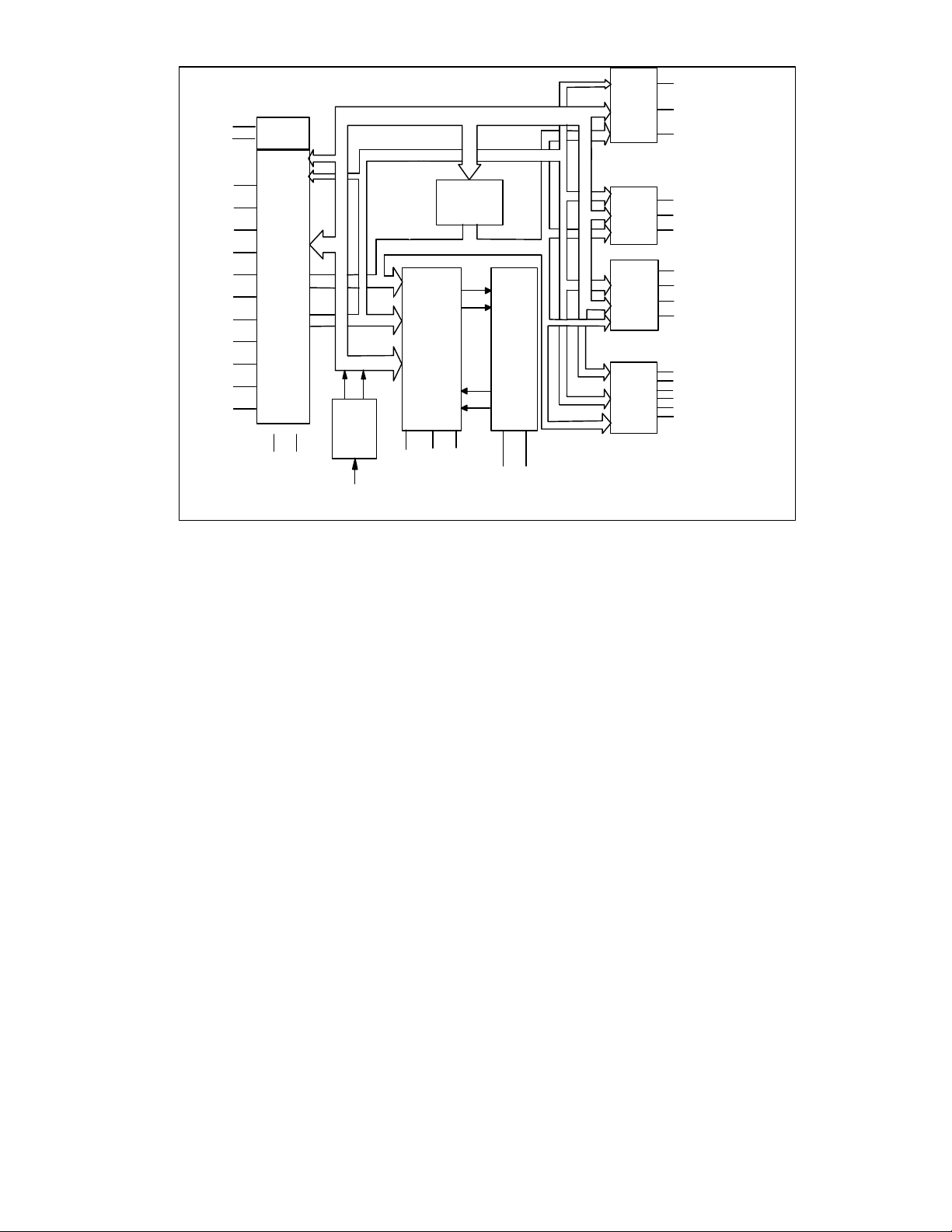
SER_IRQ
*
Denotes Multifunction Pins
PCI_CLK
SERIAL
IRQ
ADDRESS BUS
DATA BUS
MULTI-MODE
PARALLEL
PORT/FDC
MUX
PD0-7
BUSY, SLCT, PE,
nERROR, nACK
nSTB, nSLCTIN,
nINIT, nALF
nIOR
nIOW
AEN
SA[0:11] (nCS)*
SA[12-15]*
SD[O:7]
DRQ[1:3]
nDACK[1:3]*
RESET_DRV
IOCHRDY
CONFIGURATION
REGISTERS
16C550
COMPATIBLE
SERIAL
PORT 1
TXD1, nCTS1, nRTS1
RXD1
nDSR1, nDCD1, nRI1, nDTR1
CONTROL BUS
HOST
CPU
INTERFACE
PROPRIETARY
COMPATIBLE
FLOPPYDISK
TC
CONTROLLER
SMSC
82077
VERTICAL
CORE
WDATA
WCLOCK
RCLOCK
DIGITAL
DATA
SEPARATOR
WITH WRITE
PRECOM-
PENSATION
RDATA
16C550
COMPATIBLE
SERIAL
PORT 2 WITH
INFRARED
8042
CLOCK
*
IRRX, IRTX
TXD2(IRTX), nCTS2, nRTS2
RXD2(IRRX)
nDSR2, nDCD2, nRI2, nDTR2
KCLK
KDATA
MCLK
MDATA
GATEA20, KRESET
*
P12, P16
*
*
* * *
*
*
*
*
GEN
Vcc Vss
ICLOCK
(14.318)
nINDEX
nTRK0
nDSKCHG
nWRPRT
nWGATE
nDIR
nSTEP
nHDSEL
nDS0,1
nMTR0,1
DRVDEN0
DRVDEN1
nWDATA nRDATA
*
DENSEL
FIGURE 1 - FDC37M60x BLOCK DIAGRAM

11
FUNCTIONAL DESCRIPTION
SUPER I/O REGISTERS
The address map, shown below in Table 1,
shows the addresses of the different blocks of
the Super I/O immediately after power up. The
base addresses of the FDC, serial and parallel
ports can be moved via the configuration
registers. Some addresses are used to access
more than one register.
Table 1 - Super I/O Block Addresses
ADDRESS BLOCK NAME
Base+(0-5) and +(7) Floppy Disk 0
Base+(0-7) Serial Port Com 1 4
Base1+(0-7)
Base+(0-3)
Base+(0-7)
Base+(0-3), +(400-402)
Base+(0-7), +(400-402)
60, 64 KYBD 7
Note 1: Refer to the configuration register descriptions for setting the base address
Serial Port Com 2 5 IR Support
Parallel Port
SPP
EPP
ECP
ECP+EPP+SPP
HOST PROCESSOR INTERFACE
The host processor communicates with the
FDC37M60x through a series of read/write
registers. The port addresses for these registers
are shown in Table 1. Register access is
accomplished through programmed I/O or DMA
transfers. All registers are 8 bits wide. All host
interface output buffers are capable of sinking a
minimum of 24 mA.
LOGICAL
DEVICE NOTES
3

12
FLOPPY DISK CONTROLLER
FDC INTERNAL REGISTERS
The Floppy Disk Controller (FDC) provides the
interface between a host microprocessor and
the floppy disk drives. The FDC integrates the
functions of the Formatter/Controller, Digital
Data Separator, Write Precompensation and
Data Rate Selection logic for an IBM XT/AT
compatible FDC. The true CMOS 765B core
guarantees 100% IBM PC XT/AT compatibility
in addition to providing data overflow and
underflow protection.
The FDC is compatible to the 82077AA using
SMSC's proprietary floppy disk controller core.
Table 2 - Status, Data and Control Registers
(Shown with base addresses of 3F0 and 370)
PRIMARY
ADDRESS
3F0
3F1
3F2
3F3
3F4
3F4
3F5
3F6
3F7
3F7
SECONDARY
ADDRESS R/W REGISTER
370
371
372
373
374
374
375
376
377
377
The Floppy Disk Controller contains eight
internal registers which facilitate the interfacing
between the host microprocessor and the disk
drive. Table 2 shows the addresses required to
access these registers. Registers other than the
ones shown are not supported. The rest of the
description assumes that the primary addresses
have been selected.
R
Status Register A (SRA)
R
Status Register B (SRB)
R/W
R/W
W
R/W
W
Digital Output Register (DOR)
Tape Drive Register (TSR)
R
Main Status Register (MSR)
Data Rate Select Register (DSR)
Data (FIFO)
Reserved
R
Digital Input Register (DIR)
Configuration Control Register (CCR)

13
STATUS REGISTER A (SRA)
Address 3F0 READ ONLY
This register is read-only and monitors the state
of the FINTR pin and several disk
PS/2 Mode
7 6 5 4 3 2 1 0
INT
nDRV2 STEP nTRK0 HDSEL nINDX nWP DIR
PENDING
RESET
0 N/A 0 N/A 0 N/A N/A 0
COND.
interface pins in PS/2 and Model 30 modes. The
SRA can be accessed at any time when in PS/2
mode. In the PC/AT mode the data bus pins D0
- D7 are held in a high impedance state for a
read of address 3F0.
BIT 0 DIRECTION
Active high status indicating the direction of
head movement. A logic "1" indicates inward
direction; a logic "0" indicates outward direction.
BIT 1 nWRITE PROTECT
Active low status of the WRITE PROTECT disk
interface input. A logic "0" indicates that the disk
is write protected.
BIT 2 nINDEX
Active low status of the INDEX disk interface
input.
BIT 3 HEAD SELECT
Active high status of the HDSEL disk interface
input. A logic "1" selects side 1 and a logic "0"
selects side 0.
BIT 4 nTRACK 0
Active low status of the TRK0 disk interface
input.
BIT 5 STEP
Active high status of the STEP output disk
interface output pin.
BIT 6 nDRV2
Active low status of the DRV2 disk interface
input pin, indicating that a second drive has
been installed.
BIT 7 INTERRUPT PENDING
Active high bit indicating the state of the Floppy
Disk Interrupt output.

14
PS/2 Model 30 Mode
RESET
COND.
7 6 5 4 3 2 1 0
INT
PENDING
0 0 0 N/A 1 N/A N/A 1
DRQ STEP
F/F
TRK0 nHDSEL INDX WP nDIR
BIT 0 nDIRECTION
Active low status indicating the direction of head
movement. A logic "0" indicates inward
direction; a logic "1" indicates outward direction.
BIT 1 WRITE PROTECT
Active high status of the WRITE PROTECT disk
interface input. A logic "1" indicates that the disk
is write protected.
BIT 2 INDEX
Active high status of the INDEX disk interface
input.
BIT 3 nHEAD SELECT
Active low status of the HDSEL disk interface
input. A logic "0" selects side 1 and a logic "1"
selects side 0.
BIT 4 TRACK 0
Active high status of the TRK0 disk interface
input.
BIT 5 STEP
Active high status of the latched STEP disk
interface output pin. This bit is latched with the
STEP output going active, and is cleared with a
read from the DIR register, or with a hardware
or software reset.
BIT 6 DMA REQUEST
Active high status of the DRQ output pin.
BIT 7 INTERRUPT PENDING
Active high bit indicating the state of the Floppy
Disk Interrupt output.

15
STATUS REGISTER B (SRB)
Address 3F1 READ ONLY
This register is read-only and monitors the state
of several disk interface pins in PS/2 and
PS/2 Mode
7 6 5 4 3 2 1 0
RESET
1 1 DRIVE
SEL0
1 1 0 0 0 0 0 0
WDATA
TOGGLE
COND.
Model 30 modes. The SRB can be accessed at
any time when in PS/2 mode. In the PC/AT
mode the data bus pins D0 - D7 are held in a
high impedance state for a read of address 3F1.
RDATA
TOGGLE
WGATE MOT
EN1
MOT
EN0
BIT 0 MOTOR ENABLE 0
Active high status of the MTR0 disk interface
output pin. This bit is low after a hardware reset
and unaffected by a software reset.
BIT 1 MOTOR ENABLE 1
Active high status of the MTR1 disk interface
output pin. This bit is low after a hardware reset
and unaffected by a software reset.
BIT 2 WRITE GATE
Active high status of the WGATE disk interface
output.
BIT 3 READ DATA TOGGLE
Every inactive edge of the RDATA input causes
this bit to change state.
BIT 4 WRITE DATA TOGGLE
Every inactive edge of the WDATA input causes
this bit to change state.
BIT 5 DRIVE SELECT 0
Reflects the status of the Drive Select 0 bit of
the DOR (address 3F2 bit 0). This bit is cleared
after a hardware reset and it is unaffected by a
software reset.
BIT 6 RESERVED
Always read as a logic "1".
BIT 7 RESERVED
Always read as a logic "1".

16
PS/2 Model 30 Mode
nDRV2 nDS1 nDS0 WDATA
RESET
COND.
7 6 5 4 3 2 1 0
F/F
RDATA
F/F
WGATE
F/F
nDS3 nDS2
N/A 1 1 0 0 0 1 1
BIT 0 nDRIVE SELECT 2
Active low status of the DS2 disk interface
output.
BIT 1 nDRIVE SELECT 3
Active low status of the DS3 disk interface
output.
BIT 2 WRITE GATE
Active high status of the latched WGATE output
signal. This bit is latched by the active going
edge of WGATE and is cleared by the read of
the DIR register.
BIT 3 READ DATA
Active high status of the latched RDATA output
signal. This bit is latched by the inactive going
edge of RDATA and is cleared by the read of the
DIR register.
BIT 4 WRITE DATA
Active high status of the latched WDATA output
signal. This bit is latched by the inactive going
edge of WDATA and is cleared by the read of
the DIR register. This bit is not gated with
WGATE.
BIT 5 nDRIVE SELECT 0
Active low status of the DS0 disk interface
output.
BIT 6 nDRIVE SELECT 1
Active low status of the DS1 disk interface
output.
BIT 7 nDRV2
Active low status of the DRV2 disk interface
input.

17
DIGITAL OUTPUT REGISTER (DOR)
Address 3F2 READ/WRITE
The DOR controls the drive select and motor
enables of the disk interface outputs. It
7 6 5 4 3 2 1 0
MOT
EN3
RESET
MOT
EN2
MOT
EN1
0 0 0 0 0 0 0 0
COND.
also contains the enable for the DMA logic and a
software reset bit. The contents of the DOR are
unaffected by a software reset. The DOR can
be written to at any time.
MOT
EN0
DMAEN nRESETDRIVE
SEL1
DRIVE
SEL0
BIT 0 and 1 DRIVE SELECT
These two bits are binary encoded for the four
drive selects DS0 -DS3, thereby allowing only
one drive to be selected at one time.
BIT 2 nRESET
A logic "0" written to this bit resets the Floppy
disk controller. This reset will remain active
until a logic "1" is written to this bit. This
software reset does not affect the DSR and CCR
registers, nor does it affect the other bits of the
DOR register. The minimum reset duration
required is 100ns, therefore toggling this bit by
consecutive writes to this register is a valid
method of issuing a software reset.
BIT 3 DMAEN
PC/AT and Model 30 Mode:
Writing this bit to logic "1" will enable the DRQ,
nDACK, TC and FINTR outputs. This bit being
a logic "0" will disable the nDACK and TC
inputs, and hold the DRQ and FINTR outputs in
a high impedance state. This bit is a logic "0"
after a reset and in these modes.
PS/2 Mode: In this mode the DRQ, nDACK, TC
and FINTR pins are always enabled. During a
reset, the DRQ, nDACK, TC, and FINTR pins
will remain enabled, but this bit will be cleared to
a logic "0".
BIT 4 MOTOR ENABLE 0
This bit controls the MTR0 disk interface output.
A logic "1" in this bit will cause the output pin to
go active.
BIT 5 MOTOR ENABLE 1
This bit controls the MTR1 disk interface output.
A logic "1" in this bit will cause the output pin to
go active.
BIT 6 MOTOR ENABLE 2
This bit controls the MTR2 disk interface output.
A logic "1" in this bit will cause the output pin to
go active.
BIT 7 MOTOR ENABLE 3
This bit controls the MTR3 disk interface output.
A logic "1" in this bit causes the output to go
active.
Table 3 - Drive Activation Values
DRIVE DOR VALUE
0
1
2
3
1CH
2DH
4EH
8FH

18
TAPE DRIVE REGISTER (TDR)
Address 3F3 READ/WRITE
The Tape Drive Register (TDR) is included for
82077 software compatibility and allows the
user to assign tape support to a particular drive
during initialization. Any future references to
that drive automatically invokes tape support.
The TDR Tape Select bits TDR [1:0] determine
the tape drive number. Table 4 illustrates the
TAPE SEL1
Table 4- Tape Select Bits
TAPE SEL0
(TDR.1)
(TDR.0)
0
0
1
1
DRIVE
SELECTED
0
None
1
0
1
Tape Select bit encoding. Note that drive “0” is
the boot device and cannot be assigned tape
support. The remaining Tape Drive Register
bits TDR.[7:2] are tristated when read. The TDR
is unaffected by a software reset.
Table 5 - Internal 2 Drive Decode - Normal
DIGITAL OUTPUT REGISTER
DRIVE SELECT
OUTPUTS (ACTIVE LOW)
MOTOR ON OUTPUTS
(ACTIVE LOW)
Bit 7 Bit 6 Bit 5 Bit 4 Bit1 Bit 0 nDS1 nDS0 nMTR1 nMTR0
X X X 1 0 0 1 0 nBIT 5 nBIT 4
X X 1 X 0 1 0 1 nBIT 5 nBIT 4
X 1 X X 1 0 1 1 nBIT 5 nBIT 4
1 X X X 1 1 1 1 nBIT 5 nBIT 4
0 0 0 0 X X 1 1 nBIT 5 nBIT 4
1
2
3
Table 6 - Internal 2 Drive Decode - Drives 0 and 1 Swapped
DIGITAL OUTPUT REGISTER
DRIVE SELECT
OUTPUTS (ACTIVE
MOTOR ON OUTPUTS
(ACTIVE LOW)
LOW)
Bit 7 Bit 6 Bit 5 Bit 4 Bit1 Bit 0 nDS1 nDS0 nMTR1 nMTR0
X X X 1 0 0 0 1 nBIT 4 nBIT 5
X X 1 X 0 1 1 0 nBIT 4 nBIT 5
X 1 X X 1 0 1 1 nBIT 4 nBIT 5
1 X X X 1 1 1 1 nBIT 4 nBIT 5
0 0 0 0 X X 1 1 nBIT 4 nBIT 5

19
Normal Floppy Mode
Normal mode. Register 3F3 contains only bits 0 and 1. When this register is read, bits 2-7 are a
high impedance.
DB7 DB6 DB5 DB4 DB3 DB2 DB1 DB0
REG 3F3 Tri-state Tri-state Tri-state Tri-state Tri-state Tri-state tape sel1 tape sel0
Enhanced Floppy Mode 2 (OS2)
Register 3F3 for Enhanced Floppy Mode 2 operation.
DB7 DB6 DB5 DB4 DB3 DB2 DB1 DB0
REG 3F3 Media
ID1
Media
ID0
Drive Type ID Floppy Boot Drive tape sel1 tape sel0
For this mode, MEDIA_ID[1:0] pins are gated
into bits 6 and 7 of the 3F3 register. These two
bits are not affected by a hard or soft reset.
BIT 7 MEDIA ID 1 READ ONLY (Pin 19) (See
Table 7)
BIT 6 MEDIA ID 0 READ ONLY (Pin 20) (See
Table 8)
BITS 5 and 4 Drive Type ID - These bits reflect
two of the bits of L0-CRF1. Which two bits
these are depends on the last drive selected in
the Digital Output Register (3F2). (See Table 9)
Table 7 - Media ID1
Input MEDIA ID1
BIT 7
Pin 19 L0-CRF1-B5
= 0
L0-CRF1-B5
= 1
0 0 1
1 1 0
Note: L0-CRF1-B5 = Logical Device 0,
Configuration Register F1, Bit 5
BITS 3 and 2 Floppy Boot Drive - These bits
reflect the value of L0-CRF1. Bit 3 = L0-CRF1B7. Bit 2 = L0-CRF1-B6.
Bits 1 and 0 - Tape Drive Select
(READ/WRITE). Same as in Normal and
Enhanced Floppy Mode 1.
Table 8 - Media ID0
Input MEDIA ID0
BIT 6
Pin 20 CRF1-B4
= 0
CRF1-B4
= 1
0 0 1
1 1 0

20
Table 9 - Drive Type ID
DIGITAL OUTPUT REGISTER REGISTER 3F3 - DRIVE TYPE ID
Bit 1 Bit 0 Bit 5 Bit 4
0 0 L0-CRF2 - B1 L0-CRF2 - B0
0 1 L0-CRF2 - B3 L0-CRF2 - B2
1 0 L0-CRF2 - B5 L0-CRF2 - B4
1 1 L0-CRF2 - B7 L0-CRF2 - B6
Note: L0-CRF2-Bx = Logical Device 0, Configuration Register F2, Bit x.

21
DATA RATE SELECT REGISTER (DSR)
Address 3F4 WRITE ONLY
This register is write only. It is used to program
the data rate, amount of write precompensation,
power down status, and software reset. The
data rate is programmed using the
Configuration Control Register (CCR) not the
DSR, for PC/AT and PS/2 Model
7 6 5 4 3 2 1 0
S/W
RESET
RESET
POWER
0 PRE-
DOWN
0 0 0 0 0 0 1 0
COND.
BIT 0 and 1 DATA RATE SELECT
These bits control the data rate of the floppy
controller. See Table 11 for the settings
corresponding to the individual data rates. The
data rate select bits are unaffected by a
software reset, and are set to 250 Kbps after a
hardware reset.
BIT 2 through 4 PRECOMPENSATION
SELECT
These three bits select the value of write
precompensation that will be applied to the
WDATA output signal. Table 10 shows the
precompensation values for the combination of
these bits settings. Track 0 is the default
starting track number to start precompensation.
this starting track number can be changed by
the configure command.
BIT 5 UNDEFINED
Should be written as a logic "0".
BIT 6 LOW POWER
A logic "1" written to this bit will put the floppy
controller into manual low power mode. The
floppy controller clock and data Note: The
DSR is Shadowed in the Floppy Data Rate
Select Shadow Register, LD8:CRC2[7:0],
30 and Microchannel applications. Other
applications can set the data rate in the DSR.
The data rate of the floppy controller is the most
recent write of either the DSR or CCR. The DSR
is unaffected by a software reset. A hardware
reset will set the DSR to 02H, which
corresponds to the default precompensation
setting and 250 Kbps.
COMP2
PRE-
COMP1
PRE-
COMP0
DRATE
SEL1
DRATE
separator circuits will be turned off. The
controller will come out of manual low power
mode after a software reset or access to the
Data Register or Main Status Register.
BIT 7 SOFTWARE RESET
This active high bit has the same function as the
DOR RESET (DOR bit 2) except that this bit is
self clearing.
Table 10 - Precompensation Delays
PRECOMP
432
111
001
010
011
100
101
110
000
PRECOMPENSATION DELAY
(nsec)
<2Mbps 2Mbps*
0.00
41.67
83.34
125.00
166.67
208.33
250.00
Default
Default: See Table 12
*2Mbps data rate is only available if Vcc= 5V.
SEL0
0
20.8
41.7
62.5
83.3
104.2
125
Default

22
Table 11 - Data Rates
DRIVE RATE DATA RATE DATA RATE
DRT1 DRT0 SEL1 SEL0 MFM FM 1 0
0 0 1 1 1Meg --- 1 1 1
0 0 0 0 500 250 1 0 0
0 0 0 1 300 150 0 0 1
0 0 1 0 250 125 0 1 0
0 1 1 1 1Meg --- 1 1 1
0 1 0 0 500 250 1 0 0
0 1 0 1 500 250 0 0 1
0 1 1 0 250 125 0 1 0
1 0 1 1 1Meg --- 1 1 1
1 0 0 0 500 250 1 0 0
1 0 0 1 2Meg --- 0 0 1
1 0 1 0 250 125 0 1 0
Drive Rate Table (Recommended) 00 = 360K, 1.2M, 720K, 1.44M and 2.88M Vertical Format
01 = 3-Mode Drive
10 = 2 Meg Tape
Note 1: The DRATE and DENSEL values are mapped onto the DRVDEN pins.
DENSEL
DRATE(1)
Table 12 - DRVDEN Mapping
DT1 DT0 DRVDEN1 (1) DRVDEN0 (1) DRIVE TYPE
0 0 DRATE0 DENSEL 4/2/1 MB 3.5"
2/1 MB 5.25" FDDS
2/1.6/1 MB 3.5" (3-
MODE)
1 0 DRATE0 DRATE1
0 1 DRATE0 nDENSEL PS/2
1 1 DRATE1 DRATE0

23
Table 13 - Default Precompensation Delays
PRECOMPENSATION
DATA RATE
2 Mbps*
1 Mbps
500 Kbps
300 Kbps
250 Kbps
*The 2Mbps data rate is only available if VCC = 5V.
DELAYS
20.8 ns
41.67 ns
125 ns
125 ns
125 ns

24
MAIN STATUS REGISTER
Address 3F4 READ ONLY
The Main Status Register is a read-only register
and indicates the status of the disk controller.
The Main Status Register can be read at any
7 6 5 4 3 2 1 0
RQM DIO NON
DMA
CMD
BUSY
time. The MSR indicates when the disk
controller is ready to receive data via the Data
Register. It should be read before each byte
transferring to or from the data register except in
DMA mode. No delay is required when reading
the MSR after a data transfer.
DRV3
BUSY
DRV2
BUSY
DRV1
BUSY
DRV0
BUSY
BIT 0 - 3 DRV x BUSY
These bits are set to 1s when a drive is in the
seek portion of a command, including implied
and overlapped seeks and recalibrates.
BIT 4 COMMAND BUSY
This bit is set to a “1” when a command is in
progress. This bit will go active after the
command byte has been accepted and goes
inactive at the end of the results phase. If there
is no result phase (Seek, Recalibrate
commands), this bit is returned to a “0” after the
last command byte.
BIT 5 NON-DMA
This mode is selected in the SPECIFY
command and will be set to a “1” during the
execution phase of a command. This is for
polled data transfers and helps differentiate
between the data transfer phase and the reading
of result bytes.
BIT 6 DIO
Indicates the direction of a data transfer once a
RQM is set. A “1” indicates a read and a “0”
indicates a write is required.
BIT 7 RQM
Indicates that the host can transfer data if set to
a “1”. No access is permitted if set to a “0”.

25
DATA REGISTER (FIFO)
Address 3F5 READ/WRITE
All command parameter information, disk data
and result status are transferred between the
host processor and the floppy disk controller
through the Data Register.
Data transfers are governed by the RQM and
DIO bits in the Main Status Register.
The Data Register defaults to FIFO disabled
mode after any form of reset. This maintains
PC/AT hardware compatibility. The default
values can be changed through the Configure
command (enable full FIFO operation with
threshold control). The advantage of the FIFO
is that it allows the system a larger DMA
latency without causing a disk error. Table 14
gives several examples of the delays with a
Table 14 - FIFO Service Delay
FIFO THRESHOLD
EXAMPLES
1 byte
2 bytes
8 bytes
15 bytes
MAXIMUM DELAY TO SERVICING AT 2
1 x 4 µs - 1.5 µs = 2.5 µs
2 x 4 µs - 1.5 µs = 6.5 µs
8 x 4 µs - 1.5 µs = 30.5 µs
15 x 4 µs - 1.5 µs = 58.5 µs
FIFO. The data is based upon the following
formula:
Threshold # x 1
DATA RATE
x 8
- 1.5 µs = DELAY
At the start of a command, the FIFO action is
always disabled and command parameters
must be sent based upon the RQM and DIO bit
settings. As the command execution phase is
entered, the FIFO is cleared of any data to
ensure that invalid data is not transferred.
An overrun or underrun will terminate the
current command and the transfer of data. Disk
writes will complete the current sector by
generating a 00 pattern and valid CRC. Reads
require the host to remove the remaining data
so that the result phase may be entered.
Mbps* DATA RATE
FIFO THRESHOLD
EXAMPLES
1 byte
2 bytes
8 bytes
15 bytes
FIFO THRESHOLD
EXAMPLES
1 byte
2 bytes
8 bytes
15 bytes
MAXIMUM DELAY TO SERVICING AT 1
Mbps DATA RATE
1 x 8 µs - 1.5 µs = 6.5 µs
2 x 8 µs - 1.5 µs = 14.5 µs
8 x 8 µs - 1.5 µs = 62.5 µs
15 x 8 µs - 1.5 µs = 118.5 µs
MAXIMUM DELAY TO SERVICING AT
500 Kbps DATA RATE
1 x 16 µs - 1.5 µs = 14.5 µs
2 x 16 µs - 1.5 µs = 30.5 µs
8 x 16 µs - 1.5 µs = 126.5 µs
15 x 16 µs - 1.5 µs = 238.5 µs
*The 2 Mbps data rate is only available if VCC = 5V.

26
DIGITAL INPUT REGISTER (DIR)
Address 3F7 READ ONLY
This register is read-only in all modes.
PC-AT Mode
7 6 5 4 3 2 1 0
DSK
CHG
RESET
N/A N/A N/A N/A N/A N/A N/A N/A
COND.
BIT 0 - 6 UNDEFINED
The data bus outputs D0 - 6 will remain in a
high impedance state during a read of this
register.
PS/2 Mode
7 6 5 4 3 2 1 0
DSK
1 1 1 1 DRATE
CHG
RESET
N/A N/A N/A N/A N/A N/A N/A 1
COND.
BIT 0 nHIGH DENS
This bit is low whenever the 500 Kbps or 1
Mbps data rates are selected, and high when
250 Kbps and 300 Kbps are selected.
BITS 1 - 2 DATA RATE SELECT
These bits control the data rate of the floppy
controller. See Table 11 for the settings
corresponding to the individual data rates. The
data rate select bits are unaffected by a
software reset, and are set to 250 Kbps after a
hardware reset.
BIT 7 DSKCHG
This bit monitors the pin of the same name and
reflects the opposite value seen on the disk
cable or the value programmed in the Force
Disk Change Register (see Configuration
Register LD8:CRC1[1:0]).
SEL1
DRATE
SEL0
nHIGH
nDENS
BITS 3 - 6 UNDEFINED
Always read as a logic "1"
BIT 7 DSKCHG
This bit monitors the pin of the same name
and reflects the opposite value seen on the
disk cable or the value programmed in the
Force Disk Change Register (see
Configuration Register LD8:CRC1[1:0]).

27
Model 30 Mode
RESET
COND.
7 6 5 4 3 2 1 0
DSK
CHG
N/A 0 0 0 0 0 1 0
0 0 0 DMAEN NOPREC DRATE
SEL1
DRATE
SEL0
BITS 0 - 1 DATA RATE SELECT
These bits control the data rate of the floppy
controller. See Table 11 for the settings
corresponding to the individual data rates. The
data rate select bits are unaffected by a
software reset, and are set to 250 Kbps after a
hardware reset.
BIT 2 NOPREC
This bit reflects the value of NOPREC bit set in
the CCR register.
BIT 3 DMAEN
This bit reflects the value of DMAEN bit set in
the DOR register bit 3.
BITS 4 - 6 UNDEFINED
Always read as a logic "0"
BIT 7 DSKCHG
This bit monitors the pin of the same name and
reflects the opposite value seen on the disk
cable or the value programmed in the Force
Disk Change Register (see Configuration
Register LD8:CRC1[1:0]).

28
CONFIGURATION CONTROL REGISTER (CCR)
Address 3F7 WRITE ONLY
PC/AT and PS/2 Modes
7 6 5 4 3 2 1 0
RESET
N/A N/A N/A N/A N/A N/A 1 0
COND.
DRATE
SEL1
DRATE
SEL0
BIT 0 and 1 DATA RATE SELECT 0 and 1
These bits determine the data rate of the floppy
controller. See Table 11 for the appropriate
values.
PS/2 Model 30 Mode
7 6 5 4 3 2 1 0
RESET
N/A N/A N/A N/A N/A N/A 1 0
COND.
BIT 0 and 1 DATA RATE SELECT 0 and 1
These bits determine the data rate of the floppy
controller. See Table 11 for the appropriate
values.
BIT 2 NO PRECOMPENSATION
This bit can be set by software, but it has no
functionality. It can be read by bit 2 of the DSR
when in Model 30 register mode. Unaffected by
software reset.
BIT 2 - 7 RESERVED
Should be set to a logical "0"
NOPREC DRATE
SEL1
DRATE
SEL0
BIT 3 - 7 RESERVED
Should be set to a logical "0"
Table 12 shows the state of the DENSEL pin.
The DENSEL pin is set high after a hardware
reset and is unaffected by the DOR and the
DSR resets.

29
STATUS REGISTER ENCODING
During the Result Phase of certain commands, the Data Register contains data bytes that give
the status of the command just executed.
Table 15 - Status Register 0
BIT NO. SYMBOL NAME DESCRIPTION
7,6 IC Interrupt
Code
5 SE Seek End The FDC completed a Seek, Relative Seek or
4 EC Equipment
Check
3 Unused. This bit is always "0".
2 H Head
Address
1,0 DS1,0 Drive Select The current selected drive.
00 - Normal termination of command. The specified
command was properly executed and completed
without error.
01 - Abnormal termination of command. Command
execution was started, but was not successfully
completed.
10 - Invalid command. The requested command
could not be executed.
11 - Abnormal termination caused by Polling.
Recalibrate command (used during a Sense Interrupt
Command).
The TRK0 pin failed to become a "1" after:
1. 80 step pulses in the Recalibrate command.
2. The Relative Seek command caused the FDC to
step outward beyond Track 0.
The current head address.

30
Table 16 - Status Register 1
BIT NO. SYMBOL NAME DESCRIPTION
7 EN End of
Cylinder
6 Unused. This bit is always "0".
5 DE Data Error The FDC detected a CRC error in either the ID field or
4 OR Overrun/
Underrun
3 Unused. This bit is always "0".
2 ND No Data Any one of the following:
1 NW Not Writable WP pin became a "1" while the FDC is executing a
0 MA Missing
Address Mark
The FDC tried to access a sector beyond the final
sector of the track (255D). Will be set if TC is not
issued after Read or Write Data command.
the data field of a sector.
Becomes set if the FDC does not receive CPU or DMA
service within the required time interval, resulting in
data overrun or underrun.
1. Read Data, Read Deleted Data command - the
FDC did not find the specified sector.
2. Read ID command - the FDC cannot read the ID
field without an error.
3. Read A Track command - the FDC cannot find the
proper sector sequence.
Write Data, Write Deleted Data, or Format A Track
command.
Any one of the following:
1. The FDC did not detect an ID address mark at the
specified track after encountering the index pulse
from the IDX pin twice.
2. The FDC cannot detect a data address mark or a
deleted data address mark on the specified track.
 Loading...