

Standard Microsystems Corporation FDC37C669FR Datasheet

FDC37C669FR
Super I/O Floppy Disk Controller with Fast Infrared
Support
FEATURES
• 5 Volt Operation
• Intelligent Auto Power Management
• 16 Bit Address Qualification (Optional)
• 2.88MB Super I/O Floppy Disk Controller
- Licensed CMOS 765B Floppy Disk
Controller
- Software and Register Compatible with
SMSC's Proprietary 82077AA
Compatible Core
- Supports Two Floppy Drives Directly
- Supports Vertical Recording Format
- 16 Byte Data FIFO
- 100% IBM® Compatibility
- Detects All Overrun and Underrun
Conditions
- Sophisticated Power Control Circuitry
(PCC) Including Multiple Powerdown
Modes for Reduced Power Consumption
- DMA Enable Logic
- Data Rate and Drive Control Registers
- Swap Drives A and B
- Non-Burst Mode DMA Option
- 48 Base I/O Address, Seven IRQ and
Three DMA Options
• Floppy Disk Available on Parallel Port Pins
• Enhanced Digital Data Separator
- 2 Mbps, 1 Mbps, 500 Kbps, 300 Kbps,
250 Kbps Data Rates
- Programmable Precompensation Modes
• Serial Ports
- Two High Speed NS16C550 Compatible
UARTs with Send/Receive 16 Byte FIFOs
- Supports 230k and 460k Baud
- Programmable Baud Rate Generator
- Modem Control Circuitry
- Infrared - IrDA, HPSIR, ASKIR, Fast IR
(4Mbps IrDA), Consumer IR Support
- Alternate IR Pins (Optional)
- 96 Base I/O Address and Seven IRQ
Options
• Multi-Mode Parallel Port with ChiProtect
- Standard Mode
- IBM PC/XT®, PC/AT®, and PS/2
Compatible Bidirectional Parallel Port
- Enhanced Parallel Port (EPP)
Compatible
- EPP 1.7 and EPP 1.9 (IEEE 1284 Compliant)
- Enhanced Capabilities Port (ECP)
Compatible (IEEE 1284 Compliant)
- Incorporates ChiProtect Circuitry for
Protection Against Damage Due to
Printer Power-On
- 192 Base I/O Address, Seven IRQ and
Three DMA Options
• ISA Host Interface
• IDE Interface (Optional)
- On-Chip Decode and Select Logic
Compatible with IBM PC/XT and PC/AT
Embedded Hard Disk Drives
- 48 Base I/O Address and Seven IRQ
Options
• Game Port Select Logic
- 48 Base I/O Addresses
• General Purpose Address Decoder
- 16 Byte Block Decode
- 48 Base I/O Address Options
• 100 Pin QFP and TQFP Package

2
TABLE OF CONTENTS
FEATURES...................................................................................................................................1
GENERAL DESCRIPTION.............................................................................................................3
QFP PIN CONFIGURATION.......................................................................................................... 4
TQFP PIN CONFIGURATION........................................................................................................5
DESCRIPTION OF PIN FUNCTIONS ............................................................................................ 6
FUNCTIONAL DESCRIPTION.......................................................................................................18
SUPER I/O REGISTERS.......................................................................................................... 18
HOST PROCESSOR INTERFACE...........................................................................................18
FLOPPY DISK CONTROLLER ...................................................................................................... 19
FLOPPY DISK CONTROLLER INTERNAL REGISTERS..........................................................19
COMMAND SET/DESCRIPTIONS............................................................................................41
INSTRUCTION SET.................................................................................................................45
PARALLEL PORT FLOPPY DISK CONTROLLER..........................................................................73
SERIAL PORT (UART)..................................................................................................................75
INFRARED INTERFACE................................................................................................................90
FAST IR........................................................................................................................................91
PARALLEL PORT..........................................................................................................................93
IBM XT/AT COMPATIBLE, BI-DIRECTIONAL AND EPP MODES.............................................94
EXTENDED CAPABILITIES PARALLEL PORT.........................................................................101
AUTO POWER MANAGEMENT....................................................................................................114
INTEGRATED DRIVE ELECTRONICS INTERFACE...................................................................... 120
CONFIGURATION.........................................................................................................................121
OPERATIONAL DESCRIPTION.....................................................................................................143
MAXIMUM GUARANTEED RATINGS.......................................................................................143
DC ELECTRICAL CHARACTERISTICS.................................................................................... 143
TIMING DIAGRAMS......................................................................................................................147
ECP PARALLEL PORT TIMING...............................................................................................164
80 Arkay Drive
Hauppauge, NY 11788
(516) 435-6000
FAX (516) 273-3123

3
GENERAL DESCRIPTION
The SMSC FDC37C669FR PC 95/96
Compatible Super I/O Floppy Disk Controller
with Infrared Support utilizes SMSC's proven
SuperCell technology for increased product
reliability and functionality. The FDC37C669FR
is PC95/96 compliant and is optimized for
motherboard applications. The FDC37C669FR
supports both 1 Mbps and 2 Mbps data rates
and vertical recording operation at 1 Mbps Data
Rate.
The FDC37C669FR incorporates SMSC's true
CMOS 765B floppy disk controller, advanced
digital data separator, 16 byte data FIFO, two
16C550 compatible UARTs, one Multi-Mode
parallel port which includes ChiProtect circuitry
plus EPP and ECP support, IDE interface, onchip 12 mA AT bus drivers, game port chip
select and two floppy direct drive support. The
true CMOS 765B core provides 100%
compatibility with IBM PC/XT and PC/AT
architectures in addition to providing data
overflow and underflow protection. The SMSC
advanced digital data separator incorporates
SMSC's patented data separator technology,
allowing for ease of testing and use. Both onchip UARTs are compatible with the NS16C550.
One UART includes additional support for a
Serial Infrared Interface, complying with IrDA,
HPSIR, and ASKIR formats (used by Sharp,
Apple Newton, and other PDAs) as well as Fast
IR and Consumer IR. The parallel port, the IDE
interface, and the game port select logic are
compatible with IBM PC/AT architectures. The
FDC37C669FR incorporates sophisticated
power control circuitry (PCC). The PCC
supports multiple low power down modes.
The FDC37C669FR Floppy Disk Controller
incorporates Software Configurable Logic (SCL)
for ease of use. Use of the SCL feature allows
programmable system configuration of key
functions such as the FDC, parallel port, and
UARTs. The parallel port ChiProtect prevents
damage caused by the printer being powered
when the FDC37C669FR is not powered.
The FDC37C669FR does not require any
external filter components, and is, therefore
easy to use and offers lower system cost and
reduced board area. The FDC37C669FR is
software and register compatible with SMSC's
proprietary 82077AA core.
IBM, PC/XT and PC/AT are registered trademarks and PS/2 is
a trademark of International Business Machines Corporation.
SMSC is a registered trademark and ChiProtect, SuperCell,
and Multi-Mode are trademarks of Standard Microsystems
Corporation

4
PIN CONFIGURATION
D2
D1
D0
VSS
AEN
nIOW
nIOR
A9
A8
A7
IRQ_F
IRQ_E
IRQ_D
IRQ_C
nDACK_B
TC
A6
A5
A4
A3
50
49
48
47
46
45
44
43
42
41
40
39
38
37
36
35
34
33
32
31
81
82
83
84
85
86
87
88
89
90
91
92
93
94
95
96
97
98
99
100
FDC37C669FR
100 Pin QFP
nRTS1
nCTS1
nDTR1
nRI1
nDCD1
nRI2
nDCD2
RXD2/IRRX
TXD2/IRTX
nDSR2
nRTS2
nCTS2
nDTR2
DRV2/ADRX/IRQ_B
VSS
nDACK_C
A10
NC
DRQ_C
IOCHRDY
DRVDEN0
nMTR0
nDS1
nDS0
nMTR1
VSS
nDIR
nSTEP
nWDATA
nWGATE
nHDSEL
nINDEX
nTRK0
nWRTPRT
VCC
nRDATA
nDSKCHG
DRVDEN1
IRQ_A
CLK14
DRQ_A
nDACK_A
IR Mode/IRR3/IRQIN
nIDEEN/IRQ_H
nHDCS0/IRRX2
nHDCS1/IRTX2
A11/nCS
A0A1A2
nDSR1
TXD1
RXD1
nSTROBE
nAUTOFD
nERROR
nINIT
nSLCTIN
VCC
PD0
PD1
PD2
PD3
VSS
PD4
PD5
PD6
PD7
nACK
BUSYPESLCT
PWRGD/GAMECS
RESETD7D6D5D4
DRQ_B
D3
21 3 4 5 6 7 8 9 10 11 12 13 14 15 16 17 18 19 20 21 22 23 24 25 26 27 28 29 30
7980 78 77 76 75 74 73 72 71 70 69 68 67 66 65 64 63 62 61 60 59 58 57 56 55 54 53 52 51

5
FDC37C669FR
100 Pin TQFP
nSTROBE
nAUTOFD
nERROR
nINIT
nSLCTIN
VCC
PD0
PD1
PD2
PD3
VSS
PD4
PD5
PD6
PD7
nACK
BUSYPESLCT
PWRGD/GAMECS
RESETD7D6D5D4
75 74 73 72 71 70 69 68 67 66 65 64 63 62 61 60 59 58 57 56 55 54 53 52 51
nRTS1
nCTS1
nDTR1
nRI1
nDCD1
nRI2
nDCD2
RXD2/IRRX
TXD2/IRTX
nDSR2
nRTS2
nCTS2
nDTR2
DRV2/ADRX/IRQ_B
VSS
nDACK_C
A10
NC
DRQ_C
IOCHRDY
DRVDEN0
nMTR0
nDSR1
TXD1
RXD1
81
82
83
84
85
86
87
88
89
90
91
92
93
94
95
96
97
98
99
100
80
79
78
76
77
50
49
48
47
46
45
44
43
42
41
40
39
38
37
36
35
34
33
32
31
30
29
28
27
26
D2
D1
D0
VSS
AEN
nIOW
nIOR
A9
A8
A7
IRQ_F
IRQ_E
IRQ_D
IRQ_C
nDACK_B
TC
A6
A5
A4
A3
A0
A1
A2
DRQ_B
D3
nDS1
nDS0
nMTR1
VSS
nDIR
nSTEP
nWDATA
nWGATE
nHDSEL
nINDEX
nTRK0
nWRTPRT
VCC
nRDATA
nDSKCHG
DRVDEN1
IRQ_A
CLK14
DRQ_A
nDACK_A
IR Mode/IRR3/IRQIN
nIDEEN/IRQ_H
nHDCS0/IRRX2
nHDCS1/IRTX2
A11/nCS
21 3 4 5 6 7 8 9 10 11 12 13 14 15 16 17 18 19 20 21 22 23 24 25

6
DESCRIPTION OF PIN FUNCTIONS
QFP
PIN
NO. NAME SYMBOL
BUFFER
TYPE DESCRIPTION
HOST PROCESSOR INTERFACE
48-51
53-56
Data Bus 0-7 D0-D7 I/O24 The data bus connection used by the
host microprocessor to transmit data to
and from the chip. These pins are in a
high-impedance state when not in the
output mode.
44 nI/O Read nIOR I This active low signal is issued by the
host microprocessor to indicate a read
operation.
45 nI/O Write nIOW I This active low signal is issued by the
host microprocessor to indicate a write
operation.
46 Address
Enable
AEN I Active high Address Enable indicates
DMA operations on the host data bus.
Used internally to qualify appropriate
address decodes.
28-34
41-43,
97
I/O Address A0-A10 I These host address bits determine the
I/O address to be accessed during nIOR
and nIOW cycles. These bits are latched
internally by the leading edge of nIOR
and nIOW. All internal address decodes
use the full A0 to A10 address bits.
21,52,99DMA Request
A, B, C
DRQ_A
DRQ_B
DRQ_C
O24 This active high output is the DMA
request for byte transfers of data
between the host and the chip. This
signal is cleared on the last byte of the
data transfer by the nDACK signal going
low (or by nIOR going low if nDACK was
already low as in demand mode).
22,36,96nDMA
Acknowledge
A, B, C
nDACK_A
nDACK_B
nDACK_C
I An active low input acknowledging the
request for a DMA transfer of data
between the host and the chip. This
input enables the DMA read or write
internally.

7
DESCRIPTION OF PIN FUNCTIONS
QFP
PIN
NO. NAME SYMBOL
BUFFER
TYPE DESCRIPTION
35 Terminal
Count
TC I This signal indicates to the chip that
DMA data transfer is complete. TC is
only accepted when nDACK_x is low. In
AT and PS/2 Model 30 modes, TC is
active high and in PS/2 mode, TC is
active low.
19,
37-40,
Interrupt
Request
A, C, D,
E, F
IRQ_A
IRQ_C
IRQ_D
IRQ_E
IRQ_F
O24
OD24
The interrupt request from the logical
device or IRQIN is output on one of the
IRQA-G signals. Refer to the
configuration registers for more
information.
If EPP or ECP Mode is enabled, this
output is pulsed low, then released to
allow sharing of interrupts.
27 Chip Select
Input
nCS I When enabled, this active low pin serves
as an input for an external decoder
circuit which is used to qualify address
lines above A10.
57 Reset RESET IS This active high signal resets the chip
and must be valid for 500ns minimum.
The effect on the internal registers is
described in the appropriate section.
The configuration registers are not
affected by this reset.
FLOPPY DISK INTERFACE
16 nRead Disk
Data
nRDATA IS Raw serial bit stream from the disk drive,
low active. Each falling edge represents
a flux transition of the encoded data.
10 nWrite
Gate
nWGATE OD48 This active low high current driver allows
current to flow through the write head. It
becomes active just prior to writing to the
diskette.
9 nWrite
Data
nWDATA OD48 This active low high current driver
provides the encoded data to the disk
drive. Each falling edge causes a flux
transition on the media.

8
DESCRIPTION OF PIN FUNCTIONS
QFP
PIN
NO. NAME SYMBOL
BUFFER
TYPE DESCRIPTION
11 nHead
Select
nHDSEL OD48 This high current output selects the
floppy disk side for reading or writing. A
logic "1" on this pin means side 0 will be
accessed, while a logic "0" means side 1
will be accessed.
7 Direction
Control
nDIR OD48 This high current low active output
determines the direction of the head
movement. A logic "1" on this pin means
outward motion, while a logic "0" means
inward motion.
8 nStep Pulse nSTEP OD48 This active low high current driver issues
a low pulse for each track-to-track
movement of the head.
17 Disk Change nDSKCHG IS This input senses that the drive door is
open or that the diskette has possibly
been changed since the last drive
selection. This input is inverted and read
via bit 7 of I/O address 3F7H.
4,3 nDrive Select
O,1
nDS0,1 OD48 These active low open drain outputs
select drives 0-1.
2,5 nMotor On 0,1 nMTR0,1 OD48 These active low open drain outputs
select motor drives 0-1.
1 DRVDEN0 DRVDEN0 OD48 Indicates the drive and media selected.
Refer to configuration registers CR03,
CR0B, CR1F.
14 nWrite
Protected
nWRTPRT IS This active low Schmitt Trigger input
senses from the disk drive that a disk is
write protected. Any write command is
ignored.
13 wTrack 00 nTRK00 IS This active low Schmitt Trigger input
senses from the disk drive that the head
is positioned over the outermost track.
12 nIndex nINDEX IS This active low Schmitt Trigger input
senses from the disk drive that the head
is positioned over the beginning of a
track, as marked by an index hole.

9
DESCRIPTION OF PIN FUNCTIONS
QFP
PIN
NO. NAME SYMBOL
BUFFER
TYPE DESCRIPTION
18 DRVDEN1 DRVDEN 1 OD48 Indicates the drive and media selected.
Refer to configuration registers CR03,
CR0B, CR1F.
SERIAL PORT INTERFACE
88
Receive
Data 2
RXD2/IRRX I Receiver serial data input for port 2. IR
Receive Data
89 Transmit
Data 2
TXD2/IRTX O24 Transmit serial data output for port 2. IR
transmit data.
78 Receive
Data 1
RXD1 I Reciever serial data input for port 1.
79 Transmit
Data 1
TXD1 024 Transmit serial data output for port 1.
81,91 nRequest to
Send
(System
Option)
nRTS1
nRTS2
(SYSOPT)
O4 Active low Request to Send outputs for
the Serial Port. Handshake output signal
notifies modem that the UART is ready
to transmit data. This signal can be
programmed by writing to bit 1 of
Modem Control Register (MCR). The
hardware reset will reset the nRTS signal
to inactive mode (high). Forced inactive
during loop mode operation.
At the trailing edge of hardware reset,
the nRTS2 input is latched to determine
the configuration base address:
0 : INDEX Base I/O Address = 3F0 Hex
1 : INDEX Base I/O Address = 370 Hex
83,93 nData
Terminal
Ready
nDTR1
nDTR2
O4 Active low Data Terminal Ready outputs
for the serial port. Handshake output
signal notifies modem that the UART is
ready to establish data communication
link. This signal can be programmed by
writing to bit 0 of Modem Control
Register (MCR). The hardware reset will
reset the nDTR signal to inactive mode
(high). Forced inactive during loop mode
operation.

10
DESCRIPTION OF PIN FUNCTIONS
QFP
PIN
NO. NAME SYMBOL
BUFFER
TYPE DESCRIPTION
82,92 nClear to
Send
nCTS1
nCTS2
I Active low Clear to Send inputs for the
serial port. Handshake signal which
notifies the UART that the modem is
ready to receive data. The CPU can
monitor the status of nCTS signal by
reading bit 4 of Modem Status Register
(MSR). A nCTS signal state change
from low to high after the last MSR read
will set MSR bit 0 to a 1. If bit 3 of
Interrupt Enable Register is set, the
interrupt is generated when nCTS
changes state. The nCTS signal has no
effect on the transmitter. Note: Bit 4 of
MSR is the complement of nCTS.
80,90 nData Set
Ready
nDSR1
nDSR2
I Active low Data Set Ready inputs for the
serial port. Handshake signal which
notifies the UART that the modem is
ready to establish the communication
link. The CPU can monitor the status of
nDSR signal by reading bit 5 of Modem
Status Register (MSR). A nDSR signal
state change from low to high after the
last MSR read will set MSR bit 1 to a 1.
If bit 3 of Interrupt Enable Register is set,
the interrupt is generated when nDSR
changes state. Note: Bit 5 of MSR is
the complement of nDSR.
85,87 nData Carrier
Detect
nDCD1
nDCD2
I Active low Data Carrier Detect inputs for
the serial port. Handshake signal which
notifies the UART that carrier signal is
detected by the modem. The CPU can
monitor the status of nDCD signal by
reading bit 7 of Modem Status Register
(MSR). A nDCD signal state change
from low to high after the last MSR read
will set MSR bit 3 to a 1. If bit 3 of
Interrupt Enable Register is set, the
interrupt is generated when nDCD
changes state. Note: Bit 7 of MSR is
the complement of nDCD.

11
DESCRIPTION OF PIN FUNCTIONS
QFP
PIN
NO. NAME SYMBOL
BUFFER
TYPE DESCRIPTION
84,86 nRing
Indicator
nRI1
nRI2
I Active low Ring Indicator inputs for the
serial port. Handshake signal which
notifies the UART that the telephone ring
signal is detected by the modem. The
CPU can monitor the status of nRI signal
by reading bit 6 of Modem Status
Register (MSR). A nRI signal state
change from low to high after the last
MSR read will set MSR bit 2 to a 1. If bit
3 of Interrupt Enable Register is set, the
interrupt is generated when nRI changes
state. Note: Bit 6 of MSR is the
complement of nRI.
PARALLEL PORT INTERFACE
73 nPrinter Select
Input
nSLCTIN OD24
0P24
This active low output selects the printer.
This is the complement of bit 3 of the
Printer Control Register.
Refer to Parallel Port description for use
of this pin in ECP and EPP mode.
74 nInitiate
Output
nINIT OD24
0P24
This output is bit 2 of the printer control
register. This is used to initiate the
printer when low.
Refer to Parallel Port description for use
of this pin in ECP and EPP mode.
76 nAutofeed
Output
nAUTOFD OD24
0P24
This output goes low to cause the printer
to automatically feed one line after each
line is printed. The nAUTOFD output is
the complement of bit 1 of the Printer
Control Register.
Refer to Parallel Port description for use
of this pin in ECP and EPP mode.

12
DESCRIPTION OF PIN FUNCTIONS
QFP
PIN
NO. NAME SYMBOL
BUFFER
TYPE DESCRIPTION
77 nStrobe
Output
nSTROBE OD24
0P24
An active low pulse on this output is
used to strobe the printer data into the
printer. The nSTROBE output is the
complement of bit 0 of the Printer
Control Register.
Refer to Parallel Port description for use
of this pin in ECP and EPP mode.
61 Busy BUSY I This is a status output from the printer, a
high indicating that the printer is not
ready to receive new data. Bit 7 of the
Printer Status Register is the
complement of the BUSY input. Refer to
Parallel Port description for use of this
pin in ECP and EPP mode.
62
nAcknowledge
nACK I A low active output from the printer
indicating that it has received the data
and is ready to accept new data. Bit 6 of
the Printer Status Register reads the
nACK input. Refer to Parallel Port
description for use of this pin in ECP and
EPP mode.
60 Paper End PE I Another status output from the printer, a
high indicating that the printer is out of
paper. Bit 5 of the Printer Status
Register reads the PE input. Refer to
Parallel Port description for use of this
pin in ECP and EPP mode.
59 Printer
Selected
Status
SLCT I This high active output from the printer
indicates that it has power on. Bit 4 of
the Printer Status Register reads the
SLCT input. Refer to Parallel Port
description for use of this pin in ECP and
EPP mode.
75 nError nERROR I A low on this input from the printer
indicates that there is a error condition at
the printer. Bit 3 of the Printer Status
register reads the nERR input. Refer to
Parallel Port description for use of this
pin in ECP and EPP mode.
13
DESCRIPTION OF PIN FUNCTIONS
QFP
PIN
NO. NAME SYMBOL
BUFFER
TYPE DESCRIPTION
63-66
68-71
Port Data PD0-PD7 I/O24 The bi-directional parallel data bus is
used to transfer information between
CPU and peripherals.
100 IOCHRDY IOCHRDY OD24P In EPP mode, this pin is pulled low to
extend the read/write command. This pin
has an internal pull-up.
IDE/ALT IR PINS
24 nIDE Enable
Interrupt
Request H
nIDEEN
IRQ_H
O24P
(Note 1)
024
OD24
This active low signal is active when the
IDE is enabled and the I/O address is
accessing an IDE register.
The interrupt request from a logical
device or IRQIN may be output on the
IRQH signal. Refer to the configuration
registers for more information.
If EPP or ECP Mode is enabled, this
output is pulsed low, then released to
allow sharing of interrupts.
25 nIDE Chip
Select 0
IRRX2
nHDCS0
IRRX2
O24P
(Note 1)
I
This is the Hard Disk Chip select
corresponding to the eight control block
addresses.
Alternate IR Receive input
26 nIDE Chip
Select 1
IR Transmit 2
nHDCS1
IRTX2
O24P
(Note 1)
O24P
This is the Hard Disk Chip select
corresponding to the alternate status
register.
Alternate IR transmit output
MISCELLANEOUS
20 CLOCK 14 CLK14 ICLK The external connection to a single
source 14.318 MHz clock.

14
DESCRIPTION OF PIN FUNCTIONS
QFP
PIN
NO. NAME SYMBOL
BUFFER
TYPE DESCRIPTION
94 Drive 2
Address X
Interrupt
Request B
DRV2
nADRX
IRQ_B
I
OD24
024
(OD24)
In PS/2 mode, this input indicates
whether a second drive is connected;
DRV2 should be low if a second drive is
connected. This status is reflected in a
read of Status Register A.
Active low address decode out, used to
decode a 1, 8, or 16 byte address block.
(An external pull-up is required). Refer to
Configuration registers CR03, CR08 and
CR09 for more information. This pin has
a 30 ua internal pull-up.
The interrupt request from a logical
device or IRQIN may be output on
IRQ_B. Refer to the configuration
registers for more information.
(If EPP or ECP Mode is enabled, this
output is pulsed low, then released to
allow sharing of interrupts.)
23 IRQIN
IRMode/
IRR3
I/O8
I/O8
This pin is used to steer an interrupt
signal from an external device onto one
of eight IRQ outputs IRQA-H.
IR Mode pin or second IR receive pin for
Fast IR.

15
DESCRIPTION OF PIN FUNCTIONS
QFP
PIN
NO. NAME SYMBOL
BUFFER
TYPE DESCRIPTION
58 PWRGD
nGAMECS
I
O4
This active high input indicates that the
power (VCC) is valid. For device
operation, PWRGD must be active.
When PWRGD is inactive, all inputs to
the device are disconnected and put into
a low power mode; all outputs are put
into high impedance. The contents of all
registers are preserved as long as V
CC
has a valid value. The driver current
drain in this mode drops to ISTBY standby current. This input has an
internal 30 ua pull-up.
This is the Game Port Chip Select output
- active low. It will go active when the I/O
address, qualified by AEN, matches that
selected in Configuration register CR1E.
98 No Connect NC No Connect
15,72 Power V
CC
Positive Supply Voltage.
6,47,
67,95
Ground GND Ground Supply.
Note 1: Refer to Configuration Register 00 for information on the pull-ups for these pins.
Note: IDE does not decode for 377, 3F7
Note: RI and the Serial interrupt is always active if system power is applied to the chip.

16
BUFFER TYPE DESCRIPTIONS
BUFFER TYPE
DESCRIPTION
I/O8
I/O24
Input/Output. 8mA sink; 4mA source
Input/Output. 24mA sink; 12mA source
O24 Output. 24mA sink; 12mA source
OD48 Open drain. 48mA sink
O4 Output. 4mA sink; 2mA source
OD24 Output. 24mA sink
OD24P
Open drain. 24mA sink; 30µA source
O24P Output. 24mA sink; 12mA source with 30µA pull-up
OCLK Output to external crystal
ICLK Input to Crystal Oscillator Circuit (CMOS levels)
I Input TTL compatible.
IS Input with Schmitt Trigger.
17
FIGURE 1 - FDC37C669FR BLOCK DIAGRAM
nDSR1, nDCD1, nRI, nDTR1
TXD1, nCTS1, nRTS1
nINIT, nAUTOFD
HOST
CPU
MULTI-MODE
PARALLEL
PORT/FDC
MUX
16C550
COMPATIBLE
SERIAL
PORT 1
16C550
COMPATIBLE
SERIAL
PORT 2 WITH
INFRARED
IDE
CONFIGURATION
REGISTERS
POWER
MANAGEMENT
INTERFACE
INTERFACE
CONTROL BUS
ADDRESS BUS
DATA BUS
CLOCK
GEN
nINDEX
nTRK0
nDSKCHG
nWRPRT
nWGATE
nDIR
nSTEP
DRVDEN0
DRVDEN1
DRV2(nADRX)(IRQB)
nDS0,1,2
nMTR0,1,2
RDATA
RCLOCK
WDATA
WCLOCK
nWDATA nRDATA
nHDCSO(IRRX2)
RXD1
PD0-7
BUSY, SLCT, PE,
nERROR, nACK
nSTROBE, nSLCTIN,
5 V
Vcc (2)
Vss (4)
SMSC
PROPRIETARY
82077 COMPATIBLE
VERTICAL
FLOPPYDISK
CONTROLLER
CORE
DIGITAL
DATA
SEPARATOR
WITH WRITE
PRECOM-
PENSATION
GENERAL
PURPOSE
ADDRESS
DECODER
ADRX
TXD2(IRTX),nCTS2,nRTS2
nGAMECS
nHDCS1(IRTX2)
nIDEEN(IRQH)
nCS
nIOR
nIOW
AEN
A0-A10
D0-D7
DRQ_A-C
nDACK_A-C
TC
IRQ_C-F
IRQIN
IOCHRDY
RESET
RXD2(IRRX)
GAME
PORT
DECODER
IRQA
nDSR2,nDCD2,nRI2,nDTR2
14.318
CLOCK
PWRGD
IR Mode, IRR3*
*Multifunction Pin

18
FUNCTIONAL DESCRIPTION
SUPER I/O REGISTERS
The address map, shown below in Table 1,
shows the addresses of the different blocks of
the Super I/O immediately after power up. The
base addresses of the FDC, IDE, serial and
parallel ports can be moved via the
configuration registers. Some addresses are
used to access more than one register.
HOST PROCESSOR INTERFACE
The host processor communicates with the
FDC37C669FR through a series of read/write
registers. The port addresses for these registers
are shown in Table 1. Register access is
accomplished through programmed I/O or DMA
transfers. All registers are 8 bits wide except
the IDE data register at port 1F0H which is 16
bits wide. All host interface output buffers are
capable of sinking a minimum of 12 mA.
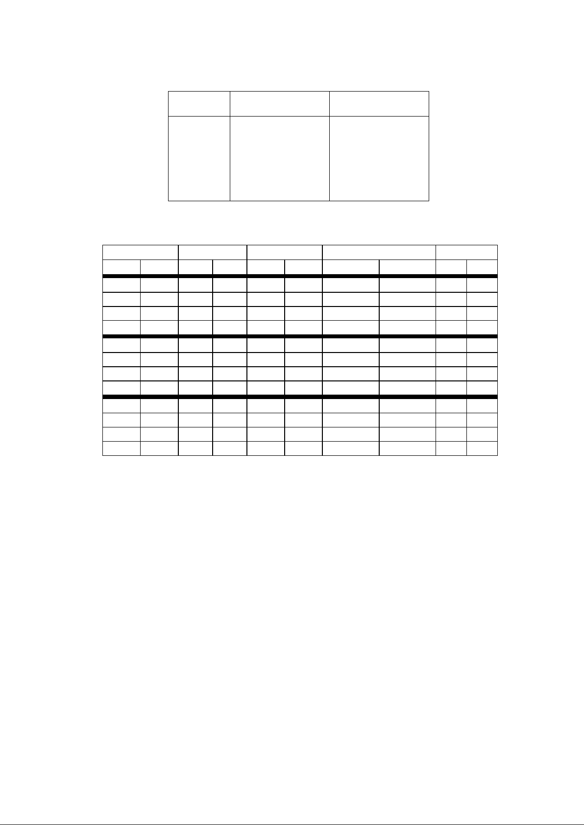
Table 1 - FDC37C669FR Block Addresses
ADDRESS BLOCK NAME NOTES
3F0, 3F1 or 370, 371 Configuration Write only; Note 1, 2
Base +0,1 Floppy Disk Read only; Disabled at power
up; Note 2
Base +[2:5, 7] Floppy Disk Disabled at power up; Note 2
Base +[0:7] Serial Port Com 1 Disabled at power up; Note 2
Base1 +[0:7]
Base2 +[0:7]
Serial Port Com 2
Disabled at power up; Note 2
Base +[0:3] all modes
Base +[4:7] for EPP
Base +[400:403] for ECP
Parallel Port Disabled at power up; Note 2
Base1 +[0:7]
Base2 +[6]
IDE Disabled at power up; Note 2
Note 1: Configuration registers can only be modified in configuration mode, refer to the configuration
register description for more information. Access to status registers A and B of the floppy
disk is disabled in configuration mode.
Note 2: The base addresses must be set in the configuration registers before accessing the logical
devices.

19
FLOPPY DISK CONTROLLER
The Floppy Disk Controller (FDC) provides the
interface between a host microprocessor and
the floppy disk drives. The FDC integrates the
functions of the Formatter/Controller, Digital
Data Separator, Write Precompensation and
Data Rate Selection logic for an IBM XT/AT
compatible FDC. The true CMOS 765B core
guarantees 100% IBM PC XT/AT compatibility
in addition to providing data overflow and
underflow protection.
The FDC37C669FR is compatible to the
82077AA using SMSC's proprietary floppy disk
controller core.
FLOPPY DISK CONTROLLER INTERNAL
REGISTERS
The Floppy Disk Controller contains eight
internal registers which facilitate the interfacing
between the host microprocessor and the disk
drive. Table 2 shows the addresses required to
access these registers. Registers other than the
ones shown are not supported. The rest of the
FDC description assumes the Base I/O Address
is 3F0.
Table 2 - Status, Data and Control Registers
BASE I/O
ADDRESS REGISTER
+0
+1
+2
+3
+4
+4
+5
+6
+7
+7
R
R
R/W
R/W
R
W
R/W
R
W
Status Register A
Status Register B
Digital Output Register
Tape Drive Register
Main Status Register
Data Rate Select Register
Data (FIFO)
Reserved
Digital Input Register
Configuration Control Register
SRA
SRB
DOR
TSR
MSR
DSR
FIFO
DIR
CCR
For information on the floppy disk on Parallel Port pins, refer to Configuration Register CR4 and
Parallel Port Floppy Disk Controller description.

20
STATUS REGISTER A (SRA)
Address 3F0 READ ONLY
This register is read-only and monitors the state
of the FINTR pin and several disk
interface pins, in PS/2 and Model 30 modes.
The SRA can be accessed at any time when in
PS/2 mode. In the PC/AT mode the data bus
pins D0-D7 are held in a high impedance state
for a read of address 3F0.
PS/2 Mode
BIT 0 DIRECTION
Active high status indicating the direction of
head movement. A logic "1" indicates inward
direction; a logic "0" indicates outward direction.
BIT 1 nWRITE PROTECT
Active low status of the WRITE PROTECT disk
interface input. A logic "0" indicates that the disk
is write protected.
BIT 2 nINDEX
Active low status of the INDEX disk interface
input.
BIT 3 HEAD SELECT
Active high status of the HDSEL disk interface
input. A logic "1" selects side 1 and a logic "0"
selects side 0.
BIT 4 nTRACK 0
Active low status of the TRK0 disk interface
input.
BIT 5 STEP
Active high status of the STEP output disk
interface output pin.
BIT 6 nDRV2
Active low status of the DRV2 disk interface
input pin, indicating that a second drive has
been installed.
BIT 7 INTERRUPT PENDING
Active high bit indicating the state of the Floppy
Disk Interrupt output.
7 6 5 4 3 2 1 0
INT
PENDING
nDRV2 STEP nTRK0 HDSEL nINDX nWP DIR
RESET
COND.
0 N/A 0 N/A 0 N/A N/A 0

21
PS/2 Model 30 Mode
BIT 0 nDIRECTION
Active low status indicating the direction of head
movement. A logic "0" indicates inward
direction, a logic "1" indicates outward direction.
BIT 1 WRITE PROTECT
Active high status of the WRITE PROTECT disk
interface input. A logic "1" indicates that the disk
is write protected.
BIT 2 INDEX
Active high status of the INDEX disk interface
input.
BIT 3 nHEAD SELECT
Active low status of the HDSEL disk interface
input. A logic "0" selects side 1 and a logic "1"
selects side 0.
BIT 4 TRACK 0
Active high status of the TRK0 disk interface
input.
BIT 5 STEP
Active high status of the latched STEP disk
interface output pin. This bit is latched with the
STEP output going active, and is cleared with a
read from the DIR register, or with a hardware
or software reset.
BIT 6 DMA REQUEST
Active high status of the DRQ output pin.
BIT 7 INTERRUPT PENDING
Active high bit indicating the state of the Floppy
Disk Interrupt output.
STATUS REGISTER B (SRB)
Address F1 READ ONLY
This register is read-only and monitors the state
of several disk interface pins, in PS/2 and Model
30 modes. The SRB can be accessed at any
time when in PS/2 mode. In the PC/AT mode
the data bus pins D0 - D7 are held in a high
impedance state for a read of address 3F1.
7 6 5 4 3 2 1 0
INT
PENDING
DRQ STEP
F/F
TRK0 nHDSEL INDX WP nDIR
RESET
COND.
0 0 0 N/A 1 N/A N/A 1

22
PS/2 Mode
BIT 0 MOTOR ENABLE 0
Active high status of the MTR0 disk interface
output pin. This bit is low after a hardware reset
and it is unaffected by a software reset.
BIT 1 MOTOR ENABLE 1
Active high status of the MTR1 disk interface
output pin. This bit is low after a hardware reset
and it is unaffected by a software reset.
BIT 2 WRITE GATE
Active high status of the WGATE disk interface
output.
BIT 3 READ DATA TOGGLE
Every inactive edge of the RDATA input causes
this bit to change state.
BIT 4 WRITE DATA TOGGLE
Every inactive edge of the WDATA input causes
this bit to change state.
BIT 5 DRIVE SELECT 0
Reflects the status of the Drive Select 0 bit of
the DOR (address 3F2 bit 0). This bit is cleared
after a hardware reset and it is unaffected by a
software reset.
BIT 6 RESERVED
Always read as a logic "1".
BIT 7 RESERVED
Always read as a logic "1".
7 6 5 4 3 2 1 0
1 1 DRIVE
SEL0
WDATA
TOGGLE
RDATA
TOGGLE
WGATE MOT
EN1
MOT
EN0
RESET
COND.
1 1 0 0 0 0 0 0

23
PS/2 Model 30 Mode
BIT 0 nDRIVE SELECT 2
Active low status of the DS2 disk interface
output.
BIT 1 nDRIVE SELECT 3
Active low status of the DS3 disk interface
output.
BIT 2 WRITE GATE
Active high status of the latched WGATE output
signal. This bit is latched by the active going
edge of WGATE and is cleared by the read of
the DIR register.
BIT 3 READ DATA
Active high status of the latched RDATA output
signal. This bit is latched by the inactive going
edge of RDATA and is cleared by the read of the
DIR register.
BIT 4 WRITE DATA
Active high status of the latched WDATA output
signal. This bit is latched by the inactive going
edge of WDATA and is cleared by the read of
the DIR register. This bit is not gated with
WGATE.
BIT 5 nDRIVE SELECT 0
Active low status of the DS0 disk interface
output.
BIT 6 nDRIVE SELECT 1
Active low status of the DS1 disk interface
output.
BIT 7 nDRV2
Active low status of the DRV2 disk interface
input.
7 6 5 4 3 2 1 0
nDRV2 nDS1 nDS0 WDATA
F/F
RDATA
F/F
WGATE
F/F
nDS3 nDS2
RESET
COND.
N/A 1 1 0 0 0 1 1

24
DIGITAL OUTPUT REGISTER (DOR)
Address 3F2 READ/WRITE
The DOR controls the drive select and motor
enables of the disk interface outputs. It
also contains the enable for the DMA logic
and contains a software reset bit. The contents
of the DOR are unaffected by a software reset.
The DOR can be written to at any time.
BIT 0 and 1 DRIVE SELECT
These two bit a are binary encoded for the four
drive selects DS0-DS3, thereby allowing only
one drive to be selected at one time.
BIT 2 nRESET
A logic "0" written to this bit resets the Floppy
disk controller. This reset will remain active
until a logic "1" is written to this bit. This
software reset does not affect the DSR and CCR
registers, nor does it affect the other bits of the
DOR register. The minimum reset duration
required is 100ns, therefore toggling this bit by
consecutive writes to this register is a valid
method of issuing a software reset.
BIT 3 DMAEN
PC/AT and Model 30 Mode:
Writing this bit to logic "1" will enable the DRQ,
nDACK, TC and FINTR outputs. This bit being
a logic "0" will disable the nDACK and TC
inputs, and hold the DRQ and FINTR outputs in
a high impedance state. This bit is a logic "0"
after a reset and in these modes.
PS/2 Mode: In this mode the DRQ, nDACK, TC
and FINTR pins are always enabled. During a
reset, the DRQ, nDACK, TC, and FINTR pins
will remain enabled, but this bit will be cleared to
a logic "0".
BIT 4 MOTOR ENABLE 0
This bit controls the MTR0 disk interface output.
A logic "1" in this bit will cause the output pin to
go active.
BIT 5 MOTOR ENABLE 1
This bit controls the MTR1 disk interface output.
A logic "1" in this bit will cause the output pin to
go active.
BIT 6 MOTOR ENABLE 2
This bit controls the MTR2 disk interface output.
A logic "1" in this bit will cause the output pin to
go active.
BIT 7 MOTOR ENABLE 3
This bit controls the MTR3 disk interface output.
A logic "1" in this bit causes the output to go
active.
7 6 5 4 3 2 1 0
MOT
EN3
MOT
EN2
MOT
EN1
MOT
EN0
DMAEN nRESET DRIVE
SEL1
DRIVE
SEL0
RESET
COND.
0 0 0 0 0 0 0 0
25
Table 3 - Drive Activation Values
DRIVE DOR VALUE
0 1CH
1 2DH
2 4EH
3 8FH
TAPE DRIVE REGISTER (TDR)
Address 3F3 READ/WRITE
This register is included for 82077 software
compatability. The robust digital data
separator used in the FDC37C669FR does not
require its characteristics modified for tape
support. The contents of this register are not
used internal to the device. The TDR is
unaffected by a software reset. Bits 2-7 are tristated when read in this mode.
Table 4- Tape Select Bits
Table 5 - Internal 4 Drive Decode - Normal
DIGITAL OUTPUT REGISTER
DRIVE SELECT OUTPUTS
(ACTIVE LOW)
MOTOR ON OUTPUTS
(ACTIVE LOW)
Bit 7 Bit 6 Bit 5 Bit 4 Bit1 Bit 0 nDS3 nDS2 nDS1 nDS0 nMTR3 nMTR2 nMTR1 nMTR0
X X X 1 0 0 1 1 1 0 nBIT 7 nBIT 6 nBIT 5 nBIT 4
X X 1 X 0 1 1 1 0 1 nBIT 7 nBIT 6 nBIT 5 nBIT 4
X 1 X X 1 0 1 0 1 1 nBIT 7 nBIT 6 nBIT 5 nBIT 4
1 X X X 1 1 0 1 1 1 nBIT 7 nBIT 6 nBIT 5 nBIT 4
0 0 0 0 X X 1 1 1 1 nBIT 7 nBIT 6 nBIT 5 nBIT 4
Table 6 - Internal 4 Drive Decode - Drives 0 and 1 Swapped
DIGITAL OUTPUT REGISTER
DRIVE SELECT OUTPUTS
(ACTIVE LOW)
MOTOR ON OUTPUTS
(ACTIVE LOW)
Bit 7 Bit 6 Bit 5 Bit 4 Bit1 Bit 0 nDS3 nDS2 nDS1 nDS0 nMTR3 nMTR2 nMTR1 nMTR0
X X X 1 0 0 1 1 0 1 nBIT 7 nBIT 6 nBIT 4 nBIT 5
X X 1 X 0 1 1 1 1 0 nBIT 7 nBIT 6 nBIT 4 nBIT 5
X 1 X X 1 0 1 0 1 1 nBIT 7 nBIT 6 nBIT 4 nBIT 5
1 X X X 1 1 0 1 1 1 nBIT 7 nBIT 6 nBIT 4 nBIT 5
0 0 0 0 X X 1 1 1 1 nBIT 7 nBIT 6 nBIT 4 nBIT 5
TAPE SEL1 TAPE SEL2
DRIVE
SELECTED
0
0
1
1
0
1
0
1
None
1
2
3
26
Table 7 - External 2 to 4 Drive Decode - Normal
DIGITAL OUTPUT REGISTER DRIVE SELECT
OUTPUTS
(ACTIVE LOW)
MOTOR ON OUTPUTS
(ACTIVE LOW)
Bit 7 Bit 6 Bit 5 Bit 4 Bit1 Bit 0 nDS1 nDS0 nMTR1 nMTR0
X X X 1 0 0 0 0 1 0
X X 1 X 0 1 0 1 1 0
X 1 X X 1 0 1 0 1 0
1 X X X 1 1 1 1 1 0
X X X 0 0 0 0 0 1 1
X X 0 X 0 1 0 1 1 1
X 0 X X 1 0 1 0 1 1
0 X X X 1 1 1 1 1 1
Table 8 - External 2 to 4 Drive Decode - Drives 0 and 1 Swapped
DIGITAL OUTPUT REGISTER DRIVE SELECT
OUTPUTS
(ACTIVE LOW)
MOTOR ON OUTPUTS
(ACTIVE LOW)
Bit 7 Bit 6 Bit 5 Bit 4 Bit1 Bit 0 nDS1 nDS0 nMTR1 nMTR0
X X X 1 0 0 0 1 1 0
X X 1 X 0 1 0 0 1 0
X 1 X X 1 0 1 0 1 0
1 X X X 1 1 1 1 1 0
X X X 0 0 0 0 1 1 1
X X 0 X 0 1 0 0 1 1
X 0 X X 1 0 1 0 1 1
0 X X X 1 1 1 1 1 1

27
Normal Floppy Mode
Normal mode. Register 3F3 contains only
bits 0 and 1. When this register is read, bits 2 7 are a high impedance.
DB7 DB6 DB5 DB4 DB3 DB2 DB1 DB0
REG 3F3 Tri-state Tri-state Tri-state Tri-state Tri-state Tri-state tape sel1 tape sel0
Enhanced Floppy Mode 2 (OS2)
Register 3F3 for Enhanced Floppy Mode 2 operation.
DB7 DB6 DB5 DB4 DB3 DB2 DB1 DB0
REG 3F3 Reserved Reserved Drive Type ID Floppy Boot Drive tape sel1 tape sel0
For this mode, DRATE0 and DRATE1 pins are
inputs, and these inputs are gated into bits 6
and 7 of the 3F3 register. These two bits are
not affected by a hard or soft reset.
BIT 7 and 6 RESERVED
BIT 5 and 4 DRIVE TYPE ID - These Bits
reflect two of the bits of configuration
register 6.
Which two bits depends on the last drive
selected in the Digital Output Register (3F2).
(See Table 11)
BIT 3 and 2 FLOPPY BOOT DRIVE - These
bits reflect the value of configuration register 7
bits 1, 0. Bit 3 = CR7 Bit DB1. Bit 2 = CR7 Bit
DB0.
BIT 1 and 0 - Tape Drive Select
(READ/WRITE). Same as in Normal and
Enhanced Floppy Mode. 1.
Table 9 - Drive Type ID
DIGITAL OUTPUT REGISTER REGISTER 3F3 - DRIVE TYPE ID
Bit 1 Bit 0 Bit 5 Bit 4
0 0 CR6 - Bit 1 CR6 - Bit 0
0 1 CR6 - Bit 3 CR6 - Bit 2
1 0 CR6 - Bit 5 CR6 - Bit 4
1 1 CR6 - Bit 7 CR6 - Bit 6

28
DATA RATE SELECT REGISTER (DSR)
Address 3F4 WRITE ONLY
This register is write only. It is used to program
the data rate, amount of write precompensation,
power down status, and software reset. The
data rate is programmed using the
Configuration Control Register (CCR),
not the DSR, for PC/AT and PS/2 Model 30 and
Microchannel applications. Other applications
can set the data rate in the DSR. The data rate
of the floppy controller is the most recent write
of either the DSR or CCR. The DSR is
unaffected by a software reset. A hardware
reset will set the DSR to 02H, which
corresponds to the default precompensation
setting and 250 kbps.
BIT 0 and 1 DATA RATE SELECT
These bits control the data rate of the floppy
controller. See Table 13 for the settings
corresponding to the individual data rates. The
data rate select bits are unaffected by a
software reset, and are set to 250 kbps after a
hardware reset.
BIT 2 - 4 PRECOMPENSATION SELECT
These three bits select the value of write
precompensation that will be applied to the
WDATA output signal. Table 12 shows the
precompensation values for the combination of
these bits settings. Track 0 is the default
starting track number to start precompensation.
this starting track number can be changed by
the configure command.
BIT 5 UNDEFINED
Should be written as a logic "0".
BIT 6 LOW POWER
A logic "1" written to this bit will put the floppy
controller into Manual Low Power mode. The
floppy controller clock and data separator
circuits will be turned off. The controller will
come out of manual low power mode after a
software reset or access to the Data Register or
Main Status Register.
BIT 7 SOFTWARE RESET
This active high bit has the same function as the
DOR RESET (DOR bit 2) except that this bit is
self clearing.
7 6 5 4 3 2 1 0
S/W
RESET
POWER
DOWN
0 PRE-
COMP2
PRE-
COMP1
PRE-
COMP0
DRATE
SEL1
DRATE
SEL0
RESET
COND.
0 0 0 0 0 0 1 0
29
Table 10 - Precompensation Delays
Table 11 - Data Rates
DRIVE RATE DATA RATE DATA RATE DENSEL (1) DRATE (2)
DRT1 DRT0 SEL1 SEL0 MFM FM IDENT=1 IDENT=0 1 2
0 0 1 1 1Meg --- 1 0 1 1
0 0 0 0 500 250 1 0 0 0
0 0 0 1 300 150 0 1 0 1
0 0 1 0 250 125 0 1 1 0
0 1 1 1 1Meg --- 1 0 1 1
0 1 0 0 500 250 1 0 0 0
0 1 0 1 500 250 0 1 0 1
0 1 1 0 250 125 0 1 1 0
1 0 1 1 1Meg --- 1 0 1 1
1 0 0 0 500 250 1 0 0 0
1 0 0 1 2Meg --- 0 1 0 1
1 0 1 0 250 125 0 1 1 0
Drive Rate Table (Recommended) 00 = 360K, 1.2M, 720K, 1.44M and 2.88M Vertical Format
01 = 3-Mode Drive
10 = 2 Meg Tape
Note 1: This is for DENSEL in normal mode.
Note 2: This is for DRATE0, DRATE1 when Drive Opt are 00.
PRECOMP
432
PRECOMPENSATION
DELAY<2 Mbps
PRECOMPENSATION
DELAY 2 Mbps
111
001
010
011
100
101
110
000
0.00 ns-DISABLED
41.67 ns
83.34 ns
125.00 ns
166.67 ns
208.33 ns
250.00 ns
Default (See Table 14)
0
20.8 ns
41.7 ns
62.5 ns
83.3 ns
104.2 ns
125 ns
Default

30
Table 12 - Default Precompensation Delays
*The 2 Mbps data rate is only available if VCC = 5V.
MAIN STATUS REGISTER
Address 3F4 READ ONLY
The Main Status Register is a read-only register
and indicates the status of the disk controller.
The Main Status Register can be read at any
time. The MSR indicates when
the disk controller is ready to receive data via
the Data Register. It should be read before
each byte transferring to or from the data
register except in DMA mode. NO delay is
required when reading the MSR after a data
transfer.
BIT 0 - 3 DRV x BUSY
These bits are set to 1s when a drive is in the
seek portion of a command, including implied
and overlapped seeks and recalibrates.
BIT 4 COMMAND BUSY
This bit is set to a 1 when a command is in
progress. This bit will go active after the
command byte has been accepted and goes
inactive at the end of the results phase. If there
is no result phase (Seek, Recalibrate
commands), this bit is returned to a 0 after the
last command byte.
BIT 5 NON-DMA
This mode is selected in the SPECIFY
command and will be set to a 1 during the
execution phase of a command. This is for
polled data transfers and helps differentiate
between the data transfer phase and the reading
of result bytes.
BIT 6 DIO
Indicates the direction of a data transfer once a
RQM is set. A 1 indicates a read and a 0
indicates a write is required.
BIT 7 RQM
Indicates that the host can transfer data if set to
a 1. No access is permitted if set to a 0.
DATA RATE
PRECOMPENSATION
DELAYS
2 Mbps
1 Mbps
500 Kbps
300 Kbps
250 Kbps
20.8 ns
41.67 ns
125 ns
125 ns
125 ns
7 6 5 4 3 2 1 0
RQM DIO NON
DMA
CMD
BUSY
DRV3
BUSY
DRV2
BUSY
DRV1
BUSY
DRV0
BUSY
 Loading...