

Standard Microsystems Corporation COM81C17 Datasheet

Twenty Pin UART (TPUART)
FEATURES
COM81C17
!
Single Chip UART With Baud Rate
Generator
!
Asynchronous Operation
- 16 Selectable Baud Rate Clock
Frequencies (Internal)
- External 16x Clock (100 KBaud)
- Character Length: 7 or 8 Bits
- 1 or 2 Stop Bit Selection
!
Small 20 Pin DIP (300 mil) or PLCC
!
Full or Half Duplex Operation
GENERAL DESCRIPTION
The COM81C17 TPUART is an asynchronous
only receiver/transmitter with a built in
programmable baud rate generator housed in a
twenty pin package. The TPUART receives
serial data streams and converts them into
parallel data characters for the processor. While
receiving serial data, the TPUART will also
accept data characters from the processor in
parallel format and convert them into serial
!
Double Buffering of Data
!
Programmable Interrupt Generation
!
Programmable Modem/Terminal Signals
!
Odd or Even Parity Generate and Detect
!
Parity, Overrun and Framing Error Detection
!
TTL Compatible Inputs and Outputs
!
High Speed Host Bus Operation (with no
wait state)
!
Low Power CMOS
!
Single +5V Power Supply
format along with start, stop and optional parity
bus. The TPUART will signal the processor via
interrupt when it has completely transmitted or
received a character and requires service.
Complete status information is available to the
processor through the status register. The
TPUART features two general purpose control
pins that can be individually programmed to
perform as terminal or modem control
handshake signals.

2
TABLE OF CONTENTS
FEATURES
GENERAL DESCRIPTION
........................................................................................................................................
..................................................................................................................
PIN CONFIGURATION/TYPICAL TPUART INTERFACE
BLOCK DIAGRAM
DESCRIPTION OF PIN FUNCTIONS
FUNCTIONAL DESCRIPTION
THE ON CHIP BAUD RATE GENERATOR
REGISTER DESCRIPTIONS
OPERATIONAL DESCRIPTION
..............................................................................................................................
.................................................................................................
............................................................................................................
.........................................................................................
..............................................................................................................
........................................................................................................
.....................................................................
1
1
3
4
5
6
7
8
12
80 Arkay Drive
Hauppauge, NY 11788
(516) 435-6000
FAX (516) 273-3123
3
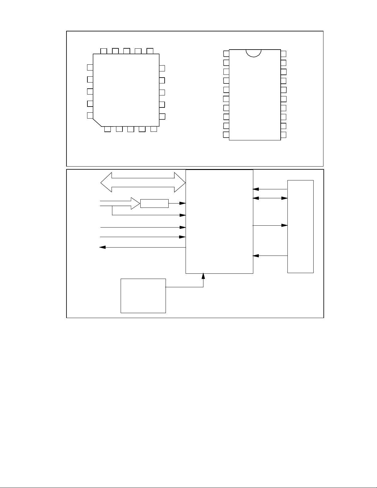
PIN CONFIGURATION
n
C
P
1
TXRXRSn
I
N
T
n
R
D
D
2
D3D
4
n
W
R
Package: 20 Pin PLCC
Package 20 Pin DIP
TTL CLOCK
TTL/RS-232-C
2
nCP
Vcc
0
D
D
1
nCS
DATA BUS
ADDRESS
BUS
nWRITE
nREAD
18 17 16 15 14
19
20
1
2
3
4 5 6 7 8
13
12
11
10
9
DECODE
CLOCK
D
7
D6
GND
D
5
D0-D7
nCS
RS
nWR
nRD
D
0
D1
nCS
nRD
2
D
D3
D4
nWR
D5
GND
10
COM81C17
TWENTY
PIN
UART
1
2
3
4
5
6
7
8
9
nCP1
nCP2
TX
20
19
18
17
16
15
14
13
12
11
Vcc
CP
2
CP
1
TX
RX
RS
nINT
CLOCK
D
7
D
6
INTERRUPT
REQUEST
nINT
RX
5.0688 MHZ
FIGURE 1 – TYPICAL TPUART INTERFACE
OSCILLATOR
OR
FIGURE 1 – TYPICAL TPUART INTERFACE
4
D0-D7
n
C
P
1
n
C
P
2
INTERNAL DATA BUS
220 OHM 30 pF 5.0688 MHz
nCS
nRD
nWR
RS
DATA
BUS
TRANS
READ
WRITE
DECODE
LOGIC
MODE
REGISTER
TRANSMIT
BUFFER
TRANSMIT
SHIFT REGISTER
TRANSMIT
CONTROL
TX
nINT
VCC
GND
MASK
REGISTER
& LOGIC
STATUS
REGISTER
CONTROL
REGISTER
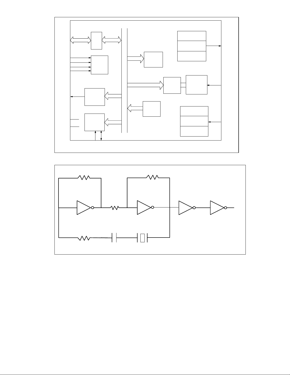
FIGURE 2 – COM81C17 BLOCK DIAGRAM
1800 OHM 560 OHM
220 OHM
7404 7404
BAUD
RATE
SELECT
REGISTER
BAUD
RATE
GENERATOR
RECEIVE
CONTROL
RECEIVE
SHIFT REGISTER
RECEIVE
BUFFER
7404 7404
CLOCK
RX
FIGURE 2A – 5.0688 MHz CRYSTAL OSCILLATOR CIRCUIT

5
DESCRIPTION OF PIN FUNCTIONS
DIP PIN NO. NAME SYMBOL
1, 2, 5-7,
9,11-12
DATA BUS D0-D7An 8-bit bi-driectional DATA BUS is used to
interface the TPUART to the processor Data Bus.
3 CHIP SELECT nCS A low level on this input enables the TPUART for
reading and writing to the processor. When nCS is
high, the DATA BUS is in high impedance and the
nWR and nRD will have no effect on the chip.
4 READ DATA
STROBE
nRD A low pulse on this input (when nCS is low) enables
the TPUART to place the data or the status
information on the DATA BUS.
8 WRITE DATA
STROBE
nWR A low pulse on this input (when nCS is low) enables
the TPUART to accept the data or control word
from the DATA BUS into the TPUART.
10 GROUND GND Power Supply Return.
13 CLOCK CLK External TTL Clock Input (See Table 2)
14 INTERRUPT
REQUEST
nINT An interrupt request is asserted by the TPUART
when an enabled condition has occurred in the
Status Register. This is an active low, open drain
output. This pin has an internal pullup register.
15 REGISTER
SELECT
RS During processor to TPUART communications, this
input is used to indicate which internal register will
be selected for access by the processor. When this
input is low, data can be written to the TX Holding
Buffer or data can be read from the RX Holding
Register. When this input is high control words can
be written to the Control Register or status
information can be read from the Status Register.
16 RECEIVER DATA RX This input is the receiver serial data. A high to low
transition is required to initiate data reception.
17 TRANSMITTER
DATA
TX This output is the transmitted serial data from the
TPUART. When a transmission is concluded, the
TX line will always return to the mark (High) state.
18 CONTROL PIN 1 nCP1 This control pin is an input only pin. It can be
programmed to perform the functions of CTS or
DSR/DCD.
19 CONTROL PIN 2 nCP2 This control pin can be programmed to be either an
input or an output. When in input mode, this pin
can perform the functions of DSR/DCD. When in
output mode, this pin can perform the functions of
DTR or RTS.
20 POWER SUPPLY V
+5V Supply Voltage
CC
DESCRIPTION

6
FUNCTIONAL DESCRIPTION
RESETTING THE TPUART
The TPUART must be reset on power up. Since
there is no external pin allocated for hardware
reset, this is accomplished by writing a One
(HIGH) followed by writing a Zero (LOW) to the
Command Register bit 7. Following reset, the
TPUART enters an idle state in which it can
neither transmit nor receive data.
INITIALIZING THE TPUART
The TPUART is initialized by writing three
control words from the processor. Only a single
address is set aside for Mode, Baud Rate
Select, Interrupt Mask and TX Buffer Registers.
For this to be possible, logic internal to the chip
directs information to its proper destination
based on the sequence in which it was written.
Following internal reset, the first write to address
zero (i.e. RS = 0) is interpreted as a Mode
Control word. The second write is interpreted as
Interrupt Mask word. The third write is
interpreted as Baud Rate Select. The fourth and
all subsequent writes are interpreted as writes to
the TX Buffer Register.
There is one way in which control logic may
return to anticipating a Mode, Interrupt Mask,
and Baud Rate Select words. This is following
an internal reset. Following initialization, the
TPUART is ready to communicate.
PROGRAMMABLE CONTROL PINS
The TPUART provides two programmable
control pins that can be configured to perform
as modem or terminal control handshake
signals. If no handshake signal is required,
these pins can be used as general purpose one
bit Input or Output ports.
nCP1 - is an input only pin that can be
programmed to act as the CTS (Clear To Send)
handshake signal, where it will disable data
transmission by the TPUART after the contents
of the Transmit Shift Register is completely
flushed out. When programmed as 1, nCP1 will
serve as a general purpose 1 bit input port. The
inverted state will be reflected in Status Register
bit 0 (when programmed as CTS or general
purpose input bit).
nCP2 - is an Input/Output pin. When configured
as Output, its state is directly controlled by the
host processor via writes to the Control
Register. This will serve the purpose of modem
and terminal handshake signals as RTS (Reset
To Send), and DTR (Data Terminal Ready).
When configured as Input, its inverted state is
reflected in the Status Register bit 1 and read by
the processor. This will serve the purpose of
handshake signals as DCD (Data Carrier
Detect) and DSR (Data Set Ready).
MODE REGISTER
BIT 1 BIT 2
0 0 nCP2 is RTS Output
0 1 nCP2 is GP Output
1 X nCP2 is GP Input
1 X nCP2 is GP Input
 Loading...