

Standard Microsystems Corporation COM20051I Datasheet

COM20051I
Integrated Microcontroller and
ARCNET (ANSI 878.1) Interface
FEATURES
!"
High Performance/Low Cost
!"
Microcontroller Based on Popular 8051
Architecture
!"
!"
!"
!"
!"
!"
!"
The COM20051I is a low-cost, highly-integrated microcontroller incorporating a high-performance network controller
based on the ARCNET Token Bus Standard (ANSI 878.1). The COM20051I is based around the popular Intel 8051
architecture. The device is implemented using a microcontroller core compatible with the Intel 80C32 ROMless
version of the 8051 architecture. The COM20051I is ideal for distributed control networking applications such as
those found in industrial/machine controls, building/factory automation, consumer products, instrumentation and
automobiles.
The COM20051I contains many features that are beneficial for embedded control applications. T he microcontroller is
a fully-functional 16MHz 80C32 that is comparable to the Intel 80C32 with 2 timers. In contrast to other embedded
controller/networking solutions, the COM20051I adds a fully-featured, robust, powerful, and simple network interface
while retaining all of the basic 8051 peripherals, such as the serial port and counter/timers.
In addition, the COM20051I supports an Emulation Mode that permits the use of a standard 80C32 emulator in
conjunction with the COM20051I to develop software drivers for the network core.
256-byte page of the External Data Memory Space of the 80C32. This provides for an easy interface between the
CPU and the ARCNET core.
that provides highly-reliable and fault tolerant message delivery at data rates ranging from 5Mbps down to 156
Kbps with message sizes varying from 0 to 507 bytes. The ARCNET protocol offers a simple, standardized, and
easily-understood networking solution for any application. The network interface supports several media interfaces,
including RS-485, coaxial, and twisted pair in either bus or star topologies. The network interface incorporates
powerful diagnostic features for network management and fault isolation. These include duplicate node ID detection,
reconfiguration detection, receive all (monitor) mode, receiver activity, and token detection.
8051 Instruction Set Compatible
Intel
Drop-In Replacement for 80C32 PLCC
Network Supports up to 255 Nodes
Powerful Network Diagnostics
Maximum 507 Byte Packets
Duplicate Node ID Detection
Self-Configuring Network Protocol
The networking core is based around an ARCNET Token Bus protocol engine
GENERAL DESCRIPTION
ORDERING INFORMATION
Order Number: COM20051ILJ P
44 Pin PLCC Package
!"
Retains all 8051 Peripherals Including Serial I/O
and Two Timers
!"
Utilizes ARCNET Token Bus Network Engine
!"
Requires No Special Emulators
!"
5 Mbps to 156 Kbps Network Data Rate
!"
Network Interface Supports RS-485, Twisted Pair,
Coaxial, and Fiber Optic Interfaces
!"
Receive All Mode Allows Any Packet to Be
Received
ARCNET core is mapped to a
SMSC DS – COM20051I Rev. 03/27/2000

© STANDARD MICROSYSTEMS CORPORATION (SMSC) 2000
80 Arkay Drive
Hauppauge, NY 11788
(631) 435-6000
FAX (631) 273-3123
Standard Microsystems is a registered trademark of Standard Microsystems Corporation, and SMSC is a trademark of Standard Microsystems
Corporation. Product names and company names are the trademarks of their respective holders. Circuit diagrams utilizing SMSC products are
included as a means of illustrating typical applications; consequently complete information sufficient for construction purposes is not necessarily given.
Although the information has been checked and is believed to be accurate, no responsibility is assumed for inaccuracies. SMSC reserves the ri ght to
make changes to specifications and product descriptions at any time without notice. Contact your local SMSC sales office to obtain the latest
specifications before placing your product order. The provision of this information does not convey to the purchaser of the semiconductor devices
described any licenses under the patent rights of SMSC or others. All sales are expressly conditional on your agreement to the terms and conditions of
the most recently dated version of SMSC's standard Terms of Sale Agreement dated before the date of your order (the "Terms of Sale Agreement").
The product may contain design defects or errors known as anomalies which may cause the product's functions to deviate from published
specifications. Anomaly sheets are available upon request. SMSC products are not designed, intended, authorized or warranted for use in any life
support or other application where product failure could cause or contribute to personal injury or severe property damage. Any and all such uses
without prior written approval of an Officer of SMSC and further testing and/or modification will be fully at the risk of the customer. Copies of this
document or other SMSC literature, as well as the Terms of Sale Agreement, may be obtained by visiting SMSC’s website at http://www.smsc.com.
SMSC DISCLAIMS AND EXCLUDES ANY AND ALL WARRANTIES, INCLUDING WITHOUT LIMITATION ANY AND ALL IMPLIED WARRANTIES
OF MERCHANTABILITY, FITNESS FOR A PARTICULAR PURPOSE, TITLE, AND AGAINST INFRINGEMENT, AND ANY AND ALL
WARRANTIES ARISING FROM ANY COURSE OF DEALING OR USAGE OF TRADE.
IN NO EVENT SHALL SMSC BE LIABLE FOR ANY DIRECT, INCIDENTAL, INDIRECT, SPECIAL, PUNITIVE, OR CONSEQUENTIAL DAMAGES,
OR FOR LOST DATA, PROFITS, SAVINGS OR REVENUES OF ANY KIND; REGARDLESS OF THE FORM OF ACTION, WHETHER BASED ON
CONTRACT, TORT, NEGLIGENCE OF SMSC OR OTHERS, STRICT LIABILITY, BREACH OF WARRANTY, OR OTHERWISE; WHETHER OR
NOT ANY REMEDY IS HELD TO HAVE FAILED OF ITS ESSENTIAL PURPOSE; AND WHETHER OR NOT SMSC HAS BEEN ADVISED OF THE
POSSIBILITY OF SUCH DAMAGES.
SMSC DS – COM20051I Page 2 Rev. 03/27/2000

TABLE OF CONTENTS
FEATURES................................................................................................................................................................... 1
GENERAL DESCRIPTION............................................................................................................................................ 1
PIN CONFIGURATION ................................................................................................................................................. 4
OVERVIEW................................................................................................................................................................... 5
DESCRIPTION OF PIN FUNCTIONS........................................................................................................................... 5
BASIC ARCHITECTURE............................................................................................................................................... 8
PROTOCOL DESCRIPTION....................................................................................................................................... 13
NETWORK PROTOCOL............................................................................................................................................. 13
DATA RATES.............................................................................................................................................................. 13
NETWORK RECONFIGURATION..............................................................................................................................13
BROADCAST MESSAGES......................................................................................................................................... 15
EXTENDED TIMEOUT FUNCTION............................................................................................................................ 15
LINE PROTOCOL ....................................................................................................................................................... 15
SYSTEM DESCRIPTION............................................................................................................................................18
MICROCONTROLLER INTERFACE........................................................................................................................... 18
TRANSMISSION MEDIA INTERFACE........................................................................................................................18
ARCNET CORE FUNCTIONAL DESCRIPTION.........................................................................................................23
MICROSEQUENCER.................................................................................................................................................. 23
INTERNAL REGISTERS............................................................................................................................................. 23
INTERNAL RAM.......................................................................................................................................................... 35
SOFTWARE INTERFACE........................................................................................................................................... 35
COMMAND CHAINING............................................................................................................................................... 38
RESET DETAILS......................................................................................................................................................... 40
INITIALIZATION SEQUENCE..................................................................................................................................... 40
IMPROVED DIAGNOSTICS........................................................................................................................................ 41
COM20051I APPLICATIONS INFORMATION............................................................................................................ 43
USING ARCNET DIAGNOSTICS TO OPTIMIZE YOUR SYSTEM............................................................................. 60
CABLING THE COM20051I........................................................................................................................................64
USING THE COM20051I'S EMULATION MODE........................................................................................................ 65
OPERATIONAL DESCRIPTION.................................................................................................................................. 66
MAXIMUM GUARANTEED RATINGS........................................................................................................................ 66
DC ELECTRICAL CHARACTERISTICS ..................................................................................................................... 66
TIMING DIAGRAMS.................................................................................................................................................... 68
PACKAGE DIMENSIONS ........................................................................................................................................... 74
SMSC DS – COM20051I Page 3 Rev. 03/27/2000
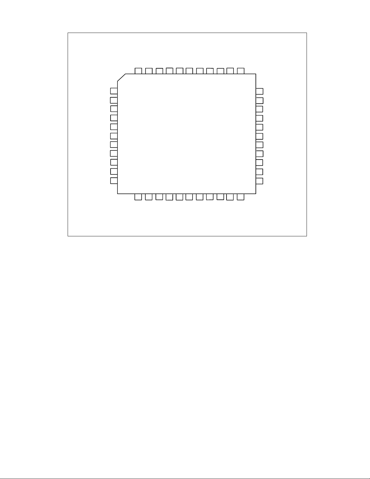
PIN CONFIGURATION
P1.4
P1.3
P1.2
P1.1
P1.0
RXIN
VCC
P0.0/AD0
P0.1/AD1
P0.2/AD2
6 5 4 3 2 1 44 43 42 41 40
P0.3/AD3
P1.5
P1.6
P1.7
RST
P3.0/RXD
nPULSE1
P3.1/TXD
P3.2/INT0
P3.3/INT1
P3.4/T0
P3.5/T1
7
8
9
10
11
12
13
14
15
16
17
COM20051I
COM20051
18 19 20 21 22 23 24 25 26 27 28
VSS
XTAL2
P3.6/nWR
XTAL1
P3.7/nRD
nPULSE2
P2.0/A8
P2.1/A9
39
38
37
36
35
34
33
32
31
30
29
P2.2/A10
P2.3/A11
P2.4/A12
P0.4/AD4
P0.5/AD5
P0.6/AD6
P0.7/AD7
nEA/EMUL
TXEN
ALE
nPSEN
P2.7/A15
P2.6/A14
P2.5/A13
SMSC DS – COM20051I Page 4 Rev. 03/27/2000

OVERVIEW
The COM20051I is essentially a network board-in-a-chip. It takes an 80C32 microcontroller core and an ARCNET
controller and integrates them into a single device. ARCNET is a token passing-based protocol that combines
powerful flow control, error detection, and diagnostic capabilities to deliver fast and reliable messages. The
COM20051I supports a variety of data rates (5 Mbps to 156 Kbps), topologies (bus, star, tree), and media types (RS485, coax, twisted pair, fiber optic, and powerline) to suit any type of application.
The ARCNET network core of the COM20051I contains many features that make network development simple and
easy to comprehend. Diagnostic features, such as Receive All, Duplicate ID Detection, Reconfiguration Detection,
Token, and Receiver Detection, all combine to make the COM20051I simple to use and to implement in any
environment. The ARCNET protocol itself is relatively simple to understand and very flexible. A wide variety of
support products are available to assist in network development, such as software drivers, line drivers, boards, and
development kits. The COM20051I implements a full-featured 16MHz, Intel-compatible 80C32 microcontroller with all
of the standard peripheral functions, including a full duplex serial port, two timer/counters, one 8-bit general purpose
digital I/O port, and interrupt controller. The 8051 architecture has long been a standard in the embedded control
industry for low-level data acquisition and control. ARCNET and the 8051 form a si mple solution for many of today's
and tomorrow's low-level networking solutions.
In addition to the 80C32 and the ARCNET network core, the COM20051I contains all the address decoding and
interrupt routing logic to interface the network core to the 80C32 core. The integrated 8051/ARCNET combination
provides an extremely cost-effective and space-efficient solution for industrial networking applications. The
COM20051I can be used in a stand-alone embedded application, executing control algorithms or performing data
acquisition and communicating data in a master/slave or
handling communication tasks in a multi-processing system.
peer-to-peer
configuration, or used as a slave processor
DESCRIPTION OF PIN FUNCTIONS
PIN NO. NAME SYMBOL DESCRIPTION
1 Receive In RXIN Input. Network receiver input.
2-9 P1.0-1.7 P1.0-1.7 Input/Output. Port 1 of the 8051. General purpose
digital I/O port.
10 Reset RESET Input. Active high reset.
11 P3.0 P3.0 Input/Output. Port 3 bit 0 of the 8051. RX input of
serial port.
12 nPulse 1 nPULSE1 Output. Network output. Open-drain when
backplane mode is invoked, otherwise it is a push-
pull output.
13-19 P3.1-3.7 P3.1-3.7 Input/Output. Port 3 bits 1-7 of the 8051.
20, 21 Crystal Oscillator XTAL1,
XTAL2
22 Ground VSS Ground pin.
23 nPulse 2 nPULSE2 Output. Network output. Outputs a synchronous
24-31 P2.0-2.7 P2.0-2.7 Input/Output. Port 2 of the 8051. High order address
32 nProgram Store
Enable
33 Address Latch
Enable
34 Transmit Enable TXEN Output. This signal is used to enable the drivers for
nPSEN Output.
ALE Output.
Input. Oscillator inputs 1 and 2.
clock at 2x the data rate when backplane mode is
invoked.
bus.
transmitting. The polarity of this signal is
programmable by grounding the nPULSE2 pin prior
to the POWER-UP.
nPULSE2 floating prior to the power-up = TXEN
active high
nPULSE2 grounded prior to the power-up = TXEN
active low. (This option is available only in the
Backplane mode).
SMSC DS – COM20051I Page 5 Rev. 03/27/2000
DESCRIPTION OF PIN FUNCTIONS
(
)
PIN NO. NAME SYMBOL DESCRIPTION
35 nEnable nEA Input. When high, causes the 8051's outputs to tri-
state. When low, allows the 8051 to address external
memory. Must be low to execute code from the
embedded 8051.
36-43 P0.7-0.0 P0.7-0.0 Input/Output. Port 0 of the 8051. Multiplexed low
order address/data bus.
44 Power Supply VCC +5V power supply.
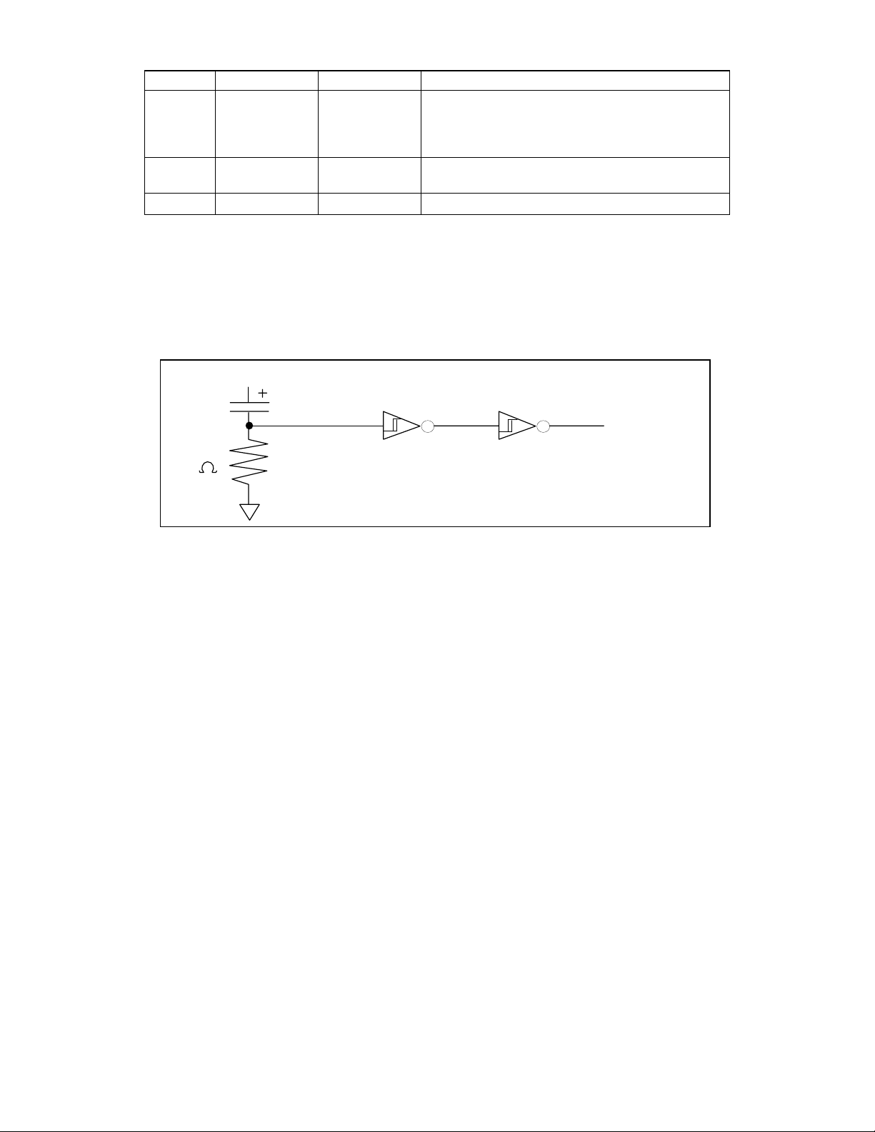
RESET CIRCUIT FOR THE COM20051I
The power on reset circuit for the COM20051I should be designed to provide a clean, fast transition time TTL input to
the COM20051I. Sufficient signal high time on RST (pin 10) should be provided after Vcc reaches +5V DC. The
following circuit, which provides an 8ms power-on reset pulse, is recommended:
Vcc (+5V)
22uF/
10V
RST
PIN 10
220
74LS14
SMSC DS – COM20051I Page 6 Rev. 03/27/2000
EMULALE
CONTROL
BUS
ALE
nPSEN
80C32
PORT1
PORT0
TX
RX
PORT3
T0
T1
PORT2
A8-A15
INT 0 INT1
FIGURE 1 – INTERNAL ARCHITECTURE OF THE COM20051I
ALE
ARCNET CORE (COM20010)
AD0-AD7
ADDRESS
DECODER
INTERRUPT
ROUTER
IN T 0 IN T1
IN TnCSRD/WR
nPULSE1
nPULSE2
TXEN
RXIN
SMSC DS – COM20051I Page 7 Rev. 03/27/2000

BASIC ARCHITECTURE
The COM20051I consists of four functional blocks: the 80C32 microcontroller core, ARCNET network cell (includes
1K of buffer RAM), programmable address decoder, and programmable interrupt router. The internal architecture of
the COM20051I is shown in Figure 1.
The 80C32 microcontroller is a full ROMless implementation of the popular Intel 8051 series. The ARCNET network
core is similar in arc hitecture to SMSC's popular COM20020 family of ARCNET controllers and retains the same
command and status flags of previous ARCNET controllers. The programmable address decoder maps the ARCNET
registers into a 256-byte page anywhere within the External Data Memory space of the 80C32. The ARCNET core
was mapped to the External Data Memory space to simplify software and application development and for
production test purposes.
ARCNET core is available to the developer when working with the 8051 emulator.
When
the COM20051I is put into Emulate mode, the internal microcontroller is put into a high impedance state, thus
allowing an external In-Circuit Emulator (ICE) to program the ARCNET core. The advantage of this approach versus
mapping the ARCNET registers into the internal memory (Special Function) area of the 80C32 is that dedicated
software development tools will not be necessary to debug application software. Since a majority of 8051
applications use only a small portion of the Data Memory space, there is no penalty paid for used address space.
There will also be no penalty in execution time, since cycle times for external data memory accesses and internal
direct memory moves are identical. The network interrupt can be routed to either of the two external interrupt ports or
can be assigned to one of the general purpose I/O ports. The ARCNET interrupt is internally wire ORed with the
external interrupt pin to allow greater system flexibility.
80C32 ARCHITECTURE AND INSTRUCTION SET
The 80C32 microcontroller core is identical to the 16MHz Intel 80C32 in all respects
2.
Please refer to the Intel Embedded Microcontrollers and Processors Databook
except for the absence of Timer
, Volume 1, for details regarding
the 8051 architecture, peripherals, instruction set, and programming guide. Note that any access to the internal
ARCNET core or any external memorry access is
visible
on the pins of the COM20051I.
The following differences apply to the COM20051I:
1. Oscillator frequency is 40MHz instead of 16MHz. This is necessary to derive a 20MHz clock for the ARCNET
core. The processor still operates at 16MHz.
2. nEA pin - This pin must be tied to ground for normal internal processor operation. When tied to VCC, the
COM20051I will enter the Emulate mode.
3. Unused pins - The COM20051I is packaged in a 44-pin PLCC. Network I/O is generated on the four unused pins
of the standard 80C32 PLCC package. No DIP package is available.
4. Power Down operation - The Power Down mode can only be used in conjunction when the internal oscillator is
being used. If an external oscillator is used and the Power Down mode is invoked, damage may result to the
oscillator and to the COM20051I.
Clock Speed
The COM20051I processor operates at 16MHz and the network controller at a maximum 40MHz clock rate. A single
crystal oscillator is used to supply the two clocks: a 16MHz processor clock and a 20MHz network clock for the
nominal 2.5 Mbps data rate. Pins 20 and 21 are designated as crystal inputs. When clocking with an external
oscillator, pin 21 (XTAL1) functions as the clock input.
Emulate Mode
The COM20051I contains a unique feature called the Emulate mode that most 8051-based peripheral devices do
not accommodate. TheEmulate mode permits developers to access and program the internal ARCNET core using a
standard low-cost 8032 emulator. This feature eliminates the need for expensive dedicated development equipment
needed for other types of 8051-based peripheral devices. The Emulate mode is invoked by connecting the nEA pin
to VCC. This causes the internal 80C32 processor to enter a HI-Z state and changes the state of the COM20051I
pins according to the following table:
SMSC DS – COM20051I Page 8 Rev. 03/27/2000

Table 1 - Emulate Mode
SIGNAL NAME EMUL = 0 EMUL = 1
PORT 0 Bidirectional Bidirectional
PORT 1 Bidirectional HI-Z (except for pins
designated as interrupt
destinations)
PORT 2 Output Input
INT0,1
Input Output
(P3.2, P3.3)
RD/WR
Output Input
(P3.6, P3.7)
ALE Output Input
TX,T0, T1
Output HI-Z
(P3.1,3.4,3.5)
nPSEN
Address Decoding
The COM20051I, as described previously, maps the ARCNET registers into the 80C32's External Data Memory
space. This provides system flexibility because the location of the ARCNET registers can be located anywhere within
the 64K External Data Memory space. The precise location can be resolved with a 256-byte page. The location of
that page in the External Data Memory space is pointed to by the
read/write
Address Decode Register, as shown in
Figure 2. The Address Decode Register is located at FFFFh of the External Data Memory space. It holds the upper
8 bits of the 16-bit address at which the 256 page boundary will start. This register must be programmed prior to any
access to the ARCNET core. The default value is 0000h.
The ARCNET core register page must be mapped away from the external RAM prior to any access to the external
RAM by the software. Failure to do this may result in incorrect data write and read operations to the external RAM as
well as the core registers.
SMSC DS – COM20051I Page 9 Rev. 03/27/2000
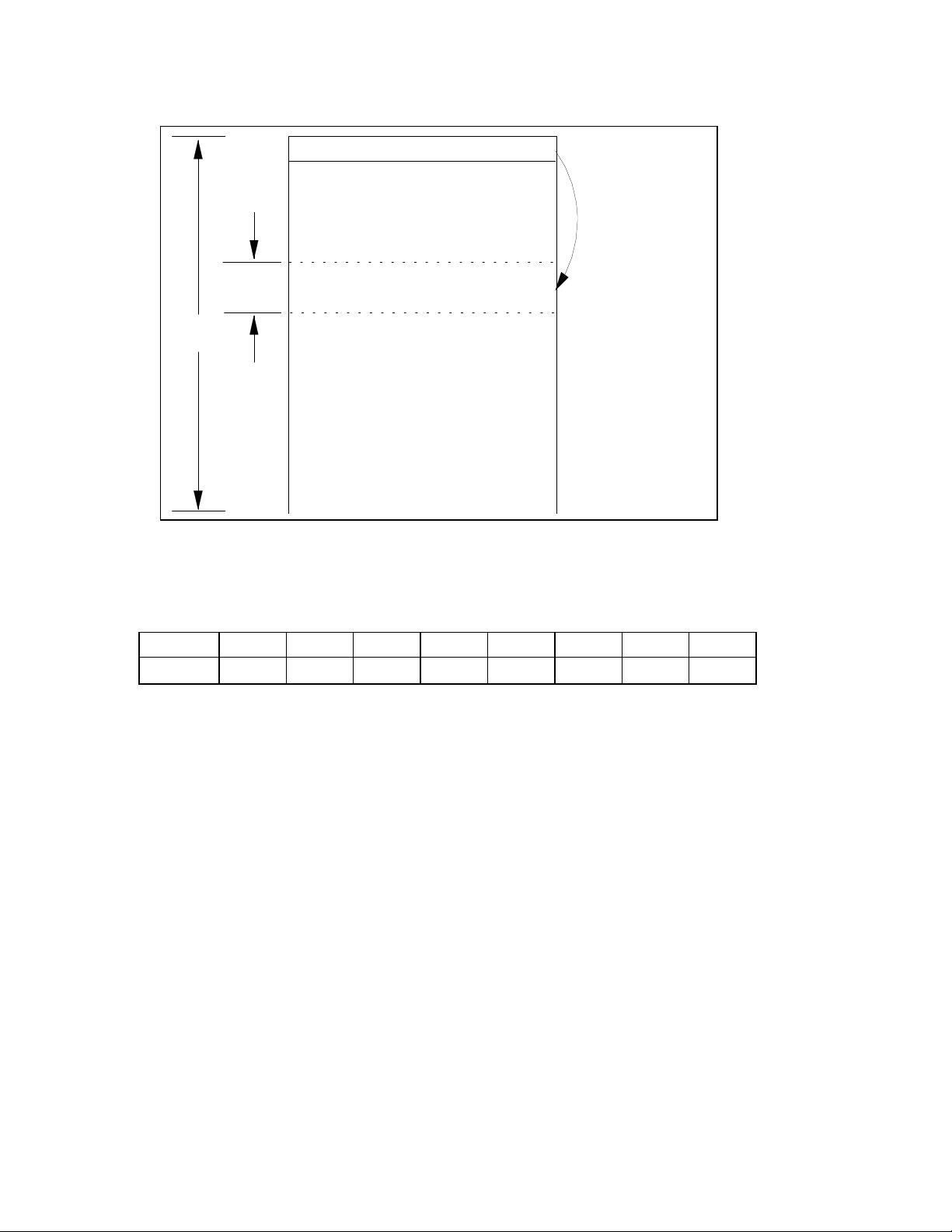
FFFFh
ADDRESS DECODE
REGISTER
(FIXED LO C ATION)
V ALU E x 10 0h
256 BYT ES
64K
BYTES
ARCNET CORE
PAGE
LOCATION CAN
VARY
0000h
FIGURE 2 – COM20051I EXTERNAL DATA ADDRESS SPACE
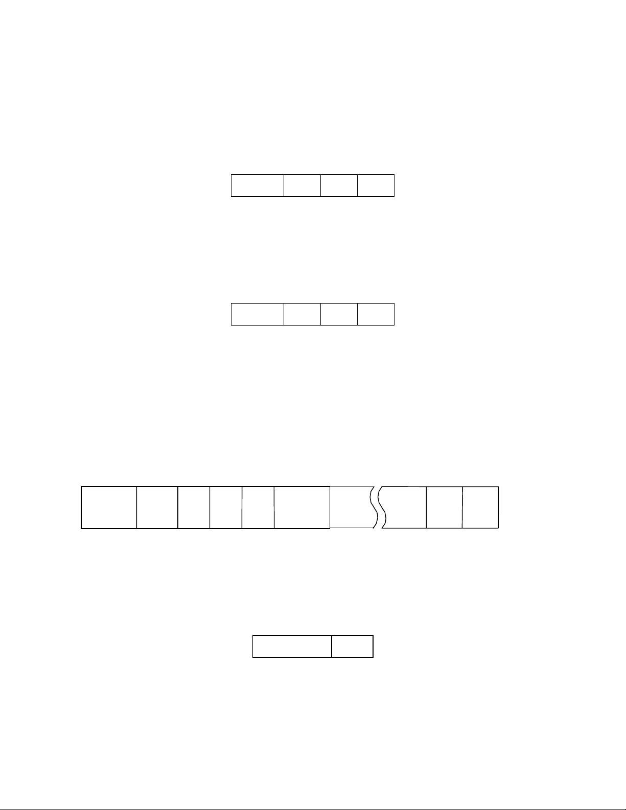
ADDRESS DECODE REGISTER
NAME BIT 7 BIT 6 BIT 5 BIT 4 BIT 3 BIT 2 BIT 1 BIT 0
ADR DEC A15 A14 A13 A12 A11 A10 A9 A8
LOCATION: FFFFh of the External Data Memory space. Default: 00h
EXAMPLE: Address Decode Register = 80h
ARCNET core registers
Configuration Register offset = 06h, physical address = 8006h).
will be located at 8000h + Register offset (e.g. ARCNET
SMSC DS – COM20051I Page 10 Rev. 03/27/2000

COM20051I MEMORY MAPPING
The COM20051I maps the Arcnet core into a 256 byte page of data memory space. This memory is physically
located internally to the device and itrquote s default base address on power up is 0000h. This 256 byte page can be
logically located anywhere within the 64K external data memory space while physically remaining on board. The
location of this 256 byte page is pointed to by the Address Decode Register in the device. This Address Decode
Register holds the upper 8 bits of the 16 bit address at which the 256 byte page boundary will start. The address of
this Address Decode Register is FFFFh. This register is also logically located in external data memory space but
physically located on the device. This register must be written to on power-up to properly locate the Arcnet core. .
The user must ensure that the Arcnet corerquote s 256 byte page does not conflict with external memory, otherwise
data bus contention will result. As an example, if the user has 32K of external data memory located from 0000h to
7FFFh then the Arcnet core should be mapped above this area, 8000H is suggested. The user will write 80h to
address FFFFh on power up to properly map the core to this location.
ARCNET Network Core - Overview and Architecture
ARCNET is a baseband token passing network protocol (ANSI 878.1). ARCNET features deterministic behavior,
hardware-based network configuration, flexible topologies, several data rates, and multiple media support. Data
rates varying from 5 Mbps to 156 Kbps and message sizes from 0 to 507 bytes are supported. Supported media
includes RS-485, twisted pair, coax, fiber optic, and powerline in bus, star or tree topologies. ARCNET has enjoyed
widespread use in the industrial community, finding a home in such applications as I/O control/acquisition, multiprocessor communications, point-of-sale terminals, in-vehicle navigation systems, data acquisition systems, remote
sensing, avionics, machine control, embedded computing, building automation, robotics, consumer products, and
security systems.
The ARCNET core used in the COM20051I is similar in architecture to SMSC's 200XX series of Industrial ARCNET
Controllers. The ARCNET core of the COM20051I contains a 1K x 8 internal RAM for packet buffering, Duplicate ID
Detection, Receive All Mode, New Next ID Indicator, Excessive NACK Interrupt, Programmable Data Rates,
Backplane Mode, Programmable Transmitter Enable, Polarity Receive Activity, Reconfiguration, Token Seen
Indicators, and Network Mapping hooks. The ARCNET core of the COM20051I uses a software-programmable node
enabling the user to program the Node ID according to the application needs. The Node ID can be stored in an
ID,
electronic medium or changed with the switch.
SMSC DS – COM20051I Page 11 Rev. 03/27/2000
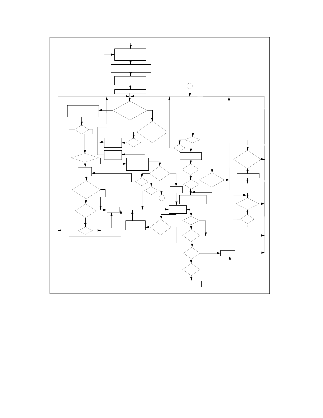
Power On
Start
Reconfiguration
Time r (8 40 m S)
Reconfigure
Timer has
Timed Out
Y
Send
Reconfigure
Burst
Read Node ID
Write ID to
RAM Buffer
Set NID=ID
Invitation
to Transmit to
this ID?
N
YN
TA?
Broadcast?
Y
Send
Packet
Was Packet
Broadcast?
N
No
Y
Activity
for 74.7
us?
N
Y
N
ACK? Set TMA
YN
Trans mi t
NAK
Trans mit
ACK
N
Y
Set TA
YN
RI?
Trans mit
Free Buffer
Enquiry
YN
ACK?
NID
Free Buff er
Enquiry to
this ID?
N
Y
NAK?
No
Activity
for 74.7
us?
N
No
Activity
for 74.7
us?
1
ID refers to the identification number of the ID assigned to this node.
NID ref e rs to th e n e x t ide n tification nu mber that r ec e iv es the to ke n a fter
after this ID p a s se s it.
SID ref er s to the s ou r ce ide n tification .
DID refers to the destination identification.
-
SOH refers to the start of header character; preceeds all data packets.
-
Note*: Time values pertain to the default 2.5 Mbps operation
FIGURE 3 - DETAILED ARCNET CORE OPERATION
Y
Set TA
Pass the
Token
NYIncrement
RI?
1
YN
SOH?
NY
Write SID
to B uffer
Y
DID
=0?
N
Broadcast
DID
=ID?
Y
Write Buffer
with Packet
CRC
OK?
LENGTH
OK?
DID
=0?
N
DID
=ID?
Y
SEND ACK
Enabled?
N
N
Y
N
Y
Y
N
No Activity
for 82
uS?
Set NID=ID
N
Y
Set RI
Start Time r:
T=(255-ID)
x 146 us
Activity
On Line?
N
T=0?
N
Y
Y
N
Y
SMSC DS – COM20051I Page 12 Rev. 03/27/2000

PROTOCOL DESCRIPTION
NETWORK PROTOCOL
Communication on the network is based on a token passing protocol. Establishment of the network configuration
and management of the network protocol are handled entirely by
called ARCNET network core .
The 80C32 controller core transmits data by simply loading a data packet and its
destination ID into the network core's RAM buffer, and issuing a command to enable the transmitter. When the
ARCNET core next receives the token, it verifies that the receiving node is ready by first transmitting a FREE
BUFFER ENQUIRY message. If the receiving node transmits an ACKnowledge message, the data packet is
transmitted followed by a 16-bit CRC. If the receiving node cannot accept the packet (typically its receiver is
inhibited), it transmits a Negative AcKnowledge message and the transmitter passes the token. Once it has been
established that the receiving node can accept the packet and transmission is complete, the receiving node verifies
the packet. If the packet is received successfully, the receiving node transmits an ACKnowledge message (or
nothing if it is not received successfully) allowing the transmitter to set the appropriate status bits to indicate
successful or unsuccessful delivery of the packet. An interrupt mask permits the ARCNET core to generate an
interrupt to the processor when selected status bits become true. Figure 4 is a flow chart illustrating the internal
operation of the ARCNET core.
data rate.
All timing details in th e discuss ion of ARCNET protocol are based on the 2.5 Mbps
DATA RATES
The ARCNET core is capable of supporting data rates from 156.25 Kbps to 5 Mbps. For slower or faster data rates,
an internal Programmable clock divider scales down the clock frequency. Thus all timeout values are scaled up
as shown in the following table:
DATA
CLOCK
PRE-
SCALER
8
!
16
!
32
!
64
!
128
!
40 MHz CLOCK
DIV. TO 20 MHz
25Mbps
1.25Mbps
625Kbps
3125Kbps
156.25
Kbps
RATE
40 MHz UN-
DIVIDED
5Mbps
25Mbps
1.25Mbps
625Kbps
3125Kbbps
the COM20051I's internal microcoded sequencer
TIMEOUT SCALING
FACTOR
(MULTIPLY BY)
40 MHz CLOCK
DIV. TO 20 MHz
1
2
4
8
16
40 MHz UN-
DIVIDED
.5
1
2
4
8
NETWORK RECONFIGURATION
A significant advantage of the ARCNET is its ability to adapt to changes on the network. Whenever a new node is
activated or deactivated, a NETWORK RECONFIGURATION is performed. When a new ARCNET node is turned on
(creating a new active node on the network), or if the COM20051I has not received an INVITATION TO TRANSMIT
for 840ms, or if a software reset oc curs, the ARCNET node causes a NETW ORK RECONFIGURATION by sending
a RECONFIGURE BURST consisting of eight marks and one space repeated 765 times. The purpose of this burst is
to terminate all activity on the network. Since this burst is longer than any other type of transmission, the burst will
interfere with the next INVITATION TO TRANSMIT, destroy the token and keep any other node from assuming
control of the line.
When any ARCNET node senses an idle line for greater than 82 S, which occurs only when the token is lost, it starts
an internal timeout equal to 146 s times the quantity 255 minus its own ID.
reconfiguration by sending an invitation to transmit (TOKEN) first to itself and then to
The COM20051I starts network
all other nodes by
incrementing the destination Node ID value. If the timeout expires with no line activity, the ARCNET core starts
sending INVITATION TO TRANSMIT with the Destination ID (DID) equal to the currently stored NID. Within a given
network, only one node will timeout (the one with the highest ID number). After sending the INVITATION TO
TRANSMIT, the COM20051I waits for activity on the line. If there is no activity for 74.7 S, the COM20051I
increments the NID value and transmits another INVITATION TO TRANSMIT using the NID equal to the DID. If
activity appears before the 74.7 S timeout expires, the COM20051I releases control of the line. During NETWORK
RECONFIGURATION, INVITATIONS TO TRANSMIT are sent to all NIDs
(1-255).
SMSC DS – COM20051I Page 13 Rev. 03/27/2000
HARDWARE OR
SOFTWARE RES ET
OR NO TOKEN FOR
840 MS
NODE DRO PS
OFF TH E
NETWORK
SEND RECON
BURST
(765 times 111111110)
TIMEOUT FOR
146µs x
(255 - NODE ID)
NO ACTIVITY
WITHIN 82µs?
N
Y
TRANSMIT TOKEN
TO NODE = OWN ID
LINE ACTIVITY
DETECTED
WITHIN 7 4 .7µs
N
Y
N
SET RECON BIT
IN THE STATUS
REGISTER &
NEW NEXT ID
BIT IN THE
DIAGNOSTIC
STATUS
REGISTER
END NO DE
RECONFIGURATION
INCREMENT TOKEN
VALUE AND
TRANSMIT
FIGURE 4 - ARCNET RECONFIGURATION PROCESS
840ms
TIMER
EXPIRED?
Y
SMSC DS – COM20051I Page 14 Rev. 03/27/2000

Each COM20051I on the network will finally have saved a NID value equal to the ID of the ARCNET node that it
released control to. This is called the Next ID Value. At this point, control is passed directly from one node to the
next with no wasted INVITATIONS TO TRANSMIT being sent to ID's not on the network, until the next NETWORK
RECONFIGURATION occurs. W hen a node is powered off, the previous node attempts to pass the token to it by
issuing an INVITATION TO TRANSMIT. Since this node does not respond, the previous node times out and
transmits another INVITATION TO TRANSMIT to an incremented ID and eventually a response will be received.
The NETWORK RECONFIGURATION time depends on the number of nodes in the network, the propagation delay
between nodes, and the highest ID number on the network, but is typically within the range of 24 to 61 ms for 2.5
Mbps operation.
BROADCAST MESSAGES
Broadcasting gives a particular node the ability to transmit a data packet to all nodes on the network simultaneously.
NID=0
is reserved for this feature and no node on the network can be assigned
the transmitting node's processor simply loads the RAM buffer with the data packet and sets the DID
equal to zero. Figure 12 illustrates the position of each byte in the packet with the DID residing at address
NID=0.
To broadcast a message,
(Destination ID)
1Hex
of
the current page selected in the "Enable Transmit from Page fnn" command. Each individual node has the ability to
ignore broadcast messages by setting the most significant bit of the "Enable Receive to Page fnn" command (see
Table 8) to a logic "0".
EXTENDED TIMEOUT FUNCTION
There are three timeouts associated with the COM20051I operation. The values of these timeouts are controlled by
bits 3 and 4 of the Configuration Register
and bit 5 of the Setup Register (see register description for details).
Response Time
(ET1, ET2)
The Response Time determines the maximum propagation delay allowed between any two nodes, and should be
chosen to be larger than the round trip propagation delay between the two furthest nodes on the network plus the
maximum turn around time (the time it takes a partic ular ARCNET node to start sending a message in respons e to a
received message) which is approximately 12.7 S. The round trip propagation delay is a function of the transmission
media and network topology. For a typical system using RG62 coax in a baseband system, a one way cable
propagation delay of 31 S translates to a distance of about 4 miles. The flow chart in Figure 3 uses a value of 74.7 S
(31 + 31 + 12.7) to determine if any node will respond.
Idle Time
(ET1, ET2)
The Idle Time is associated with the NETWORK RECONFIGURATION. Figure 3 and Figure 4 illustrate that during a
NETWORK RECONFIGURATION one node will continually transmit INVITATIONS TO TRANSMIT until it
encounters an active node. All other nodes on the network must distinguish between this operation and an entirely
idle line. During NETW ORK RECONFIGURATION, activity will appear on the line every 82 S. This 82 S is equal to
the Response Time of 74.7 S plus the time it takes the COM20051I to start retransmitting another message (usually
another INVITATION TO TRANSMIT).
Reconfiguration Time
(ET1, ET2)
If any node does not receive the token within the Reconfiguration Time, it will initiate a NETWORK
RECONFIGURATION. The ET2 and ET1 bits of the Configuration Register allow the network to operate over longer
distances than the 4 miles stated earlier. The logic levels on these bits control the maximum distances over which
the COM20051I can operate by controlling the three timeout values described above. For proper network operation,
all nodes connected to the same network must have the same Response Time, Idle Time, and Reconfiguration Time.
LINE PROTOCOL
The ARCNET line protocol is considered isochronous because each byte is preceded by a start interval and ended
with a stop interval. Unlike asynchronous protocols, there is a constant amount of time separating each data byte.
Each byte takes exactly 11 clock intervals that are defined by nPULSE1 and nPULSE2 signals (at 2.5 Mbps one byte
takes 4.4 ms). As a result a time to transmit a message can be precisely determined. The line idles in a spacing
(logic "0") condition. A logic "0" is defined as no line activity and a logic "1" is defined as a negative pulse of 200nS
duration.
SMSC DS – COM20051I Page 15 Rev. 03/27/2000
A transmission starts with an ALERT BURST consisting of 6 unit intervals of mark (logic "1"). Eight bit data
characters are then sent, with each character preceded by 2 unit intervals of mark and one unit interval of space.
Five types of transmission can be performed as described below:
Invitations To Transmit
An Invitation To Transmit is used to pass the token from one node to another and is sent by the following sequence:
!"
An ALERT BURST
!"
ITT (Invitation To Transmit:
An
!"
Two (repeated) DID (Destination ID) characters
Free Buffer Enquiries
A Free Buffer Enquiry is used to ask another node if it is able to accept a packet of data. It is sent by the following
sequence:
!"
!"
!"
Data Packets
A Data Packet consists of the actual data being sent to another node. It is sent by the following sequence:
!"
!"
!"
!"
!"
!"
!"
An ALERT BURST
An FBE - Free Buffer Enquiry: ASCII code 85H)
Two (repeated) DID (Destination ID) characters
(PAC)
An ALERT BURST
PAC (Data Packet
An
An SID (Source ID) character
Two (repeated) DID (Destination ID) characters
A single COUNT character which is the 2's complement of the number of data bytes to follow if a short
packet is sent, or 00
N data bytes where COUNT = 256-N (or 512-N for a long packet)
Two CRC (Cyclic Redundancy Check) characters. The CRC polynomial used is: X16 + X15 + X2 + 1.
(ITT)
ASCII code 04H)
(FBE)
--ASCII code 01H)
Hex
followed by a COUNT character if a long packet is sent
ALERT
BURST
ALERT
BURST
ITT
FBE
DID DID
DID DID
ALERT
BURST
Acknowledgements
An Acknowledgement is used to acknowledge reception of a packet or as an affirmative response to FREE BUFFER
ENQUIRIES and is sent by the following sequence:
!"
An ALERT BURST
!"
An ACK (ACKnowledgement--ASCII code 86H) character
SMSC DS – COM20051I Page 16 Rev. 03/27/2000
PAC
(ACK)
SID
DID
DID
ALERT
BURST
COUNT
data
ACK
data
CRC
CRC
Negative Acknowledgements
A Negative Acknowledgement is used as a negative response to FREE BUFFER ENQUIRIES and is sent by the
following sequence:
!"
An ALERT BURST
!"
A NAK (Negative Acknowledgement--ASCII code 15H) character
Figure 5 illustrates the flow of events on a 5-node network where a node with the NID=1 transmits a data packet to
a node with the NID=5, and a node with the NID=3 tries to transmit a data to a node with the NID=4 but node 4
cannot accept it. All other nodes are just passing the tokens.
(NAK)
ALERT
BURST
NAK
#5
ITT to #1
#1 FBE to #5 #5 ACK to #1 #1
PAC t o #5
#5 ACK to #1
#3 ITT to #4
#4 NAK to #3
#3 FBE to #4
#1 ITT to #2#2 ITT to #3
#4 ITT to # 5
SEQUENC E O F L INE EVENTS
1) NODE 1 RECEIVES TOKEN FR OM NOD E 5
2) NODE 1 TRANSM ITS TO NODE 5
A) ISSUES FBE TO NOD E 5
B) NODE 5 IS READ Y TO R ECEIVE SO IT ISSUES AN ACK
C) NODE 1 NOW TRANSM ITS THE DATA
D) NODE 5 RECEIVES THE DATA ERR OR FREE AN D ISSUES AN ACK
3) NODE 1 P ASSES T OKEN TO NOD E 2
4) NODE 2 DOES NOT NEED TO TRAN SMIT AND P ASSES THE TO KEN TO N ODE 3
5) NODE 3 NEEDS T O TRANSM IT TO NODE 4
A) ISSUES AN FBE TO NOD E 4
B) NODE 4 IS NOT READY TO RECEIVE AND IT ISSUES A NAK
6) NODE 3 P ASSES THE T OKEN TO NO DE 4
7) NODE 4 P ASSES THE T OKEN TO NO DE 5
8) GO T O S T E P 1
FIGURE 5 – AVERAGE SEQUENCE OF LINE EVENTS FOR A FIVE-NODE NETWORK
SMSC DS – COM20051I Page 17 Rev. 03/27/2000

SYSTEM DESCRIPTION
MICROCONTROLLER INTERFACE
COM20051I ARCNET network core contains 1K byte of RAM and 11 registers.
pointer-based scheme (refer to the Sequential Access Memory section), and the internal registers are accessed via
direct addressing. The ARCNET core bus interface is designed to be flexible so that it is independent of the 80C32
speed.
The COM20051I provides for no wait state arbitration via direct addressing to its internal registers and a pointer
based addressing scheme to access its internal RAM.
slowed down using the SLOWARB bit of the Setup Register.
for typical sequential buffer emptying or loading, or it can be taken out of the auto-increment mode to perform out of
sequence accesses to the RAM. The data within the RAM is accessed through the Data Register. Data being read
is prefetched from memory and placed into the Data Register for the microcontroller to read. During a write
operation, the data is stored in the Data Register and then written into memory. Whenever the pointer is loaded for
reads with a new value, data is immediately prefetched to prepare for the first read operation.
TRANSMISSIO N MEDIA INTERFACE
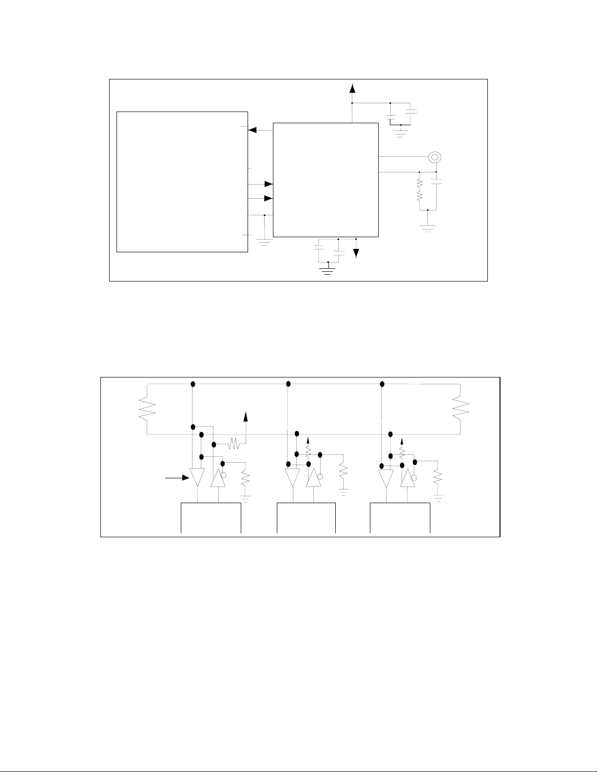
Figure 6 illustrates the COM20051I interface to the transmission media used to connect the node to the network.
Table 2 lists different types of cable which are suitable for ARCNET applications.1 The user may interface to the
cable of choice in one of three ways:
1
Please refer to TN7-5 -
distance, termi nat i on, and node count for ARCNET nodes.
Traditional Hybrid Interface
The Traditional Hybrid Interface is that which is used with previous ARCNET devices. The Hybrid Interface is
recommended if the node is to be placed in a network with other Hybrid-Interfaced nodes. The Traditional Hybrid
Interface is for use with nodes operating at 2.5 Mbps only. The transformer coupling of the Hybrid offers isolation for
the safety of the system and offers high Common Mode Rejection. The Traditional Hybrid Interface uses circuits like
SMSC's HYC9068 or HYC9088 to transfer the pulse-encoded data between the cable and the COM20051I. The
COM20051I transmits a logic "1" by generating two 100nS non-overlapping negative pulses, nPULSE1 and
nPULSE2. Lack of pulses indicates a logic "0". The nPULSE1 and nPULSE2 signals are sent to the Hybrid, which
creates a 200nS dipulse signal on the
coupled through the transformer of the LAN Driver, which produces a positive pulse at the RXIN pin of the
COM20051I. The pulse on the RXIN pin represents a logic "1". Lack of pulse represents a logic "0". Typically, RXIN
pulses occur at multiples of 400nS. The COM20051I can tolerate distortion (bit jitter) of plus or minus 100nS and still
correctly capture and convert the RXIN pulses to NRZ format. Figure 8 illustrates the events which occur in
transmission or reception of data consisting of 1, 1, 0.
Backplane Configuration
The Backplane Configuration is recommended for cost-sensitive, short-distance applications like backplanes and
instrumentation. This mode is advantageous because it saves components, cost, and power.
Cabling Guidelines for the COM20020 ULANC
The internal RAM is accessed via a
Note that at 5 Mbps data rate, the internal arbiter must be
The pointer may be used in the auto-increment mode
medium.
During reception, the 200nS dipulse appearing on the media is
, available from SMSC, for recommended cabling
SMSC DS – COM20051I Page 18 Rev. 03/27/2000
RXIN
HYC9068 or
HYC9088
RXIN
+5V
6
10
uF
+
0.47
uF
COM20051I
nTXEN
nPULSE1
nPULSE2
GND
N/C
nPULSE1
nPULSE2
17, 19,
4, 13, 14
0.47
uF
12
11
3
+
10
uF
-5V
5.6K
1/2W
5.6K
1/2W
Traditional Hybrid
Configuration
0.01 uF
1KV
FIGURE 6 – DIPULSE HYBRID CONFIGURATION
RT
+VCC
RBIAS
75176B or
Equiv.
RBIAS
RT
+VCC
RBIAS
+VCC
COM20051I
COM20051I
COM20051I
FIGURE 7 – COM20051I NETWORK USING RS-485 DIFFERENTIAL TRANSCEIVERS
SMSC DS – COM20051I Page 19 Rev. 03/27/2000
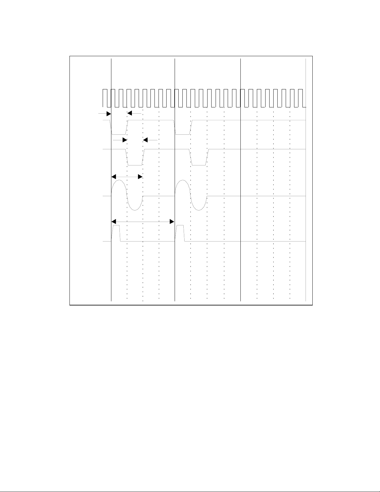
(
)
10
20M HZ
CLOCK
FOR
REF.
ONLY
100ns
nPULSE1
1
100ns
nPU LSE2
200ns
DIPULSE
400ns
RXIN
FIGURE 8 – DIPULSE WAVEFORM FOR BIT DATA OF 1-1-0
SMSC DS – COM20051I Page 20 Rev. 03/27/2000

Since the Backplane Configuration encodes data differently than the traditional Hybrid Configuration, nodes utilizing
the Backplane Configuration cannot communicate directly with nodes utilizing the Traditional Hybrid Configuration.
The Backplane Configuration does not isolate the node from the media nor protect it from Common Mode noise, but
Common Mode Noise is less of a problem in short distances.
The COM20051I supplies a programmable output driver for Backplane Mode operation. A push/pull or open drain
driver can be selected by programming the P1MODE bit of the Setup Register (see register descriptions for details.)
The COM20051I defaults to an open drain output.
The Backplane Configuration provides for direct connection between the COM20051I and the
open drain configuration of the output driver.
Only one pull-up resistor (for open drain only) is required somewhere
physical medium in
on the media (not on each individual node). The nPULSE1 signal, in this mode, is an open drain or push/pull driver
and is used to directly drive the media. It issues a 200nS negative pulse to transmit a logic "1". Note that when used
in the open-drain mode, the COM20051I does not have a fail/safe input on the RXIN pin.
The nPULSE1 signal actually contains a weak pull-up resistor. This pull-up should not take the place of the resistor
required on the media for open drain mode. In typical applications, the serial backplane is terminated at both ends
and a bias is provided by the external pull-up resistor.
The RXIN signal is directly connected to the cable via an internal Schmitt trigger. A negative pulse on this input
indicates a logic "1". Lack of pulse indicates a logic "0". For typical single-ended backplane applications, RXIN is
connected to nPULSE1 to make the serial backplane data line. A ground line (from the coax or twisted pair) should
run in parallel with the signal. For applications requiring different treatment of the receive signal (like filtering or
squelching), nPULSE1 and RXIN remain as independent pins. External differential drivers/receivers for increased
range and common mode noise rejection, for example, would require the signals to be independent of one another.
When the device is in Backplane Mode, the clock provided by the nPULSE2 signal may be used for encoding the
data into a different encoding scheme or other synchronous operations needed on the serial data stream.
Differential Driver Configuration
The Differential Driver Configuration is a special case of the Backplane Mode. It is a DC coupled configuration
recommended for applications like car-area networks (CAN) or other cost-sensitive applications which do not require
direct compatibility with existing ARCNET nodes and do not require isolation.
Figure 7 illustrates this configuration.
The Differential Driver Configuration cannot communicate directly with nodes utilizing the Traditional Hybrid
Configuration. Like the Backplane Configuration, the Differential Driver Configuration does not isolate the node from
physical medium.
the
The Differential Driver interface includes a RS485 Driver/Receiver to transfer the data between the cable and the
COM20051I. The nPULSE1 signal transmits the data, provided the nTXEN signal is active. The nPULSE1 signal
issues a 200nS negative pulse to transmit a logic "1". The RXIN pin receives the data. A negative pulse on this
input indicates a logic "1". Lack of pulse indicates a logic "0". The transmitter portion of the COM20051I is disabled
during reset and the nPULSE1, nPULSE2 and nTXEN pins are inactive.
CABLE TYPE
Table 2 - Typical Media
NOMINAL
IMPEDANCE
ATTENUATION PER 1000 FT.
AT 5MHZ
RG-62 Belden #86262 93 5.5dB
RG-59/U Belden #89108 75 7.0dB
RG-11/U Belden #89108 75 5.5dB
IBM Type 1* Belden #89688 150 7.0dB
IBM Type 3* Telephone Twisted Pair Belden #1155A 100 17.9dB
COMCODE 26 AWG Twisted Pair Part #105-064-703 105 16.0dB
*Non-plenum-rated cables of this type are also available.
Note:
For more detailed information on Cabling options including RS-485, transformer-coupled RS-485 and Fiber
Optic interfaces, please refer to TN7-5 -
Cabling Guidelines for the COM20020 ULANC
available from Standard
,
Microsystems Corporation.
SMSC DS – COM20051I Page 21 Rev. 03/27/2000
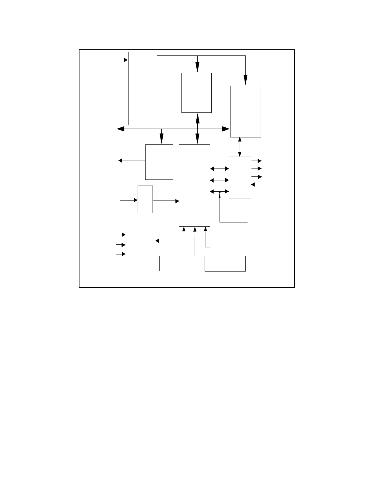
ALE
AD0-AD7
nINTR
nRESET IN
nRD
nW R
nCS
ADDRESS
DECODING
CIRCUITRY
1K x 8
RAM
ADDITIONAL
REGISTERS
STATUS/
COMMAND
REGISTER
MICRO-
SEQUENCER
AND
TX/RX
LOG IC
WORKING
RESET
REGISTERS
LOG IC
BUS
ARBITRATION
CIRCUITRY
FIGURE 9 – ARCNET CORE BLOCK DIAGRAM
RECONFIGURATION
TIMER
NODE ID
LOG IC
nPULSE1
nPULSE2
nTXEN
RXIN
20 MH z
or 40 MHz
CORE CLOCK
SMSC DS – COM20051I Page 22 Rev. 03/27/2000

ARCNET CORE FUNCTIONAL DESCRIPTION
MICROSEQUENCER
The ARCNET core contains an internal microsequencer which performs all of the control operations necessary to
carry out the ARCNET protocol. It consists of a clock generator, a 544 x 8 ROM, a program counter, two instruction
registers, an instruction decoder, a no-op generator, jump logic, and reconfiguration logic.
The ARCNET core derives The Program Counter Clock and Instruction Ex ecution Clock from the SYSTEM CLOCK.
If the system clock is 40 MHz the Program Counter Clock runs at 10 MHz and the Instruction Execution Clock runs at
5 MHz. If the System Clock is 20 MHz the above clocks run at 5 MHz and 2.5 MHz respectively.
is stored in the ROM and the instructions are fetched and then placed into the instruction registers. One register
holds the op code, while the other holds the immediate data. Once the instruction is fetched, it is decoded by the
internal instruction decoder, at which point the ARCNET core proceeds to execute the instruction. When a no-op
instruction is encountered, the microsequencer enters a timed loop and the program counter is temporarily stopped
until the loop is complete. When a jump instruction is encountered, the program counter is loaded with the jump
address from the ROM. The ARCNET core contains an internal reconfiguration timer which interrupts the
microsequencer if it has timed out. At this point the program counter is cleared and the MYRECON bit of the
Diagnostic Status Register is set.
INTERNAL REGISTERS
The ARCNET core contains eight internal registers. Tables 4 and 5 illustrate the ARCNET core register map.
Reserved locations should not be accessed. All undefined bits are read as undefined and must be written as logic
"0".
Interrupt Mask Register (IMR)
The ARCNET core is capable of generating an interrupt signal when certain status bits become true. A write to the
IMR specifies which status bits will be enabled to generate an interrupt. The bit positions in the IMR are in the same
position as their corresponding status bits in the Status Register and Diagnostic Status Register. A logic "1" in a
particular position enables the corresponding interrupt. The Status bits capable of generating an interrupt include the
Receiver Inhibited bit, New Next ID bit, Excessive NAK bit, Reconfiguration Timer bit, and Transmitter Available bit.
No other Status or Diagnostic Status bits can generate an interrupt.
The five maskable status bits are ANDed with their respective mask bits, and the results are ORed to produce the
interrupt signal. An RI or TA interrupt is masked when the corresponding mask bit is reset to logic "0", but will
reappear when the corresponding mask bit is set to logic "1" again, unless the interrupt status condition has been
cleared by this time. A RECON interrupt is cleared when the "Clear Flags" command is issued. An EXCNAK
interrupt is cleared when the "POR Clear Flags" command is issued. A New Next ID interrupt is cleared by reading
the New Next ID Register. The Interrupt Mask Register defaults to the value 0000 0000 upon hardware reset only.
Refer to Table 3.
(Location +00Hex)
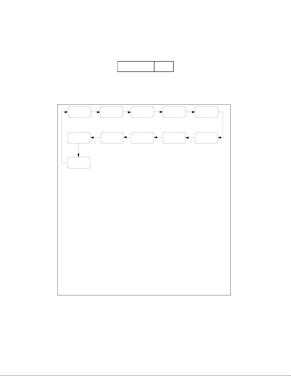
Table 3 - Cleaning Interrupt Bit
INTERRUPT TYPE CLEANING INTERRUPT BIT
RI Issue "Enable Receive to Page Fnn" command
EXCNAK Issue "Clean Flags" Command with "p" bit set
RECON Issue "Clear Flags" Command with "r" bit set
New Next ID Read New Next ID Register
TA Issue "Enable Transmit From Page Fnn"
Command
The microprogram
SMSC DS – COM20051I Page 23 Rev. 03/27/2000
 Loading...