

Standard Microsystems Corporation COM20020P, COM20020LJP, COM20020IP, COM20020ILJP Datasheet

COM20020D
COM20020 ULANC
Revision D
Universal Local Area Network Controller
with 2K x 8 On-Board RAM
FEATURES
• New Features for Rev. D
- Data Rates up to 5 Mbps
- Programmable Reconfiguration Times
• 24 Pin DIP, 28 Pin PLCC Package
• Ideal for Industrial/Factory/Building
Automation and Transportation
Applications
• Deterministic, (ANSI 878.1), Token Passing
ARCNET Protocol
• Minimal Microcontroller and Media
Interface Logic Required
• Flexible Interface For Use With All
Microcontrollers or Microprocessors
• Automatically Detects Type of
Microcontroller Interface
• 2Kx8 On-Chip Dual Port RAM
• Command Chaining for Packet Queuing
• Sequential Access to Internal RAM
• Software Programmable Node ID
• Eight, 256 Byte Pages Allow Four Pages TX
and RX Plus Scratch-Pad Memory
• Next ID Readable
• Internal Clock Scaler and Clock Multiplier for
Adjusting Network Speed
• Operating Temperature Range of -40oC to
+85oC
• Self-Reconfiguration Protocol
• Supports up to 255 Nodes
• Supports Various Network Topologies (Star,
Tree, Bus...)
• CMOS, Single +5V Supply
• Duplicate Node ID Detection
• Powerful Diagnostics
• Receive All Packets Mode
• Flexible Media Interface:
- Traditional Hybrid Interface For Long
Distances up to Four Miles at 2.5Mbps.
- RS485 Differential Driver Interface For
Low Cost, Low Power, High Reliability
GENERAL DESCRIPTION
SMSC's COM20020D is a member of the family of
Embedded ARCNET Controllers from Standard
Microsystems Corporation. The device is a
general purpose communications controller for
networking microcontrollers and intelligent
peripherals in industrial, automotive, and
embedded control environments using an
ARCNET® protocol engine. The small 24 pin
package, flexible microcontroller and media
interfaces, eight- page message support, and
extended temperature range of the COM20020D
make it the only true network controller optimized
for use in industrial, embedded, and automotive
applications. Using an ARCNET protocol engine
is the ideal solution for embedded control
applications because it provides a deterministic

2
token-passing protocol, a highly reliable and
proven networking scheme, and a data rate of up
to 5 Mbps when using the COM20020D.
A token-passing protocol provides predictable
response times because each network event
occurs within a predetermined time interval, based
upon the number of nodes on the network. The
deterministic nature of ARCNET is essential in
real time applications. The integration of the 2Kx8
RAM buffer on-chip, the Command Chaining
feature, the 5 Mbps maximum data rate, and the
internal diagnostics make the COM20020D the
highest performance embedded communications
device available. With only one COM20020D and
one microcontroller, a complete communications
node may be implemented.
ARCNET is a registered trademark of Datapoint Corporation

3
TABLE OF CONTENTS
FEATURES....................................................................................................................................... 1
GENERAL DESCRIPTION ................................................................................................................ 1
PIN CONFIGURATION...................................................................................................................... 4
DESCRIPTION OF PIN FUNCTIONS.................................................................................................5
PROTOCOL DESCRIPTION .............................................................................................................. 8
NETWORK PROTOCOL ............................................................................................................... 8
DATA RATES ............................................................................................................................... 8
NETWORK RECONFIGURATION................................................................................................. 9
BROADCAST MESSAGES.......................................................................................................... 10
EXTENDED TIMEOUT FUNCTION ............................................................................................. 10
LINE PROTOCOL....................................................................................................................... 10
SYSTEM DESCRIPTION................................................................................................................. 13
MICROCONTROLLER INTERFACE............................................................................................13
TRANSMISSION MEDIA INTERFACE.........................................................................................17
FUNCTIONAL DESCRIPTION......................................................................................................... 22
MICROSEQUENCER..................................................................................................................22
INTERNAL REGISTERS ............................................................................................................. 25
INTERNAL RAM ......................................................................................................................... 38
COMMAND CHAINING............................................................................................................... 43
INITIALIZATION SEQUENCE...................................................................................................... 45
IMPROVED DIAGNOSTICS........................................................................................................ 46
OPERATIONAL DESCRIPTION ...................................................................................................... 49
MAXIMUM GUARANTEED RATINGS*........................................................................................ 49
DC ELECTRICAL CHARACTERISTICS ....................................................................................... 49
TIMING DIAGRAMS........................................................................................................................ 52
APPENDIX A................................................................................................................................... 67
APPENDIX B: EXAMPLE OF INTERFACE CIRCUIT DIAGRAM TO ISA BUS ................................ 71
APPENDIX C................................................................................................................................... 72
SOFTWARE IDENTIFICATION OF THE COM20020 REV B, REV C AND REV D ............................ 72
For more details on the ARCNET protocol engine and traditional dipulse signaling schemes,
please refer to the ARCNET Local Area Network Standard, available from Standard Microsystems
Corporation or the ARCNET Designer's Handbook, available from Datapoint Corporation.
For more detailed information on cabling options including RS485, transformer-coupled RS-485
and Fiber Optic interfaces, please refer to the following technical note which is available from
Standard Microsystems Corporation: Technical Note 7-5 - Cabling Guidelines for the COM20020
ULANC.
4
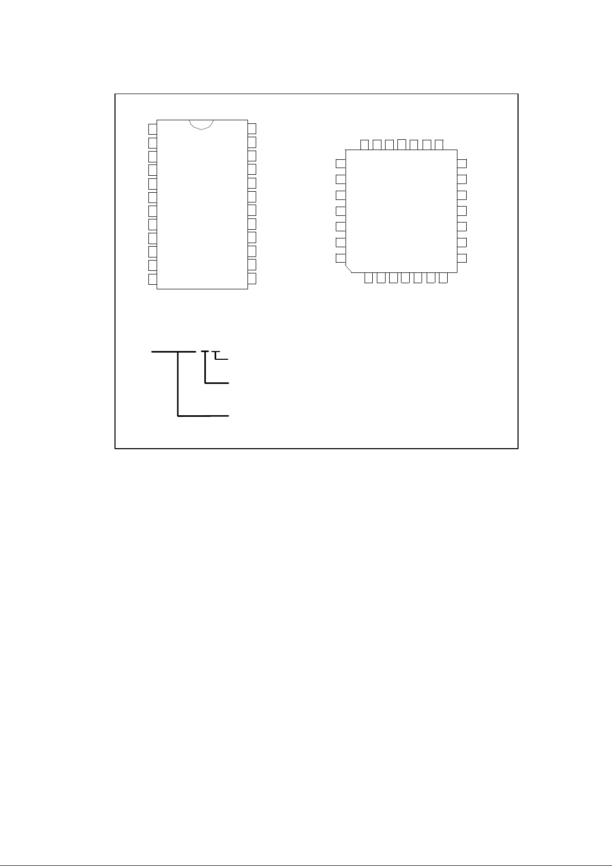
PIN CONFIGURATION
24
23
22
21
20
19
18
17
16
15
14
13
1
2
3
4
5
6
7
8
9
10
11
12
A0/nMUX
A1
A2/ALE
AD0
AD1
AD2
D3
D4
D5
D6
D7
nRD/nDS
nWR/DIR
nCS
nINTR
nRESET IN
nTXEN
RXIN
nPULSE2
nPULSE1
XTAL2
XTAL1
VDD
26
27
28
1
2
3
4
18
17
16
15
14
13
12
25 24 23 22 21 20 19
5 6 7 8 9 10 11
n
C
S
n
I
N
T
R
n
R
E
S
E
T
I
N
V
S
S
n
T
X
E
N
R
X
I
N
n
P
U
L
S
E
2
A
D
1
V
S
S
A
D
2
D3D4D5D
6
nPULSE 1
XTAL2
XTAL1
VDD
VSS
N/C
D7
nWR/DIR
nRD/nDS
VDD
A2/ALE
AD0
A1
Packages: 24-Pin DIP or 28-Pin PLCC
Ordering Information:
COM20020
VSS
A0/nMUX
PACKAGE TYPE: P = Plastic, LJP = PLCC
TEMP RANGE: (Blank) = Commercial: 0°C to +70°C
I = Industrial: -40°C to +85°C
DEVICE TYPE: 20020 = Universal Local Area Network Controller
(with 2K x 8 RAM)
P
I

5
DESCRIPTION OF PIN FUNCTIONS
DIP PIN
NO.
PLCC PIN
NO. NAME SYMBOL DESCRIPTION
MICROCONTROLLER INTERFACE
1-3 1-3 Address
0-2
A0/nMUX,
A1,A2/ALE
Input. On a non-multiplexed mode, A0-A2
are address input bits. (A0 is the LSB) On a
multiplexed address/data bus, nMUX tied
Low, A1 is left open, and ALE is tied to the
Address Latch Enable signal. A1 is
connected to an internal pull-up resistor.
4-11 4-6,8-12 Data 0-7 AD0-AD2,
D3-D7
Input/Output. On a non-multiplexed bus,
these signals are used as the data lines for
the device. On a multiplexed address/data
bus, AD0-AD2 act as the address lines
(latched by ALE) and as the low data lines for
the device. D3-D7 are always used for data
only. These signals are connected to internal
pull-up resistors.
23 27 nRead/nData
Strobe
nRD/nDS Input. On a 68XX-like bus, nDS is an active
low signal issued by the microcontroller as the
data strobe signal to strobe the data onto the
bus. On a 80XX-like bus, nRD is an active
low signal issued by the microcontroller to
indicate a read operation.
22 26 nWrite/
Direction
nWR/DIR
Input. On a 68XX-like bus, DIR is issued by
the microcontroller as the Read/nWrite signal
to determine the direction of data transfer. In
this case, a logic "1" selects a read operation,
while a logic "0" selects a write operation. In
this case, data is actually strobed by the nDS
signal. On an 80XX-like bus, nWR is an
active low signal issued by the microcontroller
to indicate a write operation. In this case, a
logic "0" on this pin, when the COM20020D is
accessed, enables data from the data bus to
be written to the device.
19 23 nReset in nRESET
Input. This active low signal executes a
hardware reset.
20 24 nInterrupt nINTR
Output. This active low signal is generated by
the COM20020D when an enabled interrupt
condition occurs.
21 25 nChip Select nCS Input. This active low signal selects the
COM20020D for an access.

6
DIP PIN
NO.
PLCC PIN
NO. NAME SYMBOL DESCRIPTION
TRANSMISSION MEDIA INTERFACE
16,15 19,18
nPulse 2,
nPulse 1
nPULSE2,
nPULSE1
Output (nPULSE1), Input/Output (nPULSE2).
In Normal Mode, these active low signals
carry the transmit data information, encoded
in pulse format, as DIPULSE waveform.
When the device is in Backplane Mode, the
nPULSE1 signal driver is programmable
(push/pull or open-drain), while the nPULSE2
signal provides a clock with frequency of
double the data rate. nPULSE1 is connected
to a weak internal pull-up resistor on the
open/drain driver in backplane mode.
17 20 Receive In RXIN Input. This signal carries the receive data
information from the line tranceiver.
18 21
nTransmit
nEnable
nTXEN
Output. This signal is used prior to the Power-
up to enable the line drivers for transmission.
The polarity of the signal is programmable
through the nPULSE2 pin.
nPULSE2 floating before Power-up: nTXEN
active low (Default option)
nPULSE2 grounded before Power-up:
nTXEN active high (This option is only
available in Backplane Mode)
13,14 16,17 Crystal
Oscillator
XTAL1,
XTAL2
An external crystal should be connected to
these pins. Oscillation frequency range is
from 10 to 20 MHz. If an external TTL clock is
used instead, it must be connected to XTAL1
with a 390Ω pull-up resistor, and XTAL2
should be left floating.
24 15,28 Power
Supply
V
DD
+5 Volt Power Supply pin.
12 7,14,22 Ground V
SS
Ground pin.
7
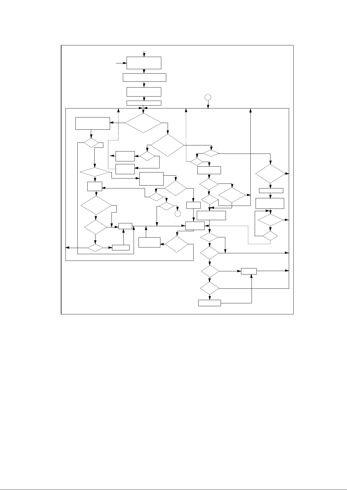
FIGURE 1 - COM20020 OPERATION
Invitation
to Transmit to
this ID?
Y
N
Free Buffer
Enquiry to
this ID?
SOH?
Y N
Y N
RI?
Write SID
to Buffer
DID
=0?
DID
=ID?
Write Buffer
with Packet
CRC
OK?
LENGTH
OK?
DID
=0?
DID
=ID?
SEND ACK
N
Y
N
Y
N
Y
N
Broadcast
Enabled?
N
Y
N
No Activity
for 41
uS?
Y
N
Set NID=ID
Start Timer:
T=(255-ID)
Activity
On Line?
Y
N
T=0?
Set RI
RI?
Transmit
NAK
Transmit
ACK
Set NID=ID
Write ID to
RAM Buffer
Send
Reconfigure
Burst
Power On
Reconfigure
Timer has
Timed Out
Start
Reconfiguration
Timer (420 mS)*
TA?
Broadcast?
Transmit
Free Buffer
Enquiry
No
Activity
Pass the
Token
Set TA
Y
N
ACK?
NAK?
1
No
Activity
NY
Increment
NID
Send
Packet
Was Packet
Broadcast?
No
Activity
N
ACK? Set TMA
Set TA
x 73 us
for 37.4
us?
for 37.4
us?
for 37.4
us?
YN
N
Y
Y N
NY
N
N
N
N
1
Y
Y
Y
Y
Y
Y
Y
N
Y
Read Node ID
ID refers to the identification number of the ID assigned to this node.
NID refers to the next identification number that receives the token
after this ID passes it.
-
-
-
-
SID refers to the source identification.
DID refers to the destination identification.
SOH refers to the start of header character; preceeds all data packets.
-
Y N
* Reconfig timer is programmable via setup2 register bits 1, 0.
Note - All time values are valid for 5 Mbps.

8
PROTOCOL DESCRIPTION
NETWORK PROTOCOL
Communication on the network is based on a
token passing protocol. Establishment of the
network configuration and management of the
network protocol are handled entirely by the
COM20020D's internal microcoded sequencer. A
processor or intelligent peripheral transmits data
by simply loading a data packet and its destination
ID into the COM20020D's internal RAM buffer,
and issuing a command to enable the transmitter.
When the COM20020D next receives the token, it
verifies that the receiving node is ready by first
transmitting a FREE BUFFER ENQUIRY
message. If the receiving node transmits an
ACKnowledge message, the data packet is
transmitted followed by a 16-bit CRC. If the
receiving node cannot accept the packet (typically
its receiver is inhibited), it transmits a Negative
AcKnowledge message and the transmitter
passes the token. Once it has been established
that the receiving node can accept the packet and
transmission is complete, the receiving node
verifies the packet. If the packet is received
successfully, the receiving node transmits an
ACKnowledge message (or nothing if it is not
received successfully) allowing the transmitter to
set the appropriate status bits to indicate
successful or unsuccessful delivery of the packet.
An interrupt mask permits the COM20020D to
generate an interrupt to the processor when
selected status bits become true. Figure 1 is a
flow chart illustrating the internal operation of the
COM20020D connected to a 20 MHz crystal
oscillator.
DATA RATES
The COM20020D is capable of supporting data
rates from 156.25 Kbps to 5 Mbps. The following
protocol description assumes a 5 Mbps data rate.
To attain the faster data rates, the clock frequency
may be doubled by the internal clock multiplier
(see next section). For slower data rates, an
internal clock divider scales down the clock
frequency. Thus all timeout values are scaled as
shown in the following table:
Example: IDLE LINE Timeout @ 5 Mbps = 41 µs.
IDLE LINE Timeout for 156.2 Kbps is 41 µs * 32 =
1.3 ms
INTERNAL
CLOCK
FREQUENCY
CLOCK
PRESCALER DATA RATE
TIMEOUT SCALING
FACTOR (MULTIPLY BY)
40 MHz Div. by 8 5 Mbps 1
20 MHz Div. by 8
Div. by 16
Div. by 32
Div. by 64
Div. by 128
2.5 Mbps
1.25 Mbps
625 Kbps
312.5 Kbps
156.25 Kbps
2
4
8
16
32

9
Selecting Clock Frequencies Above 2.5 Mbps
To realize a 5 Mbps network, an external 40 MHz
clock must be input. However, since 40 MHz is
near the frequency of FM radio band, it is not
practical for use for noise emission reasons.
Therefore, higher frequency clocks are
generated from the 20 MHz crystal as selected
through two bits in the Setup2 register,
CKUP[1,0] as shown below. The selected clock
is supplied to the ARCNET controller.
CKUP1 CKUP0 CLOCK FREQUENCY (DATA RATE)
0 0 20 MHz (Up to 2.5Mbps) Default (Bypass)
0 1 40 MHz (Up to 5Mbps)
1 0 Reserved
1 1 Reserved
This clock multiplier is powered-down (bypassed)
on default. After changing the CKUP1 and
CKUP0 bits, the ARCNET core operation is
stopped and the internal PLL in the clock
generator is awakened and it starts to generate
the 40 MHz. The lock out time of the internal PLL
is 8uSec typically. After more than 8 µsec (this
wait time is defined as 1 msec in this data sheet),
it is necessary to write command data '18H' to
the command register to re-start the ARCNET
core operation. This clock generator is called
“clock multiplier”.
Changing the CKUP1 and CKUP0 bits must be
one time or less after releasing hardware reset.
The EF bit in the SETUP2 register must be set
when the data rate is over 5 Mbps.
NETWORK RECONFIGURATION
A significant advantage of the COM20020D is its
ability to adapt to changes on the network.
Whenever a new node is activated or deactivated,
a NETWORK RECONFIGURATION is performed.
When a new COM20020D is turned on (creating
a new active node on the network), or if the
COM20020D has not received an INVITATION
TO TRANSMIT for 420mS, or if a software reset
occurs, the COM20020D causes a NETWORK
RECONFIGURATION by sending a
RECONFIGURE BURST consisting of eight
marks and one space repeated 765 times. The
purpose of this burst is to terminate all activity on
the network. Since this burst is longer than any
other type of transmission, the burst will interfere
with the next INVITATION TO TRANSMIT,
destroy the token and keep any other node from
assuming control of the line.
When any COM20020D senses an idle line for
greater than 41µS, which occurs only when the
token Is lost, each COM20020D starts an internal
timeout equal to 73µs times the quantity 255
minus its own ID. The COM20020D starts network
reconfiguration by sending an invitation to transmit
first to itself and then to all other nodes by
decrementing the destination Node ID. If the
timeout expires with no line activity, the
COM20020D starts sending INVITATION TO
TRANSMIT with the Destination ID (DID) equal to
the currently stored NID. Within a given network,
only one COM20020D will timeout (the one with
the highest ID number). After sending the
INVITATION TO TRANSMIT, the COM20020D
waits for activity on the line. If there is no activity
for 37.4µS, the COM20020D increments the NID
value and transmits another INVITATION TO
TRANSMIT using the NID equal to the DID. If
activity appears before the 37.4µS timeout
expires, the COM20020D releases control of the
line. During NETWORK RECONFIGURATION,
INVITATIONS TO TRANSMIT are sent to all NIDs
(1-255).
Each COM20020D on the network will finally have
saved a NID value equal to the ID of the
COM20020D that it released control to. At this
point, control is passed directly from one node to
the next with no wasted INVITATIONS TO
TRANSMIT being sent to ID's not on the network,
until the next NETWORK RECONFIGURATION
occurs. When a node is powered off, the previous
node attempts to pass the token to it by issuing an

10
INVITATION TO TRANSMIT. Since this node
does not respond, the previous node times out
and transmits another INVITATION TO
TRANSMIT to an incremented ID and eventually a
response will be received.
The NETWORK RECONFIGURATION time
depends on the number of nodes in the network,
the propagation delay between nodes, and the
highest ID number on the network, but is typically
within the range of 12 to 30.5 mS.
BROADCAST MESSAGES
Broadcasting gives a particular node the ability to
transmit a data packet to all nodes on the network
simultaneously. ID zero is reserved for this
feature and no node on the network can be
assigned ID zero. To broadcast a message, the
transmitting node's processor simply loads the
RAM buffer with the data packet and sets the DID
equal to zero. Figure 4 illustrates the position of
each byte in the packet with the DID residing at
address 0X01 or 1 Hex of the current page
selected in the "Enable Transmit from Page fnn"
command. Each individual node has the ability to
ignore broadcast messages by setting the most
significant bit of the "Enable Receive to Page fnn"
command to a logic "0".
EXTENDED TIMEOUT FUNCTION
There are three timeouts associated with the
COM20020D operation. The values of these
timeouts are controlled by bits 3 and 4 of the
Configuration Register and bit 5 of the Setup 1
Register.
Response Time
The Response Time determines the maximum
propagation delay allowed between any two
nodes, and should be chosen to be larger than
the round trip propagation delay between the two
furthest nodes on the network plus the maximum
turn around time (the time it takes a particular
COM20020D to start sending a message in
response to a received message) which is
approximately 6.4 µS. The round trip propagation
delay is a function of the transmission media and
network topology. For a typical system using
RG62 coax in a baseband system, a one way
cable propagation delay of 15.5 µS translates to a
distance of about 2 miles. The flow chart in Figure
1 uses a value of 37.4 µS (15.5 + 15.5 + 6.4) to
determine if any node will respond.
Idle Time
The Idle Time is associated with a NETWORK
RECONFIGURATION. Figure 1 illustrates that
during a NETWORK RECONFIGURATION one
node will continually transmit INVITATIONS TO
TRANSMIT until it encounters an active node. All
other nodes on the network must distinguish
between this operation and an entirely idle line.
During NETWORK RECONFIGURATION, activity
will appear on the line every 41 µS. This 41 µS is
equal to the Response Time of 37.4 µS plus the
time it takes the COM20020D to start
retransmitting another message (usually another
INVITATION TO TRANSMIT).
Reconfiguration Time
If any node does not receive the token within the
Reconfiguration Time, the node will initiate a
NETWORK RECONFIGURATION. The ET2 and
ET1 bits of the Configuration Register allow the
network to operate over longer distances than the
2 miles stated earlier. The logic levels on these
bits control the maximum distances over which the
COM20020D can operate by controlling the three
timeout values described above. For proper
network operation, all COM20020D's connected to
the same network must have the same Response
Time, Idle Time, and Reconfiguration Time.
LINE PROTOCOL
The ARCNET line protocol is considered
isochronous because each byte is preceded by a
start interval and ended with a stop interval. Unlike
asynchronous protocols, there is a constant
amount of time separating each data byte. On a 5
Mbps network, each byte takes exactly 11 clock
intervals of 200ns each. As a result, one byte is
transmitted every 2.2 µS and the time to transmit
a message can be precisely determined. The line
idles in a spacing (logic "0") condition. A logic "0"

11
is defined as no line activity and a logic "1" is
defined as a negative pulse of 100nS duration. A
transmission starts with an ALERT BURST
consisting of 6 unit intervals of mark (logic "1").
Eight bit data characters are then sent, with each
character preceded by 2 unit intervals of mark and
one unit interval of space. Five types of
transmission can be performed as described
below:
Invitations To Transmit
An Invitation To Transmit is used to pass the
token from one node to another and is sent by the
following sequence:
• An ALERT BURST
• An EOT (End Of Transmission: ASCII code
04H)
• Two (repeated) DID (Destination ID)
characters
ALERT
BURST
EOT DID DID
Free Buffer Enquiries
A Free Buffer Enquiry is used to ask another node
if it is able to accept a packet of data. It is sent by
the following sequence:
• An ALERT BURST
• An ENQ (ENQuiry: ASCII code 85H)
• Two (repeated) DID (Destination ID)
characters
ALERT
BURST
ENQ DID DID
Data Packets
A Data Packet consists of the actual data being
sent to another node. It is sent by the following
sequence:
• An ALERT BURST
• An SOH (Start Of Header--ASCII code 01H)
• An SID (Source ID) character
• Two (repeated) DID (Destination ID)
characters
• A single COUNT character which is the 2's
complement of the number of data bytes to
follow if a short packet is sent, or 00H
followed by a COUNT character if a long
packet is sent.
• N data bytes where COUNT = 256-N (or 512N for a long packet)
• Two CRC (Cyclic Redundancy Check)
characters. The CRC polynomial used is:
X16 + X15 + X2 + 1.
ALERT
BURST
SOH
SID
DID
DID
COUNT
data
data
CRC
CRC

12
Acknowledgements
An Acknowledgement is used to acknowledge
reception of a packet or as an affirmative
response to FREE BUFFER ENQUIRIES and is
sent by the following sequence:
• An ALERT BURST
• An ACK (ACKnowledgement--ASCII code
86H) character
ALERT BURST ACK
Negative Acknowledgements
A Negative Acknowledgement is used as a
negative response to FREE BUFFER
ENQUIRIES and is sent by the following
sequence:
• An ALERT BURST
• A NAK (Negative Acknowledgement--ASCII
code 15H) character
ALERT BURST NAK

13
SYSTEM DESCRIPTION
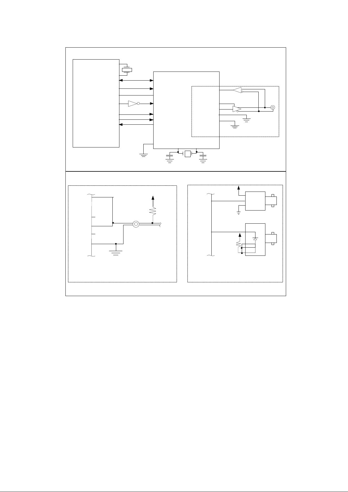
MICROCONTROLLER INTERFACE
The top halves of Figures 2 and 3 illustrate typical
COM20020D interfaces to the microcontrollers.
The interfaces consist of a 8-bit data bus, an
address bus and a control bus. In order to support
a wide range of microcontrollers without requiring
glue logic and without increasing the number of
pins, the COM20020D automatically detects and
adapts to the type of microcontroller being used.
Upon hardware reset, the COM20020D first
determines whether the read and write control
signals are separate READ and WRITE signals
(like the 80XX) or DIRECTION and DATA
STROBE (like the 68XX). To determine the type of
control signals, the device requires the software to
execute at least one write access to external
memory before attempting to access the
COM20020D. The device defaults to 80XX-like
signals. Once the type of control signals are
determined, the COM20020D remains in this
interface mode until the next hardware reset
occurs. The second determination the
COM20020D makes is whether the bus is
multiplexed or non-multiplexed. To determine the
type of bus, the device requires the software to
write to an odd memory location followed by a
read from an odd location before attempting to
access the COM20020D. The signal on the A0 pin
during the odd location access tells the
COM20020D the type of bus. Since multiplexed
operation requires A0 to be active low, activity on
the A0 line tells the COM20020D that the bus is
non-multiplexed. The device defaults to
multiplexed operation. Both determinations may
be made simultaneously by performing a WRITE
followed by a READ operation to an odd location
within the COM20020D Address space 20020D
registers. Once the type of bus is determined, the
COM20020D remains in this interface mode until
hardware reset occurs.
Whenever nCS and nRD are activated, the preset
determinations are assumed as final and will not
be changed until hardware reset. Refer to
Description of Pin Functions section for details on
the related signals. All accesses to the internal
RAM and the internal registers are controlled by
the COM20020D. The internal RAM is accessed
via a pointer-based scheme (refer to the
Sequential Access Memory section), and the
internal registers are accessed via direct
addressing. Many peripherals are not fast enough
to take advantage of high-speed microcontrollers.
Since microcontrollers do not typically have
READY inputs, standard peripherals cannot
extend cycles to extend the access time. The
access time of the COM20020D, on the other
hand, is so fast that it does not need to limit the
speed of the microcontroller. The COM20020D is
designed to be flexible so that it is independent of
the microcontroller speed.
The COM20020D provides for no wait state
arbitration via direct addressing to its internal
registers and a pointer based addressing scheme
to access its internal RAM. The pointer may be
used in auto-increment mode for typical
sequential buffer emptying or loading, or it can be
taken out of auto-increment mode to perform
random accesses to the RAM. The data within
the RAM is accessed through the data register.
Data being read is prefetched from memory and
placed into the data register for the microcontroller
to read. It is important to notice that only by
writing a new address pointer (writing to an
address pointer low), one obtains the contents of
COM20020D internal RAM. Performing only read
from the Data Register does not load new data
from the internal RAM. During a write operation,
the data is stored in the data register and then
written into memory. Whenever the pointer is
loaded for reads with a new value, data is
immediately prefetched to prepare for the first
read operation.
14
FIGURE 2 - MULTIPLEXED, 8051-LIKE BUS INTERFACE WITH RS-485 INTERFACE
RXIN
nPULSE1
nPULSE2
TXEN
GND
+5V
100 Ohm
BACKPLANE CONFIGURATION
FIGURE A
RXIN
nPULSE1
FIGURE B
Receiver
HFD3212-002
2
+5V
7
6
Transmitter
HFE4211-014
+5V
3
2 Fiber Interface
(ST Connectors)
2
6
7
NOTE: COM20020 must be in backplane mode
AD0-AD7
nINT1
RESET
nRD
nWR
A15
AD0-AD2, D3-D7
nCS
nRESET
nRD/nDS
nWR/DIR
nINTR
A2/BALE
ALE
XTAL1
XTAL2
GND
RXIN
nPULSE1
nPULSE2
nTXEN
8051
COM20020
Differential Driver
Configuration
Media Interface
may be replaced
with Figure A, B or C.
*
75176B or
Equiv.
A0/nMUX
27 pF
27 pF
XTAL2
XTAL1
20 MHz
XTAL
15
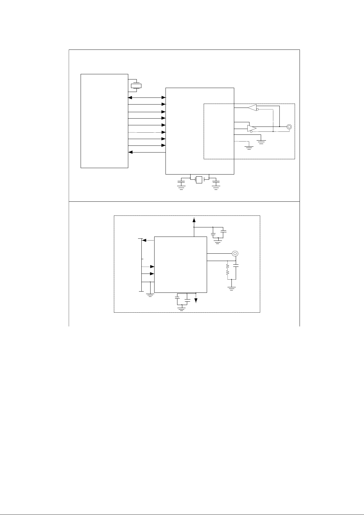
FIGURE 3 - NON-MULTIPLEXED, 6801-LIKE BUS INTERFACE WITH RS-485 INTERFACE
D0-D7
nIRQ1
nRES
nIOS
R/nW
A7
D0-D7
A0/nMUX
A0
XTAL1
XTAL2
A1
A1
nCS
nRESET
nRD/nDS
nWR/nDIR
nINTR
A2/BALE
A2
RXIN
nPULSE1
nPULSE2
TXEN
GND
Differential Driver
Configuration
6801
COM20020
Media Interface
may be replaced
with Figure A, B or C.
*
75176B or
Equiv.
XTA
L
1XTAL
2
27 pF 27 pF
20M
H
z
XTAL
RXIN
nPULSE1
nPULSE2
nTXEN
GND
Traditional Hybrid
Configuration
RXIN
nPULSE1
nPULSE2
17, 19,
4, 13, 14
5.6K
1/2W
5.6K
1/2W
0.01 uF
1KV
12
11
-5V
0.47
uF
10
uF
+
3
0.47
uF
+
+5V
uF
10
6
FIGURE C
HYC9088
HYC9068 or
N/C
*Valid for 2.5 Mbps only.

16
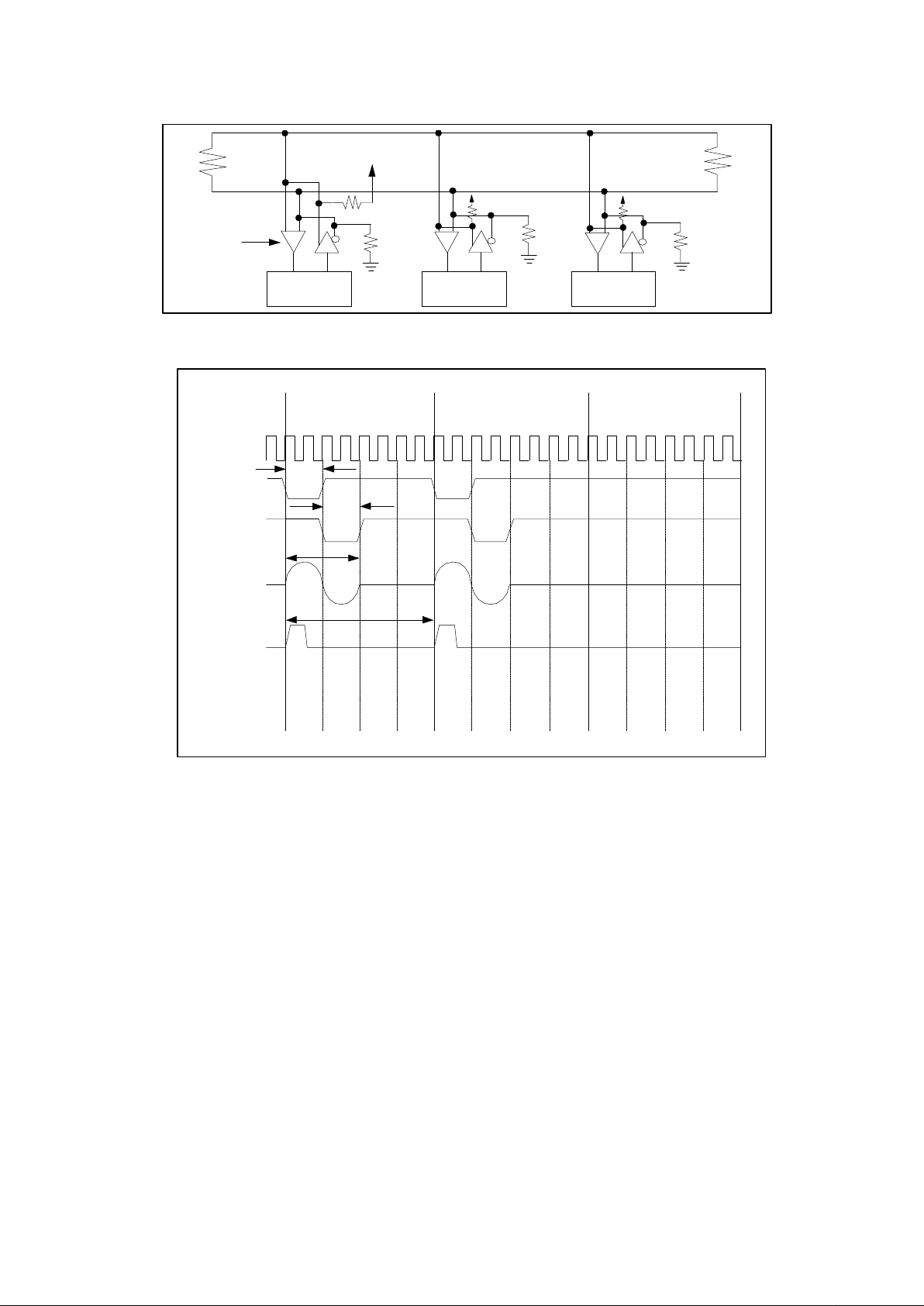
High Speed CPU Bus Timing Support
High speed CPU bus support was added to the
COM20020D. The reasoning behind this is as
follows: With the Host interface in Nonmultiplexed Bus mode, I/O address and Chip
Select signals must be stable before the read
signal is active and remain after the read signal
is inactive. But the High Speed CPU bus timing
doesn't adhere to these timings. For example, a
RISC type single chip microcontroller (like the
HITACHI SH-1 series) changes I/O address at
the same time as the read signal. Therefore,
several external logic ICs would be required to
connect to this microcontroller.
In addition, the Diagnostic Status (DIAG) register
is cleared automatically by reading itself. The
internal DIAG register read signal is generated
by decoding the Address (A2-A0), Chip Select
(nCS) and Read (nRD) signals. The decoder will
generate a noise spike at the above tight timing.
The DIAG register is cleared by the spike signal
without reading itself. This is unexpected
operation. Reading the internal RAM and Next
Id Register have the same mechanism as
reading the DIAG register.
Therefore, the address decode and host
interface mode blocks were modified to fit the
above CPU interface to support high speed CPU
bus timing. In Intel CPU mode (nRD, nWR
mode), 3 bit I/O address (A2-A0) and Chip Select
(nCS) are sampled internally by Flip-Flops on the
falling edge of the internal delayed nRD signal.
The internal real read signal is the more delayed
nRD signal. But the rising edge of nRD doesn't
delay. By this modification, the internal real
address and Chip Select are stable while the
internal real read signal is active. Refer to figure
4 below.
FIGURE 4 - HIGH SPEED CPU BUS TIMING - INTEL CPU MODE
The I/O address and Chip Select signals, which
are supplied to the data output logic, are not
sampled. Also, the nRD signal is not delayed,
because the above sampling and delaying paths
decrease the data access time of the read cycle.
The above sampling and delaying signals are
supplied to the Read Pulse Generation logic
which generates the clearing pulse for the
Diagnostic register and generates the starting
pulse of the RAM Arbitration. Typical delay time
between nRD and nRD1 is around 15nS and
between nRD1 and nRD2 is around 10nS.
Longer pulse widths are needed due to these
delays on nRD signal. However, the CPU can
insert some wait cycles to extend the width
without any impact on performance.
A2-A0, nCS
nRD
Delayed nRD
(nRD1)
Sampled A2-A0, nCS
More delayed nRD
(nRD2)
VALID
VALID

17
The RBUSTMG bit was added to Disable/Enable
the High Speed CPU Read function. It is defined
as: RBUSTMG=0, Disabled (Default);
RBUSTMG=1, Enabled.
In the MOTOROLA CPU mode (DIR, nDS
mode), the same modifications apply.
RBUSTMG BIT BUS TIMING MODE
0 Normal Speed CPU Read and Write
1 High Speed CPU Read and Normal Speed CPU Write
TRANSMISSION MEDIA INTERFACE
The bottom halves of Figures 2 and 3 illustrate the
COM20020D interface to the transmission media
used to connect the node to the network. Table 1
lists different types of cable which are suitable for
ARCNET applications.1 The user may interface to
the cable of choice in one of three ways:
Traditional Hybrid Interface
The Traditional Hybrid Interface is that which is
used with previous ARCNET devices. The Hybrid
Interface is recommended if the node is to be
placed in a network with other Hybrid-Interfaced
nodes. The Traditional Hybrid Interface is for use
with nodes operating at 2.5 Mbps only. The
transformer coupling of the Hybrid offers isolation
for the safety of the system and offers high
Common Mode Rejection. The Traditional Hybrid
Interface uses circuits like SMSC's HYC9068 or
HYC9088 to transfer the pulse-encoded data
between the cable and the COM20020D. The
COM20020D transmits a logic "1" by generating
two 100nS non-overlapping negative pulses,
nPULSE1 and nPULSE2. Lack of pulses
indicates a logic "0". The nPULSE1 and nPULSE2
signals are sent to the Hybrid, which creates a
200nS dipulse signal on the media. A logic "0" is
transmitted by the absence of the dipulse. During
reception, the 200nS dipulse appearing on the
media is coupled through the RF transformer of
the LAN Driver, which produces a positive pulse at
the RXIN pin of the COM20020D. The pulse on
the RXIN pin represents a logic "1". Lack of pulse
represents a logic "0". Typically, RXIN pulses
occur at multiples of 400nS. The COM20020D
can tolerate distortion of plus or minus 100nS and
still correctly capture and convert the RXIN pulses
to NRZ format. Figure 5 illustrates the events
which occur in transmission or reception of data
consisting of 1, 1, 0.
1
Please refer to TN7-5 – Cabling Guidelines for
the COM20020 ULANC, available from SMSC, for
recommended cabling distance, termination, and
node count for ARCNET nodes.

18
Backplane Configuration
The Backplane Open Drain Configuration is
recommended for cost-sensitive, short-distance
applications like backplanes and instrumentation.
This mode is advantageous because it saves
components, cost, and power.
Since the Backplane Configuration encodes data
differently than the traditional Hybrid
Configuration, nodes utilizing the Backplane
Configuration cannot communicate directly with
nodes utilizing the Traditional Hybrid
Configuration. The Backplane Configuration does
not isolate the node from the media nor protects it
from Common Mode noise, but Common Mode
Noise is less of a problem in short distances.
The COM20020D supplies a programmable
output driver for Backplane Mode operation. A
push/pull or open drain driver can be selected by
programming the P1MODE bit of the Setup 1
Register (see register descriptions for details).
The COM20020D defaults to an open drain
output.
The Backplane Configuration provides for direct
connection between the COM20020D and the
media. Only one pull-up resistor (in open drain
configuration of the output driver) is required
somewhere on the media (not on each individual
node). The nPULSE1 signal, in this mode, is an
open drain or push/pull driver and is used to
directly drive the media. It issues a 200nS
negative pulse to transmit a logic "1". Note that
when used in the open-drain mode, the
COM20020D does not have a fail/safe input on
the RXIN pin. The nPULSE1 signal actually
contains a weak pull-up resistor. This pull-up
should not take the place of the resistor required
on the media for open drain mode.
19
FIGURE 5 - COM20020 NETWORK USING RS-485 DIFFERENTIAL TRANSCEIVERS
FIGURE 6 - DIPULSE WAVEFORM FOR DATA OF 1-1-0
COM20020
+VCC
RBIAS
+VCC +VCC
RBIAS
RBIAS
RT RT
75176B or
Equiv.
COM20020 COM20020
20MHZ
CLOCK
(FOR REF.
ONLY)
nPULSE1
nPULSE2
DIPULSE
RXIN
1 0
100ns
100ns
200ns
400ns
1

20
In typical applications, the serial backplane is
terminated at both ends and a bias is provided by
the external pull-up resistor.
The RXIN signal is directly connected to the cable
via an internal Schmitt trigger. A negative pulse
on this input indicates a logic "1". Lack of pulse
indicates a logic "0". For typical single-ended
backplane applications, RXIN is connected to
nPULSE1 to make the serial backplane data line.
A ground line (from the coax or twisted pair)
should run in parallel with the signal. For
applications requiring different treatment of the
receive signal (like filtering or squelching),
nPULSE1 and RXIN remain as independent pins.
External differential drivers/receivers for increased
range and common mode noise rejection, for
example, would require the signals to be
independent of one another. When the device is
in Backplane Mode, the clock provided by the
nPULSE2 signal may be used for encoding the
data into a different encoding scheme or other
synchronous operations needed on the serial data
stream.
Differential Driver Configuration
The Differential Driver Configuration is a special
case of the Backplane Mode. It is a dc coupled
configuration recommended for applications like
car-area networks or other cost-sensitive
applications which do not require direct
compatibility with existing ARCNET nodes and do
not require isolation.
The Differential Driver Configuration cannot
communicate directly with nodes utilizing the
Traditional Hybrid Configuration. Like the
Backplane Configuration, the Differential Driver
Configuration does not isolate the node from the
media.
The Differential Driver interface includes a RS485
Driver/Receiver to transfer the data between the
cable and the COM20020D. The nPULSE1 signal
transmits the data, provided the Transmit Enable
signal is active. The nPULSE1 signal issues a
200nS (at 2.5Mbps) negative pulse to transmit a
logic "1". Lack of pulse indicates a logic "0". The
RXIN signal receives the data, the transmitter
portion of the COM20020D is disabled during
reset and the nPULSE1, nPULSE2 and nTXEN
pins are inactive.
Programmable TXEN Polarity
To accommodate transceivers with active high
ENABLE pins, the COM20020D contains a
programmable TXEN output. To program the
TXEN pin for an active high pulse, the nPULSE2
pin should be connected to ground. To retain the
normal active low polarity, nPULSE2 should be
left open. The polarity determination is made at
power on reset and is valid only for Backplane
Mode operation. The nPULSE2 pin should
remain grounded at all times if an active high
polarity is desired.
21
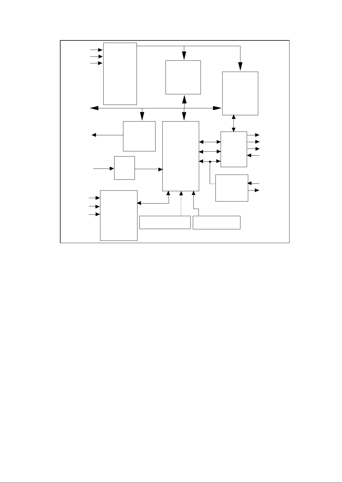
FIGURE 7 - INTERNAL BLOCK DIAGRAM
MICRO-
SEQUENCER
AND
WORKING
REGISTERS
STATUS/
COMMAND
REGISTER
RESET
LOGIC
RECONFIGURATION
TIMER
NODE ID
LOGIC
OSCILLATOR
TX/RX
LOGIC
ADDITIONAL
REGISTERS
ADDRESS
DECODING
CIRCUITRY
2K x 8
AD0-AD2,
BUS
ARBITRATION
CIRCUITRY
nPULSE1
nPULSE2
nTXEN
nINTR
nRESET
RAM
A0/
n
M
U
X
A
1
A2/
B
A
L
E
nRD/nDS
nWR/DIR
nCS
D3-D7
RXIN
XTAL1
XTAL2

22
Table 1 - Typical Media
CABLE TYPE
NOMINAL
IMPEDANCE
ATTENUATION PER 1000 FT.
AT 5 MHz
RG-62 Belden #86262
93Ω
5.5dB
RG-59/U Belden #89108
75Ω
7.0dB
RG-11/U Belden #89108
75Ω
5.5dB
IBM Type 1* Belden #89688
150Ω
7.0dB
IBM Type 3* Telephone Twisted
Pair Belden #1155A
100Ω
17.9dB
COMCODE 26 AWG Twisted
Pair Part #105-064-703
105Ω
16.0dB
*Non-plenum-rated cables of this type are also available.
Note: For more detailed information on Cabling options including RS-485, transformer-coupled RS-485
and Fiber Optic interfaces, please refer to TN7-5 – Cabling Guidelines for the COM20020 ULANC,
available from Standard Microsystems Corporation.
FUNCTIONAL DESCRIPTION
MICROSEQUENCER
The COM20020D contains an internal
microsequencer which performs all of the control
operations necessary to carry out the ARCNET
protocol. It consists of a clock generator, a 544 x
8 ROM, a program counter, two instruction
registers, an instruction decoder, a no-op
generator, jump logic, and reconfiguration logic.
The COM20020D derives a 10 MHz and a 5 MHz
clock from the output clock of the Clock Multiplier.
These clocks provide the rate at which the
instructions are executed within the COM20020D.
The 10 MHz clock is the rate at which the program
counter operates, while the 5 MHz clock is the rate
at which the instructions are executed. The
microprogram is stored in the ROM and the
instructions are fetched and then placed into the
instruction registers. One register holds the
opcode, while the other holds the immediate data.
Once the instruction is fetched, it is decoded by
the internal instruction decoder, at which point the
COM20020D proceeds to execute the instruction.
When a no-op instruction is encountered, the
microsequencer enters a timed loop and the
program counter is temporarily stopped until the
loop is complete. When a jump instruction is
encountered, the program counter is loaded with
the jump address from the ROM. The
COM20020D contains an internal reconfiguration
timer which interrupts the microsequencer if it has
timed out. At this point the program counter is
cleared and the MYRECON bit of the Diagnostic
Status Register is set.
 Loading...