

Standard Microsystems Corporation CAM35C44 Datasheet

CAM35C44
ADVANCE INFORMATION
Infrared Communications Controller Chip
CameraFR
FEATURES
!"
Mixed Voltage Support
- Supports 3.3V Operation
- Supports Mixed Internal 3.3V
Operation with 3.3V/5V External
Configuration
!"
Intelligent Auto Power Management
- Supports Multiple Power Down
Modes
!"
Serial Port
- High Speed NS16C550A Compatible
UART with 16-Byte Send/Receive
FIFOs
- Programmable Baud Rate Generator
!"
Infrared Port
- Multi-Protocol Infrared Interface
- 128-Byte Data FIFO
- IrDA 1.1 Compliant (up to 4Mbps)
- Consumer IR
- SHARP ASK IR
- Programmed I/O and DMA Options
GENERAL DESCRIPTION
The CAM35C44 with IrDA v1.1 (4Mbps) and
Consumer IR support incorporates SMSC’s
advanced Infrared Communications Controller
(IrCC 2.0), a 16C550A-compatible UART,
Multiple Host Interface options, flexible Address
Decoding and up to five General Purpose I/Os.
!"
!"
- ISA-Style 5 Bit Address and 8 Bit
Data Bus
- IOCHRDY and No Wait State Support
for Fast IR
- Non-ISA 8 Bit Multiplexed
Address/Data Bus
- Programmable Read/Write Interface
- One 8 Bit DMA Channel
- One Programmable IRQ
- Chip Select
- Multihost Interface Support Includes
Hitachi and Mitsubishi
Microcontrollers
!"
- Supports Internal or External Clock
Source
!"
The CAM35C44 also features sophisticated
power control circuitry to support multiple power
down modes, an on-chip 24MHz crystal
oscillator, and
The CAM35C44 is particularly suited for 3.3v
battery-powered systems.
Up to 5 General Purpose I/O Pins
Programmable Multi-Protocol Host Interface
24MHz Crystal Oscillator
48 Pin TQFP Package
12mA
host bus drivers.

TABLE OF CONTENTS
FEATURES.............................................................................................................................................. 1
GENERAL DESCRIPTION......................................................................................................................1
ARCHITECTURE.....................................................................................................................................4
PIN CONFIGURATION............................................................................................................................5
DESCRIPTION OF PIN FUNCTIONS......................................................................................................6
UFFER-TYPE SUMMARY
B
........................................................................................................................... 11
CLOCK GENERATOR........................................................................................................................... 12
MULTIHOST CPU INTERFACE............................................................................................................ 13
OST INTERFACE SELECT
H
OST INTERFACE PIN MULTIPLEXING
H
.......................................................................................................................... 14
........................................................................................................... 14
System Data Bus ................................................................................................................................... 14
ISA Address Bus SA0 - SA1..................................................................................................................15
ISA Address Bus SA2 - SA4..................................................................................................................15
ISA nIOR................................................................................................................................................15
ISA nIOW...............................................................................................................................................15
REGISTER ADDRESS MAP..................................................................................................................16
ULTIPLEXED
NON-M
ULTIPLEXED ADDRESSING
M
DDRESSING
(ISA) A
....................................................................................................... 16
........................................................................................................................ 17
CONFIGURATION.................................................................................................................................18
ONFIGURATION ACCESS PORTS
C
ONFIGURATION STATE
C
ONFIGURATION REGISTERS
C
............................................................................................................................. 19
................................................................................................................ 18
...................................................................................................................... 21
INFRARED INTERFACE.......................................................................................................................30
IRDA SIR/FIR ......................................................................................................................................... 30
ASKIR .................................................................................................................................................... 30
ONSUMER
C
ARDWARE INTERFACE
H
IR.......................................................................................................................................... 30
............................................................................................................................. 30
GENERAL PURPOSE I/O ..................................................................................................................... 32
NTRODUCTION
I
ESCRIPTION
D
EGISTERS
R
..........................................................................................................................................32
............................................................................................................................................32
..............................................................................................................................................34
DC ELECTRICAL CHARACTERISTICS............................................................................................... 36
A.C. TIMING .......................................................................................................................................... 38
LOCK AND RESET TIMING
C
EAD CYCLE TIMING (NON-MULTIPLEXED
R
EAD CYCLE TIMING (MULTIPLEXED
R
RITE CYCLE TIMING (NON-MULTIPLEXED
W
RITE CYCLE TIMING (MULTIPLEXED
W
......................................................................................................................... 38
)................................................................................................... 39
)........................................................................................................... 40
)................................................................................................. 41
)......................................................................................................... 42
2

EAD/WRITE CYCLE TIMING (MULTIPLEXED
R
INGLE TRANSFER MODE
S
URST TRANSFER MODE
B
DMA T
DMA T
IMING
IMING
)................................................................................................43
....................................................................................................... 44
........................................................................................................ 46
3
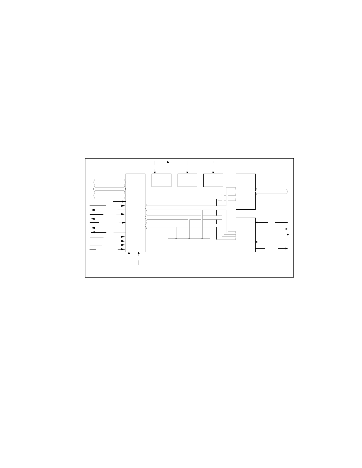
ARCHITECTURE
There are six basic architectural components in
the CAM35C44: the multihost CPU interface, the
IrCC 2.0, a clock generator, configuration
registers, power management, and general
purpose I/O (
FIGURE
The multihost CPU interface is capable of
supporting several bus configurations; including,
a non-multiplexed ISA-style address and data
bus, and a multiplexed address/data bus with
selectable read/write command options. The
multihost CPU interface includes support for
Hitachi and Mitsubishi microcontrollers.
1
).
nIOW/DSTRB
SD[7:0]/AD[7:0]
SA[1:0]/GPIO[4:3]
SA[4:2]/BS[2:0]
nCS
AEN
IOCHRDY
ASTRB
nNOWS
RESET_DRV
IRQ
DRQ
nDACK
TC
nIOR/RW
X1/CLK1 x2 PWRGD
CLOCK
GEN
MULTIHOST
CPU
INTERFACE
HS1 HS0
CONTROL
ADDRESS
CONFIGURATION
FIGURE 1 - CAM35C44 BLOCK DIAGRAM
The IrCC 2.0 is a multi-protocol serial
communications controller that incorporates an
ACE 16C550A UART and a Synchronous
Communications Engine (SCE). Refer to the
SMSC Infrared Communications Controller 2.0
specification for more information.
The clock generator provides connections for a
24MHz crystal or an external clock source. The
24MHz clock directly drives the ACE block. An
internal PLL is used for data rates above
115.2Kbps.
Power management in the CAM35C44 includes
various power down modes and an infrared
wake-up option. The general purpose I/O
interface provides generic I/O programming
capabilities.
VCC[2:1],VSS[3:1],
POWER
MGMT
VIO
POWER
GENERAL
PURPOSE
I/O
GPIO[2:0]
DATA
REGISTERS
IRCC 2.0
IRRX
IRTX
IRMODE/IRRX3
RXD/IRRX
TXD/IRTX
4
PIN CONFIGURATION
The CAM35C44 pin numbers are shown in
FIGURE 2. Functional descriptions per pin-
N/C
SA2/BS2
SA1/GP IO4
SA0/GP IO3
PWRG D
48
47
46
45
SA3/BS1
SA4/BS0
TXD/IRTX
IRTX
IRMODE/IRRX3
VIO
nIOR/RnW
nIOW/DSTRB
nNOWS
AEN
nCS
N/C
1
2
3
4
5
6
7
8
9
10
11
12
13
N/C
48 PI N T QFP
14
15
SD0/AD0
SD1/AD1
FIGURE 2 - CAM35C44 PIN CONFIGURATION
44
CAM35C44
16
17
SD2/AD2
SD3/AD3
group are shown in TABLE 1.
Note: The pin numbers in FIGURE 2 are subject
to change.
VSS
ASTRB
VDD
GPIO2
GPIO1
GPIO0
VSS
43
42
41
40
39
38
37
HS1
36
HS0
35
X2
34
X1/CLK1
33
IRRX
18
19
20
21
22
32
RXD/IRRX
31
TC
30
IOCHRDY
29
RESET_DRV
28
VDD
27
nDAC K
26
N/C
25
23
24
SD4/AD4
SD5/AD5
SD6/AD6
SD7/AD7
IRQ
VSS
DRQ
5

DESCRIPTION OF PIN FUNCTIONS
TABLE 1 - CAM35C44 PIN FUNCTION DESCRIPTION
NAME
ISA System Data Bus/
Multiplexed
Address/Data Bus
(Non-ISA)
ISA System Address
Bus (SA0 - SA1)/
General Purpose I/O
(GPIO3 - GPIO4)
ISA System Address
Bus (SA2 - SA4)/
Memory Block Selects
(BS0 - BS2)
Chip Select 1 nCS I The active low chip select input is
4
TOTAL
PINS
PROCESSOR/HOST INTERFACE (25)
8 SD[7:0]/AD[7:0] IO12 T his 8 bit bus is used to exchange
2 SA[1:0]/GPIO[4:3] I/IO12 The ISA system address bus is
3 SA[4:2]/BS[2:0] I The ISA system address bus is
SYMBOL
BUFFER
TYPE
DESCRIPTION
data with the host. The bus is bidirectional and can be configured
as either an ISA system data bus
or as a multiplexed address/data
bus (TABLE 3). These pins are in
a high-impedance state when not
in the output mode.
used to determine the I/O address
during read and write cycles.
These two ISA system address
bus pins are general purpose I/O
pins (TABLE 30) when a
multiplexed address/data host
interface type is selected (TABLE
3).
used to determine the I/O address
during read and write cycles.
These three ISA system address
bus pins are memory block select
pins (TABLE 10) when a
multiplexed address/data host
interface type is selected (TABLE
3).
a 32-byte address block decoder
when the ISA host interface type
is selected and a 256-byte page
decoder when a multiplexed
address/data host interface type is
selected (TABLE 3).
6

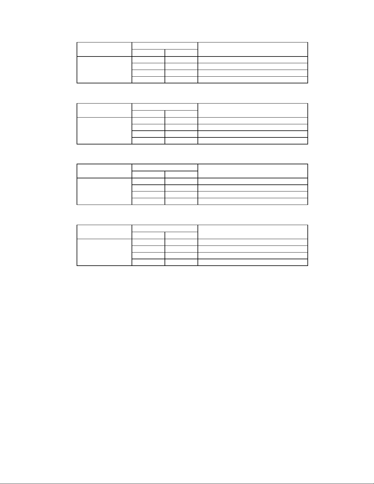
NAME
Address Enable 1 AEN I The active high Address Enable
ISA I/O Channel Ready 1 IOCHRDY OD12 IOCHRDY is pulled low to extend
Multiplex Mode
Address Strobe
No Wait State 1 nNOWS OD12 nNOWS can be enabled to be
ISA Reset Drive 1 RESET_DRV IS The RESET_DRV pin is active
IRQ
TOTAL
PINS
1 ASTRB I ASTRB is used to internally latch
1 IRQ
SYMBOL
BUFFER
TYPE
pin indicates DMA operations on
the host data bus. AEN must be
inactive to access the CAM35C44
registers and active during DMA
operations regardless of the
selected host interface type.
ISA I/O read/write commands.
Only SCE-driven functions in the
IrCC 2.0 can be enabled to use
IOCHRDY.
I/O addresses during read/write
cycles when a multiplexed
address/data host interface type is
selected (TABLE 3).
activated by IrCC 2.0 SCE-driven
functions to indicate that an
access cycle shorter than the
standard ISA I/O cycle can be
executed.
high and is used to reset the
CAM35C44 as described in the
appropriate sections in this
document. The configuration
registers are not affected by this
pin except where noted (TABLE
13). The RESET_DRV pin must
be valid for 500ns minimum.
OD12 The IRQ pin is forced active when
an interrupt is asserted. IRQ goes
inactive as soon as the source of
the interrupt has been cleared.
The active IRQ pin-state is
determined by the IRQ_LEV bit in
CR00 (see page 22).
DESCRIPTION
7

NAME
DMA Request 1 DRQ O12 The DRQ pin is forced active by
DMA Acknowledge 1 DACK I The DACK pin is forced active by
Terminal Count 1 TC I TC indicates that a DMA transfer
ISA I/O Read/
Non-ISA Read/Write
Control
ISA I/O Write/
Non-ISA R/W Data
Strobe
TOTAL
PINS
1 nIOR/RnW I The active low nIOR input is
1 nIOW/DSTRB I The active low nIOW input is
SYMBOL
BUFFER
TYPE
DESCRIPTION
the CAM35C44 when byte
transfers to the host using DMA
are required. DRQ goes inactive
when the transfer has been
completed. The active DRQ pinstate is determined by the
DRQ_LEV bit in CR01 (see page
22).
the host DMA controller to
acknowledge CAM35C44 transfer
requests. DACK goes inactive
following the transfer command.
The active DACK pin-state is
determined by the DAC_LEV bit in
CR01 (see page 23).
is complete. TC is only acknowledged when DACK is active.
issued by the host to execute I/O
read commands when an ISA
read/write-styled host interface
type is selected (TABLE 3). The
RnW input is used to determine
the I/O command type when a
non-ISA read/write-styled host
interface type is selected.
issued by the host to execute I/O
write commands when an ISA
read/write-styled host interface
type is selected (TABLE 3). The
DSTRB input is used to execute
the I/O command when a non-ISA
read/write-styled host interface
type is selected (FIGURE 5).
MISCELLANEOUS (12)
8

NAME
Clock Input (24MHz
CMOS Clock/Crystal)
Crystal Driver 1 X2 OCLK X2 is the 24M H z cry stal driver and
Host Interface Select 2 HS[1:0] IP The Host Interface Select bits
General Purpose I/O
(GPIO0 - GPIO2)
4
TOTAL
PINS
SYMBOL
BUFFER
TYPE
DESCRIPTION
1 X1/CLK1 ICLK X1/CLK is the input for either a
24MHz clock crystal or 24MH z
crystal oscillator source (see
section CLOCK GENERATOR on
page 12)
should be left unconnected if an
external clock source is used.
determine the host interface type.
These bits are static controls and
must remain stable during device
operation (see section
MULTIHOST CPU INTERFACE
on page 13).
3 GPIO[2:0] IO12 The general purpose I/O pins
provide a simple programmable
I/O interface. The state of a GPIO
pin can be forced to the value
contained in the GPIO data
register or this register can reflect
the logical state of the GPIO pin
depending on values programmed
in GPIO direction and enable
registers (see section GENERAL
PURPOSE I/O on page 32).
9
NAME
Power Good 1 PWRGD IP This active high input indicates
No Connect 4 N/C - No internal connections are made
Infrared Rx3 1 IRRX I This is the infrared port receiver
Infrared Tx
1,2
1 IRTX O12PD This is the infrared port transmitter
Infrared Mode/IRRX31 1 IRMODE/IRRX3 O12/I This is the infrared port secondary
+3.3V Digital Supply
Voltage
I/O Interface Supply
Voltage
1
Ground 3 VSS Ground Supply
TOTAL
PINS
SYMBOL
BUFFER
TYPE
DESCRIPTION
that the positive supply voltage
VCC is valid. For normal device
operation, PWRGD must be
active. When PWRGD is inactive,
all device inputs are disconnected
and placed into a low power state;
all outputs are put into a highimpedance state.
Note: The
crystal oscillator pins are
unaffected by PWRGD
contents of all registers are
preserved as long as VCC has a
valid value. Output driver current
drain when PWRGD is inactive
drops to I
- standby current.
STDBY
The PWRGD input has an internal
30#A pull-up.
to these pins.
INFRARED INTERFACE (3)
input pin.
output pin.
receiver input channel or a
transceiver mode control pin,
depending on the state of the
transceiver module interface type
select ( T ABLE 27).
POWER PINS (6)
2 VCC Positive Supply Voltage
1 VIO Positive I/O Interface Supply
Voltage
. The
10
NAME
Receive Serial Data 2/
3
Infrared Rx
Transmit Serial Data
2/Infrared Tx
Note
Note
Note
Note
1,2
1
TX and MODE pins drive to VIO level.
2
TX defaults to zero even during POR.
3
RX pins are voltage tolerant to VIO level.
4
All GPIOs are VIO tolerant and back drive protected.
Buffer-Type Summary
The characteristics of the buffer types shown in TABLE 1 are summarized in TABLE 2.
BUFFER TYPE DESCRIPTION
IO12 Input/Output. 12mA sink; 6mA source
O12 Output. 12mA sink; 6mA source
OD12 Open Drain. 12mA sink
O12PD
ICLK Input to Crystal Oscillator Circuit (TTL levels)
OCLK Output to External Crystal
I Input TTL Compatible.
IP
IS Input with Schmitt Trigger.
TOTAL
PINS
SERIAL PORT INTERFACE (2)
1 RXD/IRRX I This is the receiver input pin for
1 TXD/IRTX O12PD This is the transmitter output pin
TABLE 2 - CAM35C44 BUFFER-TYPE SUMMARY
Output. 12mA sink; 6mA source; 30#A Pulldown @ Tristate
Input TTL Compatible with 30#A Pullup
SYMBOL
BUFFER
TYPE
DESCRIPTION
the UART COM port or an
alternate infrared port receiver
input.
for the UART COM port or an
alternate infrared port transmitter
output.
11
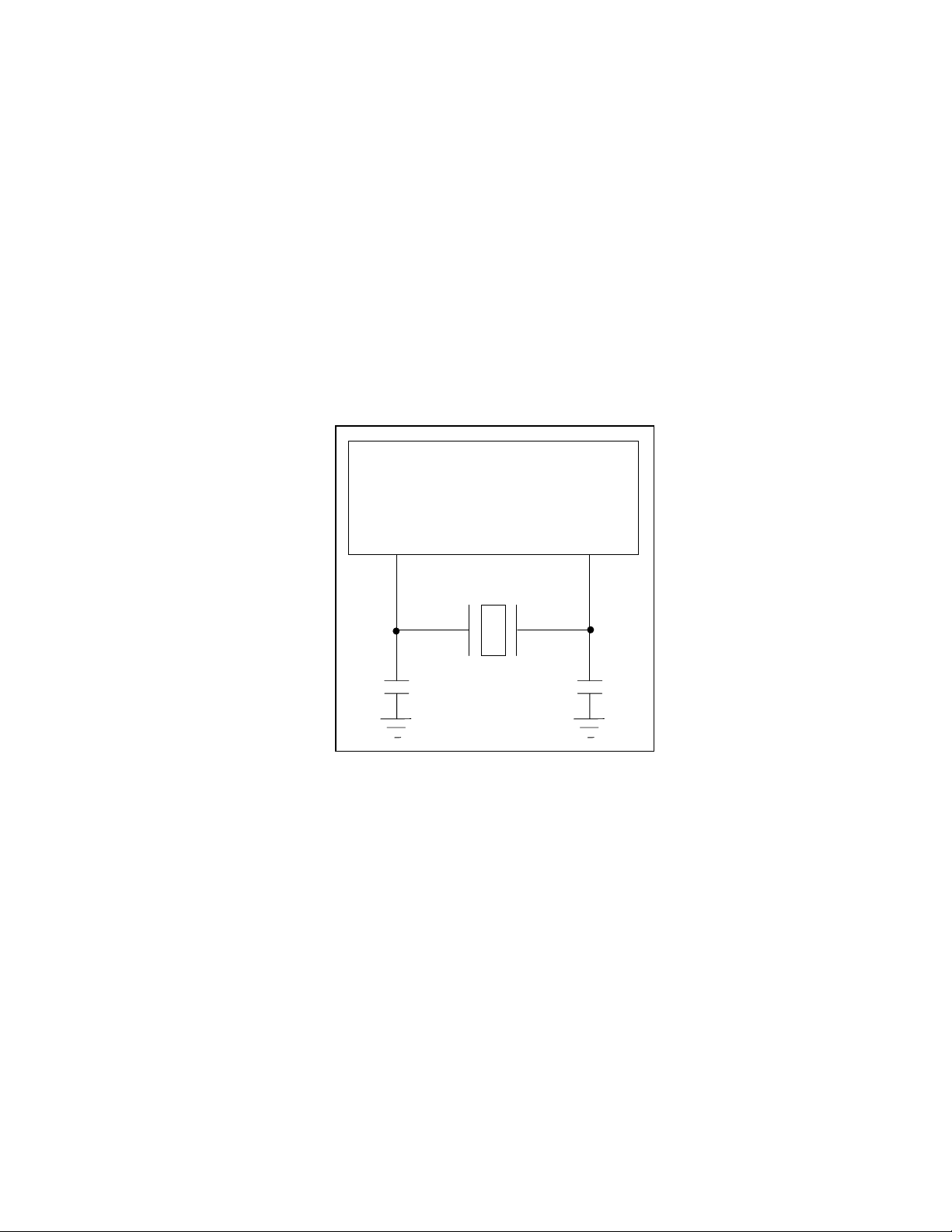
CLOCK GENERATOR
An internal 3.3v crystal oscillator or an external
oscillator source is required for the CAM35C44
(FIGURE 3). The crystal/clock pins and buffer
types are shown in TABLE 1.
The X1/CLK1 and X2 pins provide an external
connection for a parallel resonant 24MHz crystal.
Configuration register CR08 bit 5, INT_OSC,
must be set to “1” to configure the internal
oscillator for this arrangement (see the section
CRO8 - Power Control on page 27).
An external CMOS compatible oscillator is
required if a 24MHz crystal is not used. In this
case INT_OSC must be set to “0”.
FIGURE 3 - EXAMPLE 24MHz OSCILLATOR CIRCUIT
CAM35C44
The X2 pin is the 24MHz crystal driver and
should not be used to drive any other device.
This pin should be left unconnected if an
external clock is used and INT_OSC is “0”.
The 24MHz crystal can be used to directly drive
the ACE block. This saves power when
115.2Kbps or slower data transfers are required
because the PLL and SCE block do not need to
be powered. See TABLE 25 and the section
CRO8 - Power Control on page 27.
X1/CLK1 X2
24MHz CRYSTAL
12
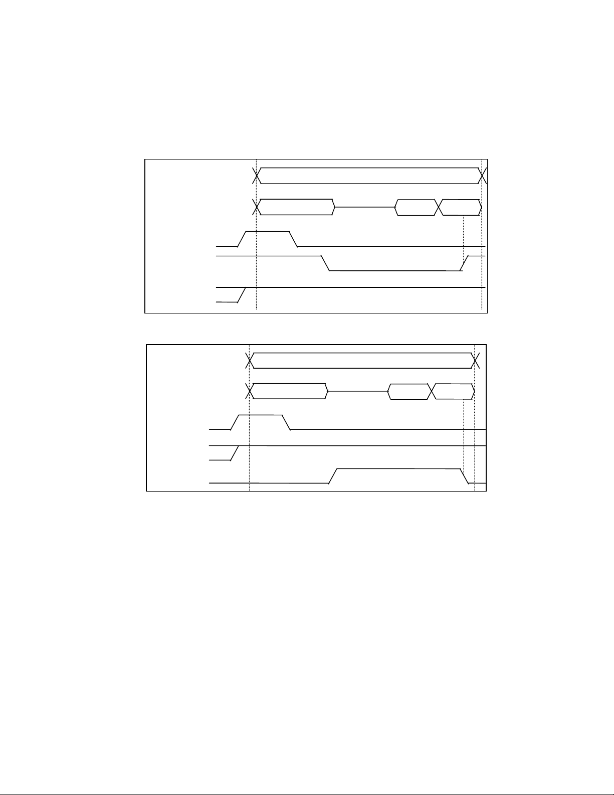
MULTIHOST CPU INTERFACE
The CAM35C44 multihost CPU interface is
capable of supporting three bus configurations;
including, 1) an ISA-style address and data bus,
2) a multiplexed address/data bus with ISA-style
read/write commands like the example shown in
(FIGURE 4, and 3) a multiplexed address/data
FIGURE 4 - NEC UPD781C1X READ CYCLE
bus with a read/write select and data strobe like
the example shown in FIGURE 5.
The CPU interface type as well as the typespecific multiplexing of the processor/host
interface pins (TABLE 1) is controlled by the
Host Interface Select pins.
AB[15:8]
AB[7:0]
ADDR7-ADDR
ADDR15-ADDR
0
8
Data In
ADDR STB
nRD
nWR
AB[15:8]
AB[7:0]
ADDR7-ADD R
ADDR15-ADD R
0
8
Data In
ADDR STB
R/nW
DATA STB
FIGURE 5 - HITACHI HD63P01M1 READ CYCLE
13
Host Interface Select
The Host Interface Select pins HS[1:0] (TABLE
1) determine the host interface type.
TABLE 3 - HOST INTERFACE ENCODING
HOST INTERFACE
SELECT
HS1
0 0 Reserved
0 1 ISA
1 0 MULTIPLEXED ADDRESS/DATA, Non-ISA
1 1 MULTIPLEXED ADDRESS/DATA,
Host Interface Pin Multiplexing
Pin multiplexing for the processor/host interface
(TABLE 1) is controlled by the Host Interface
Select pins HS[1:0].
System Data Bus
PIN NAME
SD[7:0] 0 0 NOT DEFINED
0 1 SD[7:0]
1 0 AD[7:0]
1 1 AD[7:0]
HS0
TABLE 4 - SD[7:0] PIN MULTIPLEXING
MUX CONTROLS
HS1
Read/Write (FIGURE 5)
ISA Read/Write (FIGURE 4)
HS0
The encoding for these bits is shown in TABLE
3. The Host Interface Select pins are static
controls and must remain stable during device
operation.
HOST INTERFACE TYPE
ISA signals that are not multiplexed, like
IOCHRDY and nNOWS, remain operative
regardless of the state of the Host Interface
Select bits.
The following tables describe processor/host
interface multiplexing per pin or per pin group.
SELECTED FUNCTION
14
ISA Address Bus SA0 - SA1
TABLE 5 - SA[1:0] PIN MULTIPLEXING
PIN NAME
SA[1:0] 0 0 NOT DEFINED
0 1 SA[1:0]
1 0 GPIO[4:3]
1 1 GPIO[4:3]
ISA Address Bus SA2 - SA4
PIN NAME
SA[4:2] 0 0 NOT DEFINED
0 1 SA[4:2]
1 0 BS[2:0]
1 1 BS[2:0]
ISA nIOR
PIN NAME
nIOR 0 0 NOT DEFINED
0 1 nIOR
1 0 R/nW
1 1 nIOR
ISA nIOW
PIN NAME
nIOW 0 0 NOT DEFINED
0 1 nIOW
1 0 DSTRB
1 1 nIOW
MUX CONTROLS
HS1
TABLE 6 - SA[4:2] PIN MULTIPLEXING
MUX CONTROLS
HS1
TABLE 7 - nIOR PIN MULTIPLEXING
MUX CONTROLS
HS1
TABLE 8 - nIOW PIN MULTIPLEXING
MUX CONTROLS
HS1
HS0
HS0
HS0
HS0
SELECTED FUNCTION
SELECTED FUNCTION
SELECTED FUNCTION
SELECTED FUNCTION
15
 Loading...