

Standard Microsystems Corporation 82443BX Datasheet

Intel® 440BX AGPset:
82443BX Host Bridge/Controller
Datasheet
April 1998
Order Number: 290633-001

Information in this document is provided in connection with Intel products. No license, express or implied, by estoppel or otherwise, to any intellectual
property rights is granted by this document. Except as provided in Intel's Terms and Conditions of Sale for such products, Intel assumes no liability
whatsoever, and Intel disclaims any express or implied warranty, relating to sale and/or use of Intel products including liability or warranties relating to
fitness for a particular purpose, merchantability, or infringement of any patent, cop yright or other intellectual property right. Intel products are not
intended for use in medical, life saving, or life sustaining applications.
Intel may make changes to specifications and product descriptions at any time, without notice.
Contact your local Intel sales office or your distributor to obtain the latest specifications and before placing your product order.
The 82443BX chipset may contain design defects or errors known as errata which may cause the product to deviate from published specifications.
Current characterized errata are available upon request.
2
I
C is a two-wire communications bus/protocol developed by Philips. SMBus is a subset of the I2C bus/protocol and was developed by Intel.
Implementations of the I
North American Philips Corporation.
Copies of documents which have an ordering number and are referenced in this document, or other Intel literature may be obtained by:
calling 1-800-548-4725 or
by visiting Intel's website at http://www.intel.com.
Copyright © Intel Corporation, 1997-1998
*Third-party brands and names are the property of their respective owners.
2
C bus/protocol or the SMBus bus/protocol may require licenses from various entities, including Philips Electronics N.V. and
82443BX Host Bridge
Datasheet

Intel 82443BX Features
Processor/host bus support
•
— Optimized for Pentium
processor at 100 MHz system bus
frequency; Support for 66 MHz
— Supports full symmetric
Multiprocessor (SMP) Protocol for
up to two processors; I/O APIC
related buffer management support
(WSC# signal)
— In-order transaction and dynamic
deferred transaction support
— Desktop optimized GTL+ bus driv er
technology (gated GTL+ receivers
for reduced power)
Integrated DRAM controller
•
— 8 to 512 Mbytes or 1G B (with
registered DIMMs)
— Supports up to 4 double-sided
DIMMs (8 rows memory)
— 64-bit data interface with ECC
support (SDRAM only)
— Unbuffered and Registered
SDRAM (Synchronous) DRAM
Support (x-1-1-1 access @ 66 MHz,
x-1-1-1 access @ 100 MHz)
— Enhanced SDRAM Open Page
Architecture Support for 16- and
64-Mbit DRAM devi ces with 2k, 4k
and 8k page sizes
PCI bus interface
•
— PCI Rev. 2.1, 3.3V and 5V, 33MHz
interface compliant
— PCI Parity Generation Support
— Data streaming support from PCI to
DRAM
— Delayed Transaction support for
PCI-DRAM Reads
— Supports concurrent CPU, AGP and
PCI transactions to main memory
®
II
AGP interface
•
— Supports single AGP compliant
device (AGP-66/133 3.3V device)
— AGP Specification Rev 1.0
compliant
— AGP-data/transaction flow
optimized arbitration mechanism
— AGP side-band interface for ef fi cient
request pipelining without
interfering with the data streams
— AGP-specific data buffering
— Supports concurrent CPU, AGP and
PCI transactions to main memory
— AGP high-priority transactions
(“expedite”) support
Power Management Functions
•
— Stop Clock Grant and Halt special
cycle translation (host to PCI Bus)
— Mobile and “Deep Green” Desktop
support for system suspend/resume
(i.e., DRAM and power-on suspend)
— Dynamic power do wn of idle DRAM
rows
— SDRAM self-refresh power down
support in suspend mode
— Independent, internal dynam ic cl ock
gating reduces average power
dissipation
— Static STOP CLOCK support
— Power-on Suspend mode
— Suspend to DRAM
— ACPI compliant power management
Packaging/Voltage
•
—492 Pin BGA
— 3.3V core and mixed 3. 3V and GTL
I/O
Supporting I/O Bridge
•
— System Management Bus (SMB)
with support for DIMM Serial
Presence Detect (SPD)
— PCI-ISA Bridge (PIIX4E)
— Power Management Support
— 3.3V core and mixed 5V, 3.3V I/O
and interface to the 2.5V CPU
signals via open-drain output buffers
82443BX Host Bridge
The Intel® 440BX AGPset is intended for the Pentium® II processor platform and emerging 3D
graphics/multimedia applications. The 82443BX Host Bridge provides a Host-to-PCI bridge,
optimized DRAM controller and data path, and an Accelerated Graphic Port (AGP) interface.
AGP is a high performance, component level interconnect targeted at 3D graphics applications
and is based on a set of performance enhancements to PCI.
The Intel 82443BX may contain design defects or errors known as errata which may cause the products to deviate from
published specifications. Current characterized errata are available on request.
Datasheet
iii
The I/O subsystem portion o f the Intel® 440BX AGPset platform is based on the 82371EB
(PIIX4E), a highly integrated version of the Intel’s PCI-ISA bridge family. The Intel
AGPset is ideal for the Mobile AGPset Pentium II processor platforms; providing full support
for all system suspend modes and segmented power planes.
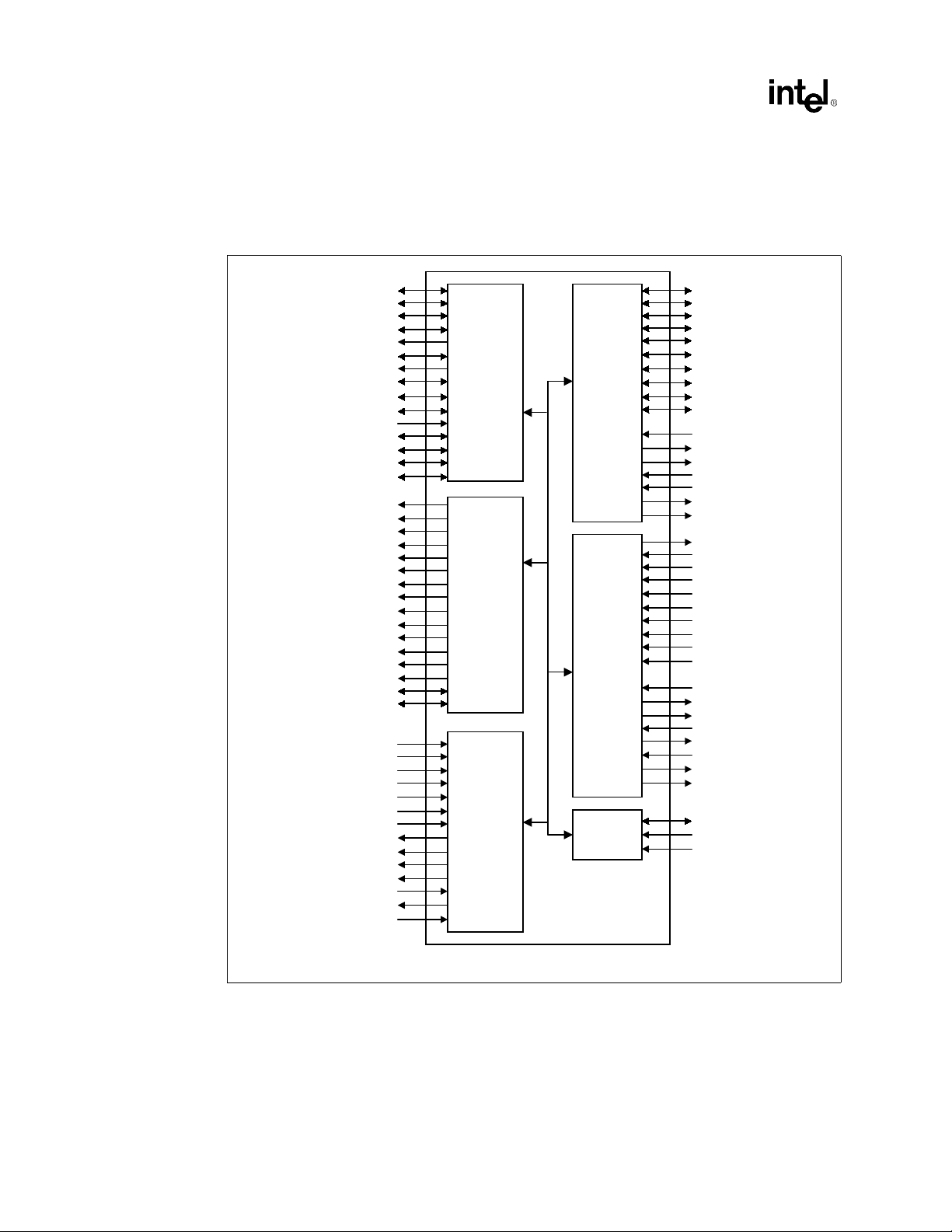
Intel 82443BX Simplified Block Diagram
®
440BX
A[31:3]#
ADS#
BPRI#
BNR#
CPURST#
DBSY#
DEFER#
HD[63:0]#
HIT#
HITM#
HLOCK#
HREQ[4:0]#
HTRDY#
DRDY#
RS[2:0]#
RASA[5:0]/CSA[5:0]#
RASB[5:0]/CSB[5:0]#
CKE[3:2]/CSA[7:6]#
CKE[5:4]/CSB[7:6]#
CASA[7:0]/DQMA[7:0]
CASB[5,1]/DQMB[5,1]
GCKE/CKE1
SRAS[B,A]#
CKE0/FENA
SCAS[B,A]#
MAA[13:0]
MAB[13,12#,11#,10,9#:0#]
WEA#
WEB#
MD[63:0]
MECC[7:0]
HCLKIN
PCLKIN
GTLREF[B:A]
AGPREF
VTT[B:A]
REF5V
PCIRST#
CRESET#
BREQ0#
TESTIN#
GCLKO
GCLKIN
DCLKO
DCLKWR
Host
Interface
DRAM
Interface
Clocks,
Reset,
Test,
and
Misc.
PCI Bus
Interface
(PCI #0)
AGP
Interface
Power
Mgnt
AD[31:0]
C/BE[3:0]#
FRAME#
TRDY#
IRDY#
DEVSEL#
PAR
SERR#
PLOCK#
STOP#
PHOLD#
PHLDA#
WSC#
PREQ0#
PREQ[4:1]#
PGNT0#
PGNT[4:1]#
GAD[31:0]
GC/BE[3:0]#
GFRAME#
GIRDY#
GTRDY#
GSTOP#
GDEVSEL#
GREQ#
GGNT#
GPAR
PIPE#
SBA[7:0]
RBF#
STOP#
ST[2:0]
ADSTB_A
ADSTB_B
SBSTB
CLKRUN#
SUSTAT#
BXPWROK
BX_BLK.VSD
iv
82443BX Host Bridge
Datasheet

Contents
1 Architectural Overview...............................................................................................1-1
2 Signal Description......................................................................................................2-1
2.1 Host Interface Signals...................................................................................2-1
2.2 DRAM Interface ............................................................................................2-3
2.3 PCI Interface (Primary) .................................................................................2-5
2.4 Primary PCI Sideband Interface ...................................................................2-6
2.5 AGP Interface Signals...................................................................................2-7
2.6 Clocks, Reset, and Miscellaneous................................................................2-9
2.7 Power-Up/Reset Strap Options...................................................................2-10
3 Register Description...................................................................................................3-1
3.1 I/O Mapped Registers...................................................................................3-2
3.1.1 CONFADD—Configuration Address Registe r................... ...... .........3-2
3.1.2 CONFDATA—Configuration Data Register .....................................3-3
3.1.3 PM2_CTL—ACPI Power Control 2 Control Register.......................3-4
3.2 PCI Configuration Space Access..................................................................3-4
3.2.1 Configuration Space Mechanism Overview.....................................3-5
3.2.2 Routing the Configuration Accesses to PCI or AGP........................3-5
3.2.3 PCI Bus Configuration Mechanism Overview..................................3-6
3.2.3.1 Type 0 Access ....................................................................3-6
3.2.3.2 Type 1 Access ....................................................................3-6
3.2.4 AGP Bus Configuration Mechanism Overview ................................3-6
3.2.5 Mapping of Configuration Cycles on AGP .......................................3-7
3.3 Host-to-PCI Bridge Registers (Device 0) ......................................................3-8
3.3.1 VID—Vendor Identification Register (Device 0).............................3-10
3.3.2 DID—Device Identification Register (Device 0) .............................3-10
3.3.3 PCICMD—PCI Command Register (Device 0)..............................3-11
3.3.4 PCISTS—PCI Status Register (Device 0) .....................................3-12
3.3.5 RID—Revision Identification Register (Device 0) ..........................3-13
3.3.6 SUBC—Sub-Class Code Register (Device 0) ...............................3-13
3.3.7 BCC—Base Class Code Register (Device 0) ................................3-13
3.3.8 MLT—Master Latency Timer Register (Device 0)..........................3-14
3.3.9 HDR—Header Type Register (Device 0).......................................3-14
3.3.10 APBASE—Aperture Base Configuration Register (Device 0)........3-14
3.3.11 SVID—Subsystem Vendor Identification Register (Device 0)........3-15
3.3.12 SID—Subsystem Identification Register (Device 0).......................3-16
3.3.13 CAPPTR—Capabilities Pointer Register (Device 0)......................3-16
3.3.14 NBXCFG—NBX Configuration Register (Device 0).......................3-16
3.3.15 DRAMC—DRAM Control Register (Device 0) ...............................3-19
3.3.16 DRAMT—DRAM Timing Register (Device 0) ................................3-20
3.3.17 PAM[6:0]—Programmable Attribute Map Registers(Device 0)......3-20
3.3.18 DRB[0:7]—DRAM Row Boundary Registers (Device 0)................3-22
3.3.19 FDHC—Fixed DRAM Hole Control Register (Device 0) ................3-24
3.3.20 MBSC—Memory Buffer Strength Control Register (Device 0) ......3-25
3.3.21 SMRAM—System Management RAM Control Register
(Device 0)‘......................................................................................3-28
82443BX Host Bridge
Datasheet
v

3.3.22 ESMRAMC—Extended System Management RAM Control
Register (Device 0)................. ...... ....... ...... ...... ....... ...... ....... ...... ....3-29
3.3.23 RPS—SDRAM Row Page Size Register (Device 0)......................3-30
3.3.24 SDRAMC—SDRAM Control Register (Device 0) ..........................3-30
3.3.25 PGPOL—Paging Policy Register (Device 0) .................................3-32
3.3.26 PMCR—Power Management Control Register (Device 0) ............3-33
3.3.27 SCRR—Suspend CBR Refresh Rate Register (Device 0) ............3-34
3.3.28 EAP—Error Address Pointer Register (Device 0)..........................3-35
3.3.29 ERRCMD—Error Command Register (Device 0)..........................3-36
3.3.30 ERRSTS—Error Status Register (Device 0)..................................3-37
3.3.31 ACAPID—AGP Capability Identifier Register (Device 0)...............3-38
3.3.32 AGPSTAT—AGP Status Register (Device 0)................................3-38
3.3.33 AGPCMD—AGP Command Register (Device 0)...........................3-39
3.3.34 AGPCTRL—AGP Control Register (Device 0) ..............................3-40
3.3.35 APSIZE—Aperture Size Register (Device 0).................................3-41
3.3.36 ATTBASE—Aperture Translation Table Base Register
(Device 0) ......................................................................................3-41
3.3.37 MBFS—Memory Buffer Frequency Select Register (Device 0).....3-42
3.3.38 BSPAD—BIOS Scratch Pad Register (Device 0) ..........................3-44
3.3.39 DWTC—DRAM Write Thermal Throttling Control Register
(Device 0) ......................................................................................3-45
3.3.40 DRTC—DRAM Read Thermal Throttling Control Register
(Device 0) ......................................................................................3-46
3.3.41 BUFFC—Buffer Control Register (Device 0) .................................3-47
3.4 PCI-to-PCI Bridge Registers (Device 1) .....................................................3-48
3.4.1 VID1—Vendor Identificatio n Registe r (Devi ce 1).......... ....... ...... ....3-49
3.4.2 DID1—Device Identification Register (Device 1) ...........................3-49
3.4.3 PCICMD1—PCI-to-PCI Command Register (Device 1) ................3-50
3.4.4 PCISTS1—PCI-to-PCI Status Register (Device 1)........................3-51
3.4.5 RID1—Revision Identification Register (Device 1) ........................3-51
3.4.6 SUBC1—Sub-Class Code Register (Device 1) .............................3-52
3.4.7 BCC1—Base Class Code Register (Device 1) ..............................3-52
3.4.8 MLT1—Master Latency Timer Register (Device 1)........................3-52
3.4.9 HDR1—Header Type Register (Device 1).....................................3-53
3.4.10 PBUSN—Primary Bus Number Register (Device 1)......................3-53
3.4.11 SBUSN—Secondary Bus Number Register (Device 1).................3-53
3.4.12 SUBUSN—Subordinate Bus Number Register (Device 1) ............3-54
3.4.13 SMLT—Secondary Master Latency Timer Register (Device 1).....3-54
3.4.14 IOBASE—I/O Base Address Register (Device 1)..........................3-54
3.4.15 IOLIMIT—I/O Limit Address Register (Device 1)...........................3-55
3.4.16 SSTS—Secondary PCI-to-PCI Status Register (Device 1) ...........3-56
3.4.17 MBASE—Memory Base Address Register (Device 1)...................3-57
3.4.18 MLIMIT—Memory Limit Address Register (Device 1)....................3-57
3.4.19 PMBASE—Prefetc hab le Mem ory Bas e Add re ss Regis te r
(Device 1) ......................................................................................3-58
3.4.20 PMLIMIT—Prefetchable Memory Limit Address Register
(Device 1) ......................................................................................3-58
3.4.21 BCTRL—PCI-to-PCI Bridge Control Register (Device 1) ..............3-59
vi
82443BX Host Bridge
Datasheet

4 Functional Description ...............................................................................................4-1
4.1 System Address Map....................................................................................4-1
4.1.1 Memory Address Ranges ................................................................4-2
4.1.1.1 Compatibility Area...............................................................4-3
4.1.1.2 Extended Memory Area ......................................................4-4
4.1.1.3 AGP Memory Address Range.............................................4-6
4.1.1.4 AGP DRAM Graphics Aperture...........................................4-6
4.1.1.5 System Management Mode (SMM) Memory Range...........4-6
4.1.2 Memory Shadowing .........................................................................4-8
4.1.3 I/O Address Space...........................................................................4-8
4.1.4 AGP I/O Address Mapping...............................................................4-8
4.1.5 Decode Rules and Cross-Bridge Address Mapping ........................4-9
4.1.5.1 PCI Interface Decode Rules ...............................................4-9
4.1.5.2 AGP Interface Decode Rules..............................................4-9
4.1.5.3 Legacy VGA Ranges ........................................................4-10
4.2 Host Interface..............................................................................................4-10
4.2.1 Host Bus Device Support...............................................................4-10
4.2.2 Symmetric Multiprocessor (SMP) Protocol Support.......................4-13
4.2.3 In-Order Queue Pipelining.............................................................4-13
4.2.4 Frame Buffer Memory Support (USWC)........................................4-13
4.3 DRAM Interface ..........................................................................................4-14
4.3.1 DRAM Organization and Configuration..........................................4-14
4.3.1.1 Configuration Mechanism For DIMMS..............................4-19
4.3.2 DRAM Address Translation and Decoding ....................................4-20
4.3.3 SDRAMC Register Programming ..................................................4-23
4.3.4 DRAMT Register Programming .....................................................4-23
4.3.5 SDRAM Paging Policy ...................................................................4-24
4.4 PCI Interface...............................................................................................4-24
4.5 AGP Interface .............................................................................................4-24
4.6 Data Integrity Support.................................................................................4-25
4.6.1 Data Integrity Mode Selection........................................................4-25
4.6.1.1 Non-ECC (Default Mode of Operation).............................4-25
4.6.1.2 EC Mode...........................................................................4-25
4.6.1.3 ECC Mode ........................................................................4-25
4.6.1.4 ECC Generation and Error Detection/Correction
and Reporting ...................................................................4-26
4.6.1.5 Optimum ECC Coverage ..................................................4-27
4.6.2 DRAM ECC Error Signaling Mechanism........................................4-27
4.6.3 CPU Bus Integrity ..........................................................................4-27
4.6.4 PCI Bus Integrity............................................................................4-27
4.7 System Clocking .........................................................................................4-28
4.8 Power Management....................................................................................4-28
4.8.1 Overview........................................................................................4-28
4.8.2 82443BX Reset..............................................................................4-32
4.8.2.1 CPU Reset........................................................................4-33
4.8.2.2 CPU Clock Ratio Straps....................................................4-33
4.8.2.3 82443BX Straps................................................................4-34
4.8.3 Suspend Resume ..........................................................................4-34
4.8.3.1 Suspend Resume protocols..............................................4-34
4.8.3.2 Suspend Refresh ..............................................................4-34
4.8.4 Clock Control Functions.................................................................4-35
4.8.5 SDRAM Power Down Mode...........................................................4-36
82443BX Host Bridge
Datasheet
vii

4.8.6 SMRAM .........................................................................................4-36
5 Pinout and Package Information................................................................................5-1
5.1 82443BX Pinout............................................................................................5-1
5.2 Package Dimensions.................... ....... ...... ....... ...... ...... ....... .........................5-8
Figures
1-1 Intel® 440BX AGPset System Block Diagram .............................................1-2
3-1 82443BX PCI Bus Hierarchy ........................................................................3-5
3-2 SDRAM DIMMs and Corresponding DRB Registers..................................3-23
4-1 Memory System Address Space ..................................................................4-2
4-2 Four-DIMM Configuration with FET switches .............................................4-16
4-3 Three-DIMM SDRAM Configuration ...........................................................4-17
4-4 Three-SODIMMs EDO Configuration .........................................................4-18
4-5 Three-SODIMMs SDRAM Configuration ....................................................4-19
4-6 Typical Intel
4-7 Reset CPURST# in a Desktop or Mobile System When
PCIRST# Asserted .....................................................................................4-33
4-8 External Glue Logic Drives CPU Clock Ratio Straps..................................4-34
5-1 82443BX Pinout (Top View–left side)...........................................................5-2
5-2 82443BX Pinout (Top View–right side).........................................................5-3
5-3 82443BX BGA Package Dimensions—Top and Side Views ........................5-8
5-4 82443BX BGA Package Dimensions—Bottom Views..................................5-9
®
440BX AGPset System Clocking..........................................4-28
viii
82443BX Host Bridge
Datasheet

Tables
2-1 Host Interface Signals...................................................................................2-1
2-2 Host Signals Not supported by the 82443BX................................................2-3
2-3 DRAM Interface Signals................................................................................2-3
2-4 Primary PCI Interface Signals.......................................................................2-5
2-5 Primary PCI Sideband Interface Signals.......................................................2-6
2-6 AGP Interface Signals...................................................................................2-7
2-7 Clocks, Reset, and Miscellaneous................................................................2-9
2-8 Power Management Interface.......................................................................2-9
2-9 Reference Pins ...........................................................................................2-10
2-10 Strapping Options .......................................................................................2-11
3-1 82443BX Register Map — Device 0.............................................................3-8
3-2 Attribute Bit Assignment..............................................................................3-21
3-3 PAM Registers and Associated Memory Segments...................................3-21
3-4 82443BX Configuration Space—Device 1..................................................3-48
4-1 Memory Segments and their Attributes.........................................................4-3
4-2 SMRAM Decoding ........................................................................................4-7
4-3 SMRAM Range Decode................................................................................4-7
4-4 SMRAM Decode Control...............................................................................4-7
4-5 Host Bus Transactions Supported By 82443BX .........................................4-11
4-6 Host Responses supported by the 82443BX..............................................4-12
4-7 Host Special Cycles with 82443BX.............................................................4-12
4-8 Sample Of Possible Mix And Match Options For 6 Row/3
DIMM Configurations ..................................................................................4-15
4-9 Data Bytes on DIMM Used for Programming DRAM Registers..................4-20
4-10 Supported Memory Configurations ................................................ ...... .......4-21
4-11 MA Muxing vs. DRAM Address Split...........................................................4-22
4-12 Programmable SDRAM Timing Parameters...............................................4-23
4-13 EDO DRAM Timing Parameters .................................................................4-23
4-14 Low Power Mode ........................................................................................4-31
4-15 AGPset Reset .............................................................................................4-32
4-16 Reset Signals..............................................................................................4-32
4-17 Suspend / Resume Events and Activities ...................................................4-34
4-18 SDRAM Suspend Refresh Configuration Modes........................................4-35
5-1 82443BX Alphabetical BGA Pin List.............................................................5-4
5-2 82443BX Package Dimensions (492 BGA) ..................................................5-9
82443BX Host Bridge
Datasheet
ix


Architectural Overview
The Intel® 440BX AGPset includes the 82443BX Host Bridge and the 82371EB PIIX4E for the
I/O subsystem. The 82443BX functions and capabilities include:
Support for single and dual Pentium II processor configurations
•
64-bit GTL+ based Host Bus Interface
•
32-bit Host address Support
•
64-bit Main Memory Interface with optimized support for SDRAM at 100 and 66/60 MHz
•
32-bit Primary PCI Bus Interface (PCI) with integrated PCI arbiter
•
AGP Interface (AGP) with 133 MHz data transfer capability configurable as a Secondary PCI
•
Bus
Extensive Data Buffering between all interfaces for high thr oug hp ut and co ncur rent o peration s
•
Mobile and “Deep Green” Desktop power management support
•
1
Figure 1-1 shows a block diagram of a typical platform based on the Intel
82443BX host bus interface supports up to two Pentium II processors at the maximum bus
frequency of 10 0 MHz. The ph ysical interface d esign is based on the GTL+ specifi cation optimized
for the desktop. The 82443BX provides an optimized 64-bit DRAM interface. This interface is
implemented as a 3.3V-only interface that supports only 3V DRAM technology. Two copies of the
MA, and CS# signals drive a maximum of two DIMMs each; providing unbuffered high
performance at 100 MHz. The 82443BX provides interface to PCI operating at
33 MHz. This interface implementation is compliant with PCI Rev 2.1 Specification. The
82443BX AGP interface implementation is based on Rev 1.0 of the AGP Specification. The AGP
interface supports 133 MHz data transfer rates and can be used as a Secondary PCI interface
operating at 66 MHz/3.3V supporting only a single PCI agent.
The 82443BX is designed to support the PIIX4E I/O bridge. PIIX4E is a highly integrated
multifunctional component su pporting the following functions and capabiliti es:
PCI Rev 2.1 compliant PCI-ISA Bridge with support for both 3.3V and 5V 33 MHz PCI
•
operations
Deep Green Desktop Power Management Support
•
Mobile Power Management Support
•
Enhanced DMA controller and Interrupt Controller and Timer functions
•
Integrated IDE controller with Ultra DMA/33 support
•
USB host interface with support for 2 USB ports
•
System Management Bus (SMB) with support for DIMM Serial PD
•
Support for an external I/O APIC component
•
®
440BX AGPset. The
82443BX Host Bridge Datasheet
1-1
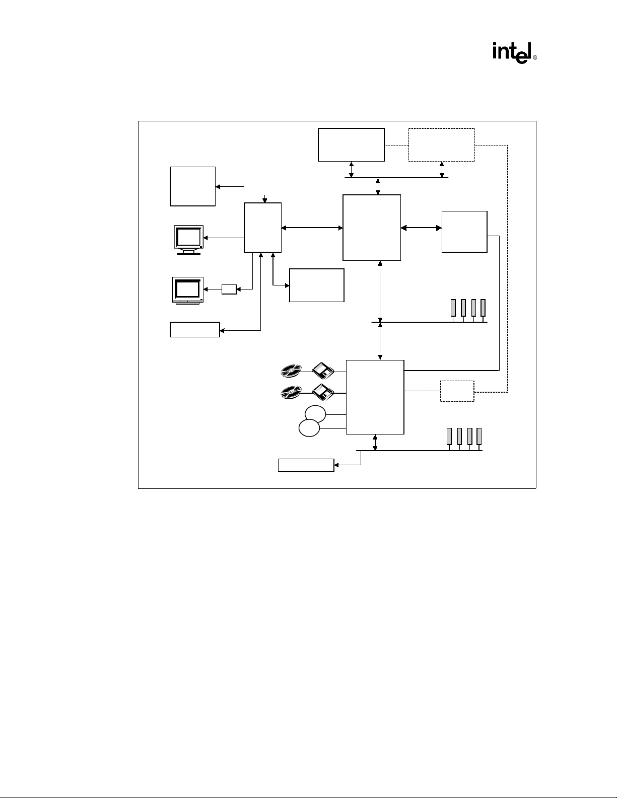
Architectural Overview
Figure 1-1. Intel
®
440BX AGPset System Block Diagram
Pentium®
Processor
Video
- DVD
- Camera
- VCR
Display
TV
Video BIOS
- VMI
- Video Capture
Graphics
Encoder
2 IDE Ports
(Ultra DMA/33)
Device
2 USB
Ports
2X AGP Bus
Graphics
Local Memory
USB
USB
II
Host Bus
82443BX
Host Bridge
82371EB
(PIIX4E)
(PCI-to-ISA
Bridge)
Pentium®
Processor
66/100
MHz
3.3V EDO &
SDRAM Support
Primary PCI Bus
(PCI Bus #0)
System MGMT (SM) Bus
II
Main
Memory
PCI Slots
IO
APIC
ISA Slots
ISA Bus
System BIOS
sys_blk.vsd
Host Interface
The Pentium II processor supports a second level cache via a back-side bus (BSB) interface. All
control for the L2 cache is handled by the processor. The 82443BX provides bus control signals
and address paths for transfers between the processors front-side bus (host bus), PCI bus, AGP and
main memory. The 82443BX supports a 4-deep in-order queue (i.e., supports pipelining of up to 4
outstanding transaction requests on the host bus). Due to the system concurrency requirements,
along with support for pipelining of address requests from the host bus, the 82443BX supports
request queuing for all three interfaces (Host, AGP and PCI).
Host-initiated I/O cycles are decoded to PCI, AGP or PCI configuration space. Host-initiated
memory cycles are decoded to PCI, AGP (prefetchable or non-prefetchable memory space) or
DRAM (including AGP aperture memory). For memory cycles (host, PCI or AGP initiated) that
target the AGP aperture space in DRAM, the 82443BX translates the address using the AGP
address translation table. Other host cycles forwarded to AGP are def ined by the A GP address map.
PCI and AGP initiated cycles that target the AGP graphics aperture are also translated using the
AGP aperture translation table. AGP-initiated cycles that target the AGP graphics aperture mapped
in main memory do not require a snoop cycle on the host bus, since the coherency of data for that
particular memory range will be maintained by the software.
1-2
82443BX Host Bridge Datasheet

Architectural Overview
DRAM Interface
The 82443BX integrates a DRAM controller that supports a 64-bit main memory interface. The
DRAM controller supports the following features:
DRAM type: Extended Data Out (EDO) (mobile only) or Synchronous (SDRAM) DRAM
•
controller optim ized for dual/qua d-bank SDRAM organi zation on a row by row basis
Memory Size: 8 MB to 512 MB (1GB with Registered DIMMs) with eight memory rows
•
Addressing Type: Symmetrical and Asymmetrical addressing
•
Memory Modules supported : Single and double density 3.3V DIMMs
•
DRAM device technology: 16 Mbit and 64 Mbit
•
DRAM Speeds: 60 ns for EDO and 100/66 MHz for synchronous memory (SDRAM).
•
The Intel
(SPD) mechanism using the SMBus interface. The 82443BX provides optional data integrity
features including ECC in the memory array. During reads from DRAM, the 82443BX provides
error checking and correction of the data. The 82443BX supports multiple-bit error detection and
single-bit error correction when ECC mode is enabled and single/multi-bit error detection when
correction is disabled. During writes to the DRAM, the 82443BX generates ECC for the data on a
QWord basis. Partial QWord writes require a read-modify-write cycle when ECC is enabled.
AGP Interfa ce
The 82443BX AGP implementation is compatible with the following:
•
•
The 82443BX supports only a synchronous AGP interface coupling to the 82443BX core
frequency. The AGP interface can reach a theoretical ~500 MByte/sec transfer rate (i.e., using
133 MHz AGP compliant dev ic es).
PCI Interface
The 82443BX PCI interface is 3.3V (5V tolerant), 33 MHz Rev. 2.1 compliant and supports up to
five extern al PCI bus masters in addition to the I/O bridge (PIIX4/PIIX4E). The PCI-to-DRAM
interface can reach over 100 MByte/sec transfer rate for streaming reads and over 120 MBytes/sec
for streaming writes.
System Clocking
®
440BX AGPset also pro vides DIMM plug-an d-pla y suppo rt via Serial Presence Detect
The Accelerated Graphics Port Specification, Rev 1.0
Accelerated Graphics Port Memory Performance Specification, Rev 1.0 (4/12/96)
The 82443BX operates the host interface at 66 or 100 MHz, the SDRAM/core at 66 or 100 MHz,
PCI at 33 MHz and AGP at 66/133 MHz.
I/O APIC
I/O APIC is used to support dual processors as well as enhanced interrupt processing in the single
processor environment. The 82443BX supports an external status output signal that can be used to
control synchronization of interru pts in configurations that use PIIX4E with stand-al on e I/O APIC
component.
82443BX Host Bridge Datasheet
1-3


Signal Description
Signal Description
This chapter provides a detailed description of 443BX signals. The signals are arranged in
functional groups according to their associated interface.
The “#” symbol at the end of a signal name indicates that the active, or asserted state occurs when
the signal is at a low voltage level. When “#” is not present after the signal name the signal is
asserted when at the high voltage level.
The following notations are used to describe the signal type:
I Input pin
O Output pin
OD Open Drain Output pin. This pin requires a pullup to the VCC of the processor core
I/OD Input / Open Drain Output pin. This pin requi res a pul lup t o the VCC o f the p rocesso r
core
I/O Bi-directional Input/Output pin
The signal description also includes the type of buffer used for the particular signal:
GTL+ Open Drain GTL+ interface signal. Refer to the GTL+ I/O Specification for complete
details
2
PCI PCI bus interface signals. These signals are compliant with the PCI 3.3V and 5.0V
Signaling Environment DC and AC Specifications
AGP AGP interface signals. These signals are compatible with AGP 3.3V Signaling
Environment DC and AC Specificati ons
CMOS The CMOS buffers are Low Voltage TTL compatible signals. These are 3.3V only.
2.1 Host Interface Signals
Table 2-1. Host Interface Signals (Sheet 1 of 2)
Name Type Description
CPURST#
A[31:3]#
HD[63:0]#
O
GTL+
I/O
GTL+
I/O
GTL+
CPU Reset.
generates this signal based on the PCIRST# input (from PIIX4E) and also the
SUSTAT # pin in mobile mode. The CPURST# allows the CPUs to begin execution in
a known state.
Address Bus:
A[31:3]# are inputs.
Host Data:
signals are inverted on the CPU bus.
The CPURST# pin is an output from the 82443BX. The 82443BX
A[31:3]# connect to the CPU address bus. During CPU cycles, the
These signals are connected to the CPU data bus. Note that the data
82443BX Host Bridge Datasheet
2-1
Signal Description
Table 2-1. Host Interface Signals (Sheet 2 of 2)
Name Type Description
I/O
ADS#
BNR#
BPRI#
BREQ0#
DBSY#
DEFER#
DRDY#
HIT#
HITM#
HLOCK#
HREQ[4:0]#
HTRDY#
RS[2:0]#
GTL+
GTL+
GTL+
GTL+
GTL+
GTL+
GTL+
GTL+
GTL+
GTL+
GTL+
GTL+
GTL+
Address Strobe:
cycles of a request phase.
I/O
Block Next Request:
new request. This signal is used to dynamically control the CPU bus pipeline depth.
Priority Agent Bus Request:
O
bus. It asserts this signal to obtain the ownership of the address bus. This signal has
priority over symmetric bus requests and will cause the current symmetric owner to
stop issuing new transactions unless the HLOCK# signal was asserted.
Symmetric Agent Bus Request:
O
asserted to configure the symmetric bus agents. BREQ0# is negated 2 host clocks
after CPURST# is negated.
I/O
Data Bus Busy:
requiring more than one cycle.
Defer:
O
I/O
I/O
I/O
I
I/O
I/O
I/O
The 82443BX generates a deferred response as defined by the rules of the
82443BX’s dynamic defer policy. The 82443BX also uses the DEFER# signal to
indicate a CPU retry response.
Data Ready:
Hit:
Indicates that a caching agent holds an unmodified version of the requested line.
Also driven in conjunction with HITM# by the target to extend the snoop window.
Hit Modified:
requested line and that this agent assumes responsibility for providing the line. Also
driven in conjunction with HIT# to ex tend the snoop window.
Host Lock:
until the negation of HLOCK# must be atomic, i.e. no PCI or AGP snoopable access
to DRAM is allowed when HLOCK# is asserted by the CPU.
Request Command:
the signals define the transaction type to a level of detail that is sufficient to begin a
snoop request. In the second clock, the signals carry additional information to define
the complete transaction type. The transactions supported by the 82443BX Host
Bridge are defined in the Host Interface section of this document.
Host Target Ready:
the data transfer phase.
Response Signals:
RS[2:0] Response type
000 Idle state
001 Retry response
010 Deferred response
011 Reserved (not driven by 82443BX)
100 Hard F ailure (not driv en by 82443BX)
101 No data response
110 Implicit Writeback
111 Normal data response
The CPU bus owner asserts ADS# to indicate the first of two
Used to block the current request bus owner from issuing a
The 82443BX is the only Priority Agent on the CPU
Asserted by the 82443BX when CPURST# is
Used by the data bus owner to hold the data bus for transfers
Asserted for each cycle that data is transferred.
Indicates that a caching agent holds a modified version of the
All CPU bus cycles sampled with the assertion of HLOCK# and ADS#,
Asserted during both clocks of request phase. In the first clock,
Indicates that the target of the CPU transaction is able to enter
Indicates type of response according to the following the table:
2-2
NOTE:
1. All of the signals in the host interface are described in the CPU External Bus Specification. The preceding
table highlights 82443BX specific uses of these signals.
82443BX Host Bridge Datasheet
Table 2-2 lists the CPU bus interface signals which are NOT supported by the Intel® 440BX
yp
p
AGPset.
Table 2-2. Host Signals Not supported by the 82443BX
Signal Function Not Supported By 82443BX
A[35:32]# Address Extended addressing (over 4 GB)
AERR# Address Parity Error Parity protection on address bus
AP[1:0]# Address Parity Parity protection on address bus
BINIT# Bus Initialization Checking for bus protocol violation and protocol recovery mechanism
DEP[7:0]# Data Bus ECC/Parity Enhanced data bus integrity
IERR# Internal Error Direct internal error observation via IERR# pin
INIT# Soft Reset Implemented by PIIX4E, BIST supported by external logic.
BERR# Bus Error Unrecoverable error without a bus protocol violation
RP# Request Parity Parity protection on ADS# and PREQ[4:0]#
RSP#
Response Parity
Signal
Parity protection on RS[2:0]#
Signal Description
2.2 DRAM Interface
Table 2-3.
DRAM Interface
Name T
RASA[5:0]#
/CSA[5:0]#
RASB[5:0]#
/CSB[5:0]#
CKE[3:2]
/CSA[7:6]#
CKE[5:4]
/CSB[7:6]#
CASA[7:0]#
/DQMA[7:0]
CASB[1,5]#
/DQMB[1,5]
Signals (Sheet 1 of 2)
e
Row Address Strobe (EDO):
the MAxx lines into the DRAMs. Each signal is used to select one DRAM row.
These signals drive the DRAM array directly without any external buffers.
O
Chip Select (SDRAM):
CMOS
CMOS
CMOS
CMOS
perform the function of selecting the particular SDRAM components during the
active state.
Note that there are 2 copies of RAS# per physical memory row to improve the
loading.
Clock Enable:
refresh or power-down command to an SDRAM array when entering system
suspend. CKE is also used to dynamically power down inactive SDRAM rows.
This CKE function is not supported with Registered DIMMs.
O
Chip Select (SDRAM):
particular SDRAM components during the active state.
Note that there are 2 copies of CS# per physical memory row to reduce the
loading.
Column Address Strobe A-side (EDO):
latch the column address on the MA[13:0] lines into the DRAMs of the A half of
the memory array . These are activ e low signals that drive the DRAM array directly
O
without external buffering.
Input/Output Data Mask A-side (SDRAM):
memory array and act as synchronized output enables during read cycles and as
a byte enables during write cycles.
Column Address Strobe B-side (EDO) / Input/Output Data Mask B-side
O
(SDRAM):
signals are used to reduce the loading in an ECC configuration
Descri
These signals are used to latch the row address on
For the memory row configured with SDRAM these pins
In mobile mode, SDRAM Clock Enable is used to signal a self-
These pins perform the function of selecting the
The same function as a corresponding signals for A side. These
tion
The CASA[7:0]# signals are used to
These pins control A half of the
82443BX Host Bridge Datasheet
2-3

Signal Description
y
Table 2-3.
DRAM Interface
Name T
GCKE/CKE1
SRAS[B,A]#
CKE0/FENA
SCAS[B,A]#
MAA[13:0]
MAB[12:11]#
MAB[13,10]
MAB[9:0]#
WEA#
WEB#
MD [63:0]
MECC[7:0]
Signals (Sheet 2 of 2)
pe
Global CKE (SDRAM):
power down mode for the SDRAM. External logic must be used to implement this
function.
SDRAM Clock Enable (CKE1):
O
signal a self-refresh or power-down command to an SDRAM array when entering
CMOS
CMOS
CMOS
CMOS
CMOS
CMOS
I/O
CMOS
I/O
CMOS
system suspend. CKE is also used to dynamically power down inactive SDRAM
rows. The combination of SDRAMPWR (SDRAM register) and MMCONFIG
(DRAMC register) determine the functioning of the CKE signals. Refer to the
DRAMC register (Section 3.3.15, “DRAMC—DRA M Control Register (Device 0)”
on page 3-19) for more details.
SDRAM Row Address Strobe (SDRAM):
O
copies of the same logical SRASx signal (for loading purposes) used to generate
SDRAM command encoded on SRASx/SCASx/WE signals.
SDRAM Clock Enable 0 (CKE0).
is used to signal a self-refresh or power-down command to an SDRAM array
when entering system suspend. CKE is also used to dynamically power down
O
inactive SDRAM rows.
FET Enable (FENA):
proper MD path through the FET switches (refer to Section4.3, “DRAM Interface”
on page 4-14 for more details).
SDRAM Column Address Strobe (SDRAM):
O
multiple copies of the same logical SCASx signal (for loading purposes) used to
generate SDRAM command encoded on SRASx/SCASx/WE signals.
Memory Address(EDO/SDRAM):
provide the multiplexed row and column address to DRAM. There are two sets of
O
MA signals which drive a max. of 2 DIMMs each. MAA[12:11,9:0] are inverted
copies of MAB[12:11,9:0]#. MAA[13,10] and MAB[13,10] are identical copies.
Each MAA/MAB[13:0] line has a programmable buffer strength to optimize for
different signal loading conditions.
Write Enable Signal (EDO/SDRAM):
O
The WE# lines have a programmable buffer strength to optimize for different
signal loading conditions.
Memory Data (EDO/SDRAM):
data bus.
Memory ECC Data (EDO/SDRAM):
during access to DRAM.
Description
Global CKE is used in a 4 DIMM configuration requiring
In mobile mode, SDRAM Clock Enable is used to
The SRAS[B,A]# signals are multiple
In mobile mode, CKE0 SDRAM Clock Enable
In a 4 DIMM configuration. FENA is used to select the
The SCAS[B,A]# signals are
MAA[13:0] and MAB[13:0]# are used to
WE# is asserted during writes to DRAM.
These signals are used to interface to the DRAM
These signals carry Memory ECC data
2-4
82443BX Host Bridge Datasheet

2.3 PCI Interface (Primary)
Table 2-4. Primary PCI Interface Signals (Sheet 1 of 2)
Name Type Description
AD[31:0]
DEVSEL#
FRAME#
IRDY#
C/BE[3:0]#
PAR
PLOCK#
TRDY#
PCI Address/Data:
Address is driven by the 82443BX with FRAME# assertion, data is driven or received
I/O
in the following clocks. When the 82443BX acts as a target on the PCI Bus, the
PCI
AD[31:0] signals are inputs and contain the address during the first clock of FRAME#
assertion and input data (writes) or output data (reads) on subsequent clocks.
Device Select:
decoded its address as the target of the current access. The 82443BX asserts
I/O
DEVSEL# based on the DRAM address range or
PCI
by a PCI initiator. As an input it indicates whether any device on the bus has been
selected.
Frame:
FRAME# is an output when the 82443BX acts as an initiator on the PCI Bus.
FRAME# is asserted by the 82443BX to indicate the beginning and duration of an
access. The 82443BX asserts FRAME# to indicate a bus transaction is beginning.
I/O
While FRAME# is asserted, data transfers continue. When FRAME# is negated, the
PCI
transaction is in the final data phase. FRAME# is an input when the 82443BX acts as
a PCI target. As a PCI target, the 82443BX latches the C/BE[3:0]# and the AD[31:0]
signals on the first clock edge on which it samples FRAME# active.
Initiator Ready:
I/O
input when the 82443BX acts as a PCI target. The assertion of IRDY# indicates the
current PCI Bus initiator's ability to complete the current data phase of the
PCI
transaction.
Command/Byte Enable:
multiplexed on the same pins. During the address phase of a transaction, C/BE[3:0]#
define the bus command. During the data phase C/BE[3:0]# are used as byte
enables. The byte enables determine which byte lanes carry meaningful data. PCI
Bus command encoding and types are listed below.
C/BE[3:0]# Command Type
0000 Interrupt Acknowledge
0001 Special Cycle
0010 I/O Read
0011 I/O Write
I/O
0100 Reserved
PCI
0101 Reserved
0110 Memory Read
0111 Memory Write
1000 Reserved
1001 Reserved
1010 Configuration Read
1011 Configuration Write
1100 Memory Read Multiple
1101 Reserved (Dual Address Cycle)
1110 Memory Read Line
1111 Memory Write and Invalidate
Parity:
I/O
PCI
I/O
PCI
I/O
PCI
PAR is driven by the 82443BX when it acts as a PCI initiator during address
and data phases for a write cycle, and during the address phase for a read cycle. PAR
is driven by the 82443BX when it acts as a PCI target during each data phase of a
PCI memory read cycle. Even parity is generated across AD[31:0] and C/BE[3:0]#.
Lock:
PLOCK# indicates an exclusive bus operation and may require multiple
transactions to complete. When PLOCK# is asserted, non-exclusive transactions may
proceed. The 82443BX supports lock for CPU initiated cycles only. PCI initiated
locked cycles are not supported.
Target Ready:
output when the 82443BX acts as a PCI target. The assertion of TRDY# indicates the
target agent's ability to complete the current data phase of the transaction.
These signals are connected to the PCI address/data bus.
Device select, when asserted, indicates that a PCI target device has
IRDY# is an output when 82443BX acts as a PCI initiator and an
TRDY# is an input when the 82443BX acts as a PCI initiator and an
Signal Description
AGP address range
PCI Bus Command and Byte Enable signals are
being accessed
82443BX Host Bridge Datasheet
2-5

Signal Description
y
Table 2-4. Primary PCI Interface Signals (Sheet 2 of 2)
Name Type Description
System Error:
SERR# assertion by the 82443BX is enabled globally via SERRE bit of the PCICMD
register. SERR# is asserted under the following conditions:
In an ECC configuration, the 82443BX asserts SERR#, for single bit (correctable)
ECC errors or multiple bit (non-correctable) ECC errors if SERR# signaling is enabled
via the ERRCMD control register. Any ECC errors received during initialization should
be ignored.
• The 82443BX asserts SERR# for one clock when it detects a target abort during
82443BX initiated PCI cycle.
• The 82443BX can also assert SERR# when a PCI parity error occurs during the
SERR#
STOP#
NOTE:
1. All PCI interface signals conform to the PCI Rev 2.1 specification.
I/O
PCI
I/O
PCI
address or data phase.
• The 82443BX can assert SERR# when it detects a PCI address or data parity
error on AGP.
• The 82443BX can assert SERR# upon detection of access to an invalid entry in
the Graphics Aperture Translation Table.
• The 82443BX can assert SERR# upon detecting an invalid AGP master access
outside of AGP aperture and outside of main DRAM range (i.e. in the 640k - 1M
range or above TOM).
• The 82443BX can assert SERR# upon detecting an invalid AGP master access
outside of AGP aperture.
• The 82443BX asserts SERR# for one clock when it detects a target abort during
82443BX initiated AGP cycle.
Stop:
STOP# is an input when the 82443BX acts as a PCI initiator and an output
when the 82443BX acts as a PCI target. STOP# is used for disconnect, retry, and
abort sequences on the PCI Bus.
The 82443BX asserts this signal to indicate an error condition. The
2.4 Primary PCI Sideband Interface
Table 2-5.
Primar
PHOLD#
PHLDA#
WSC#
PREQ[4:0]#
PGNT[4:0]#
PCI Sideband Interface
Name Type Description
PCI Hold:
ownership. The 82443BX will flush and disable the CPU-to-PCI write buffers before
I
granting the PIIX4E the PCI bus via PHLDA #. This prevents bus deadlock between
PCI
PCI and ISA.
PCI Hold Acknowledge:
O
ownership to the PIIX4E after CPU-PCI post buffers have been flushed and disabled.
PCI
Write Snoop Complete.
O
CMOS
snoop activity on the CPU bus on the behalf of the last PCI-DRAM write transaction is
complete and that is safe to send the APIC interrupt message.
PCI Bus Request:
I
internal PCI arbiter.
PCI
PCI Grant: P
O
PCI arbiter.
PCI
Signals
This signal comes from the PIIX4E. It is the PIIX4E request for PCI bus
This signal is driven by the 82443BX to grant PCI bus
This signal is asserted active to indicate that all that the
PREQ[4:0]# are the PCI bus request signals used as inputs by the
GNT[4:0]# are the PCI bus grant output si gnals generated b y the internal
2-6
82443BX Host Bridge Datasheet

2.5 AGP Interface Signals
q
g
q
y
]
g
y q
[
]
There are 17 new signals added to the normal PCI group of signals that together constitute the AGP
interface. The sections below describe their operation and use, and are organized in five groups:
AGP Addressing Signals
•
AGP Flow Control Signals
•
AGP Status Signals
•
AGP Clocking Signals - Strobes
•
PCI Signals
•
Table 2-6. AGP Interface Signals (Sheet 1 of 2)
Name Type Description
AGP Sideband Addressing Signals
PIPE#
SBA[7:0]
RBF#
ST[2:0]
Pipelined Read:
address is to be
I
clock ed
queued across the AD bus.
AGP
(graphics controller)
may not use PIPE#.
Sideband Address:
I
command to the 82443BX from the AGP master. Note that, when sideband
addressing is disabled, these signals are isolated (no external/internal pull-ups are
AGP
required).
Read Buffer Full.
re
I
AGP
O
AGP
uested low priority read data. When RBF#
to return low priority read data to the AGP master on the first block. RBF# is only
sampled at the beginning of a cycle.
If the AGP master is always ready to accept return read data then it is not required to
implement this signal.
Status
Bus:
it ma
do. ST[2:0
When G
GNT#
000 Indicates that previously requested low priority read data is being returned to
the master.
001 Indicates that previously requested high priority read data is being returned to
the master.
010 Indicates that the master is to provide low priority write data for a previously
queued write command.
011 Indicates that the master is to provide high priority write data for a previously
queued write command.
100 Reserved
101 Reserved
110 Reserved
111 Indicates that the master has been
The master ma
transaction by asserting
82443BX and an input to the master.
This signal is asserted by the current master to indicate a full width
ueued by the target. The master queues one request each rising
e while PIPE#
AGP Flow Control Signals
This bus provides information from the arbiter to a AGP Master on what
only have meaning to the master when its G
is deasserted these signals have no meaning and must be ignored.
Signal Description
1
is asserted. When
and is an input to the 82443BX. Note that initial AGP designs
This bus
This signal indicates if the master is ready to accept previously
AGP Status Signals
ueue AGP requests by asserting PIPE#
is a sustained tri-state signal from
PIPE#
provides an additional bus to pass address and
FRAME#. ST
is deasserted no new requests are
PIPE#
is asserted the 82443BX is not allowed
iven permission to start a bus transaction.
are always an output from the
2:0
masters
is asserted.
GNT#
or start a PCI
82443BX Host Bridge Datasheet
2-7
Signal Description
g
y
g
g
g
[
]
g
(
g
Table 2-6. AGP Interface Signals (Sheet 2 of 2)
Name Type Description
AD Bus Strobe A:
ADSTB_A
ADSTB_B
SBSTB
GFRAME#
GIRDY#
GTRDY#
GSTOP#
GDEVSEL#
GREQ#
GGNT#
GAD[31:0]
GC/BE[3:0]#
GPAR
I/O
The agent that is providing data drives this signal. This signal requires an 8.2K ohm
AGP
external pull-up resistor.
I/O
AD Bus Strobe B:
signal requires an 8.2K ohm external pull-up resistor.
AGP
I
Sideband Strobe:
requires an 8.2K ohm external pull-up resistor.
AGP
AGP FRAME# Protocol SIgnals (similar to PCI)
I/O
Graphics Frame:
by its own pull up resistor.
AGP
Graphics Initiator Ready:
master is ready to provide
asserted for a write operation, the master is not allowed to insert wait states. The
assertion of IRDY# for reads indicates that the master is ready to transfer to a
I/O
subsequent block (32 bytes) of read data. The master is
AGP
states during the initial data transfer (32 bytes) of a read transaction. However, it may
insert wait states after each 32 byte block is transferred.
(There is no GFRAME#
Graphics Target Ready:
target is ready to provide read data for the entire transaction (when the tr ansfer siz e is
I/O
less than or equal to 32 bytes) or is ready to transfer the initial or subsequent block
(32 bytes) of data when the transfer size is greater than 32 bytes. The target is
AGP
allowed to insert wait states after each block (32 bytes) is transferred on both read
and write transactions.
I/O
Graphics Stop:
AGP
I/O
Graphics Device Select:
AGP
I
Graphics Request:
PCI or AGP request.)
AGP
Graphics Grant:
. The additional information indicates that the selected master is the recipient
ST
O
AGP
I/O
AGP
I/O
AGP
I/O
AGP
2:0
of previously requested read data (high or normal priority), it is to provide write data
(high or normal priority), for a previously queued write command or has been given
permission to start a bus transaction (AGP or PCI).
Graphics Address/Data:
Graphics Command/Byte Enables:
information
usin
PIPE#
not used during the return of read data.
Graphics Parity:
transactions as defined by the PCI specification.
AGP Clocking Signals - Strobes
This si
nal provides timing for double clocked data on the AD
This signal is an additional copy of the AD_STBA signal. This
THis signal provides timing for a side-band bus. This signal
2
Same as PCI. Not used b
New meanin
all
write data for the current transaction. Once IRDY# is
--
GIRDY#
New meanin
Same as PCI. Not used by AGP.
Same as PCI. Not used by AGP.
Same as PCI. (Used to request access to the bus to initiate a
Same meanin
Same as PCI.
different commands than PCI) when requests are being queued when
. Provide valid byte information during AGP write transactions and are
Same as PCI. Not used on AGP transactions, but used during PCI
relationship for AGP transactions.)
as PCI but additional information is provided on
AGP. GFRAME#
. GIRDY#
. GTRDY#
Sli
htly different meaning. Provides command
indicates the AGP compliant
indicates the AGP compliant
remains deasserted
never
allowed to insert wait
bus.
NOTE:
1.
AGP Sideband Addressing Signals.
the AGP master. Note that the master can only use one mechanism. When PIPE# is used to queue
addresses the master is not allowed to queue addresses using the SBA bus. For ex ample, during
configuration time, if the master indicates that it can use either mechanism, the configuration software will
indicate which mechanism the master will use. Once this choice has been made, the master will continue to
use the mechanism selected until the master is reset (and reprogrammed) to use the other mode. This
change of modes is not a dynamic mechanism but rather a static decision when the device is first being
configured after reset.
2-8
The above table contains two mechanisms to queue requests by
82443BX Host Bridge Datasheet

2. PCI signals are redefined when used in AGP transactions carried using AG P protocol extension. For
transactions on the AGP interface carried using PCI protocol these signals completely preserve PCI
semantics. The exact role of all PCI signals during AGP transactions is in Table 2-6.
3. The LOCK# signal is not supported on the AGP interface (even for PCI operations).
4. PCI signals described in Table 2-4 behave according to PCI 2.1 specifications when used to perform PCI
transactions on the AGP Interface.
2.6 Clocks, Reset, and Miscellaneous
Table 2-7. Clocks, Reset, and Miscellaneous
Name Type Description
HCLKIN
PCLKIN
DCLKO
DCLKWR
PCIRST#
GCLKIN
GCLKO
CRESET#
TESTIN#
I
CMOS
I
CMOS
O
CMOS
I
CMOS
I
CMOS
I
CMOS
O
CMOS
O
CMOS
I
CMOS
Host Clock In:
82443BX logic that is in the Host clock domain.
When SUSTAT# is active, there is an internal 100K ohm pull down on this signal.
PCI Clock In:
an external clock synthesizer component from the host clock. This clock is used by all
of the 82443BX logic that is in the PCI clock domain.
When SUSTAT# is active, there is an internal 100K ohm pull down on this signal.
SDRAM Clock Out:
buffer clock device that produces multiple copies for the DIMMs.
SDRAM Write Clock:
This clock is used by the 82443BX when writing data to the SDRAM array.
Note: See the Design Guide for routing constraints.
PCI Reset:
and bi-directional signals will also tri-state compliant to PCI Rev 2.0 and 2.1
specifications.
When SUSTAT# is active, there is an internal 100K ohm pull down on this signal.
AGP Clock In:
AGP Clock Out:
both the reference input pin on the 82443BX and the AGP compliant device.
Delayed CPU Reset:
to control the multiplexer for the CPU strap signals. CRESET# is delayed from
CPURST# by two host clocks.
Note:
This pin requires an external pull-up resistor. If not used, no pull up is required.
Test Input:
Note: This pin has an internal 50K ohm pull-up.
This pin receives a buffered host clock. This clock is used by all of the
This is a buffered PCI clock reference that is synchronously derived by
66 or 100 MHz SDRAM clock reference. It feeds an external
Feedback reference from the external SDRAM clock buffer.
When asserted, this signal will reset the 82443BX logic. All PCI output
The GCLKIN input is a feedback reference from the GCLKOUT signal.
The frequency is 66 MHz. The GCLKOUT output is used to feed
CRESET# is a delayed copy of CPURST#. This signal is used
This pin is used for manufa cturing, and board level test purposes.
Signal Description
Table 2-8. Power Management Interface
Name Type Description
Primary PCI Clock Run:
or maintain the PCI clock by the assertion of CLKRUN#. The 82443BX tristates
I/OD
CLKRUN#
SUSTAT#
BXPWROK
CMOS
CMOS
CMOS
82443BX Host Bridge Datasheet
CLKRUN# upon deassertion of PCIRST# (since CLK is running upon deassertion of
reset). If connected to PIIX4E an external 2.7K Ohm pull-up is required for Desktop,
Mobile requires (8.2k–10K) pull-up. Otherwise, a 100 Ohm pull down is required.
Suspend Status (from PIIX):
I
from the PIIX4E. It is used to isolate the suspend voltage well and enter/exit DRAM
self-refresh mode. During POS/STR SUSTAT# is active.
I
BX Power OK:
indicates valid power is applied to the 82443BX.
The 82443BX requests the central resource (PIIX4E) to start
SUSTAT# signals the system suspend state transition
BXPWROK input must be connected to the PWROK signal that
2-9
Signal Description
Table 2-9. Reference Pins
Name Description
GTLREF[B:A] GTL Buffer voltage reference input
VTT[B:A] GTL Threshold voltage for early clamps
VCC Power pin @ 3.3V
VSS Ground
REF5V PCI 5V reference voltage (for 5V tolerant buffers)
AGPREF Ex ternal Input Reference
2.7 Power-Up/Reset Strap Options
Ta ble 2-10 is the list of all power-up options that are loaded into the 82443BX during cold reset.
The 82443BX is required to float all the signals connected to straps during cold reset and keep
them floated for a minimum of 4 host clocks after the end of cold reset sequence. Cold reset
sequence is performed when the 82443BX power is applied.
Note: All signals used to select power-up strap options are connected to either internal pull-down or pull-
up resistors of minimum 50K ohm s (max im um i s 150 K). That sel ect s a def ault mode on the signal
during reset. To enable different mod es, e xternal pul l ups or pul l do wns (the op posite of the i nternal
resistor) of approximately 10K ohm can be connected to particular signals. These pull up or pull
down resistors should be connected to the 3.3V power supply.
During normal operation of the 82443BX, including while it is in suspend mode, the paths from
GND or Vcc to internal strapping resistors are disabled to effectively disable the resistors. In these
cases, the MAB# lines are driven by the 82443BX to a valid voltage levels.
Note: Note that when resuming from suspend, even while PCIRST# is active, the MAB# lines remain
driven by the 82443BX and the strapping latches maintain the value stored during the cold reset.
This first column in Table 2-10 lists the sign al that is sampled to obtain the strapping option. The
second column shows which register the strapping option is loaded into. The third column is a
description of what functionality the strapping selects.
The GTL+ signals are connected to the VTT through the normal pull-ups. CPU bus straps
controlled by the 82443BX (e.g. A7# and A15#), are driven active at least six clocks prior to the
active-to-inactive edge of CPURST# and driven inactive four clocks after the active-to-inactive
edge of the CPURST#.
2-10
82443BX Host Bridge Datasheet

Table 2-10. Strapping Options
Signal Description
Signal
MAB13#
MAB12# NBXCFG[13]
MAB11# NBXCFG[2]
MAB10 PMCR[3]
MAB9# PMCR [1]
MAB8#
MAB7# DRAMC[5]
MAB6# none
A[15]# none
A7# none
Register
Name[bit]
Description
Reserved.
Host Frequency Select:
66 MHz. If MAB#12 is strapped to 1, the host bus frequency is 100 MHz. An
internal pull-down is used to provide the default setting of 66 MHz.
In-Order Queue Depth Enable.
of PCIRST#, then the 82442BX will drive A7# low during the CPURST#
deassertion. This forces the CPU bus to be configured for non-pipelined operation.
If MAB11 is strapped to 1 (default), then the 82443BX does not drive the A7# low
during reset, and A7# is sampled in default non-driven state (i.e. pulled-up as far as
GTL+ termination is concerned) then the maximum allowable queue depth by the
CPU bus protocol is selected (i.e., 8).
Note that internal pull-up is used to provide pipelined bus mode as a default.
Quick Start Select.
mode is used.
MAB10 = 0 (default) for normal stop clock mode. If MAB10 = 1 during the rising
edge of PCIRST#, then the 82443BX will drive A15# low during CPURST#
deassertion. This will configure the CPU for Quick Start mode of operation.
Note that internal pull-down is used to provide normal stop clock mode as a default.
AGP Disable:
are tri-stated and isolated. When strapped to a 0 (default), the AGP interface is
enabled.
When MMCONFIG is strapped active, we require that AGP_DISABLE is also
strapped active. When MMCONFIG is strapped inactive, AGP_DISABLE can be
strapped active or inactive but IDSEL_REDIRECT (bit 16 in NBXCFG register)
must never be activated.
This signal has an internal pull-down resistor.
Reserved.
Memory Module Configuration, MMCONFIG:
82443BX configures its DRAM interface in a 430-TX compatible manner. These
unused inputs are isolated while unused outputs are tri-stated: RASB[5:0]#/
CSB[5:0]#, CKE[3:2]/CSA[7:6]#, CKE[5:4]/CSB[7:6]#, CASB[5,1]#/DQMB[5,1],
GCKE/CKE1, MAA[13:0], DCLKO.
When strapped to a 0 (default), the 82443BX DRAM signal are used normally.
IDSEL_REDIRECT (bit 16 in NBXCFG register) is programmed by BIOS, before it
begins with device enumeration process. The combination of SDRAMPWR
(SDRAMC register) and MMCONFIG (DRAMC register) determine the functioning
of the CKE signals. Refer to the DRAMC register for more details.
Note that internal pull-down is used to set the DRAM interface to a nor mal
configuration, as a default.
Host Bus Buffer Mode Select:
100 MHz host bus buffers are used (default).
When strapped ‘1’, the mobile Low Power GTL+ 66 MHz host bus buffers are
selected.
Note that internal pull-down is used to set the host bus buffers to a desktop
configuration as a default. External pull-up therefore is needed f or mobile systems,
only.
Quick Start Select.
will reflect if the quick start/stop clock mode is enabled in the processors.
In-order Queue Depth Status.
CPURST# reflects if the IOQD is set to 1 or maximum allowab le by the CPU bus.
When strapped to a 1, the AGP interface is disabled, all A GP signals
If MAB#12 is strapped to 0, the host bus frequency is 60/
If MAB11# is strapped to 0 during the rising edge
The value on this pin at reset determines which stop clock
When strapped to a 1, the
When strapped 0, the desktop GTL+ 66 MHz or
The value on A15# sampled at the rising edge of CPURST#
The value on A[7]# sampled at the rising edge of
NOTE:
1. Proper strapping must be used to define logical values for these signals. Default value “0”, or “1” provided by
the internal pull-up or pull-down resistor can be overridden by the external pull-up, or pull-down resistor
82443BX Host Bridge Datasheet
.
2-11


Register Description
Register Description
The 82443BX contains two sets of software accessible registers, accessed via the Host CPU I/O
address space:
1. Control re gisters that are I/O mapped into the CPU I/O space. These re gisters co ntrol access to
PCI and AGP configuration space.
2. Internal configuration registers residing within the 82443BX, partitione d into two logical
device register sets (“logical” since they reside within a single physical device). The first
register set is dedicated to Host-to-PCI Bridge functionality. This set (device 0) controls PCI
interface operations, DRAM configuration, and other chip-set operating parameters and
optional features. The second register set (dev ice 1) is dedicated to Host-to-AGP Bridge
functions (controls AGP interface configurations and operating parameters).
The following nomenclature is used for register access attributes.
RO Read Only. If a register is read only, writes to this register have no effect.
R/W Read/Write. A register with this attribute can be read and written
R/WC Read/Write Clear. A register bit with this attribute can be read and written.
However, a write of a 1 clears (sets to 0) the corresponding bit and a write of a 0 has
no effect.
R/WO Read/Write Once. A register bit with this attribute can be written to only once after
power up. After the first write, the bit becomes read only.
R/WL Read/Write/Lock. This register includes a lock bit. Once the lock bit has been set to
1, the register becomes read only.
3
The 82443BX supports PCI configuration space access using the mechanism denoted as
Configuration Mechanism #1 in the PCI specification.
The 82443BX internal registers (both I/O Mapped and Configuration registers) are accessible by
the Host CPU. The registers can be accessed as Byte, Word (16-bit), or DWord (32-bit) quantities,
with the exception of CONFADD which can on ly be accessed as a Dword. All multi-byte numeric
fields use "little-endian" ordering (i.e., lower addresses contain the least significant parts of the
field).
Some of the 82443BX registers described in this section contain reserved bits. These bits are
labeled "Reserved”. Software must deal correctly with fields that are reserved. On reads, software
must use appropriate masks to extract the defined bits and not rely on reserved bits being any
particular value. On writes, software must ensure that the values of reserved bit positions are
preserved. That is, the values of reserved bit positions must first be read, merged with the new
values for other bit positions and then written back.
Note: Software does not need to perform read, merge, write operation for the configuration address
register.
In addition to reserved bits within a register, the 82443BX contains address locations in the
configuration space of the Host-to-PCI Bridge entity that are marked either "Reserved" or “Intel
Reserved”. The 82443BX responds to accesses to “Reserved” address locations by completing the
host cycle. When a “Reserved” register location is read, a zero value is returned. (“Reserved”
registers can be 8-, 16-, or 32-bit in size). Writes to “Reserved” registers have no effect on the
82443BX Host Bridge Datasheet
3-1

Register Description
g
g
g
g
82443BX. Registers that are marked as “I ntel R eserv ed ” mu st not be modified b y system softw are.
Writes to “Intel Reserved” registers may cause system failure. Reads to “Intel Reserved” registers
may return a non-zero value. Software should not write to reserved configuration locations in the
device-specific region (above address offset 3Fh)
Upon reset, the 82443BX sets its internal configuration registers to predetermined default states.
However, there are a few exceptions to this rule.
1. When a reset occurs during the POS/STR state, several configuration bits are not reset to their
default state. These bits are noted in the following register description.
2. Some register values at reset are determined by external strapping options.
The default state represents the minimum functionalit y feature set requir ed to successfully bri ng up
the system. Hence, it does not represent the optimal system configuration. It is the responsibility of
the system initialization software (usually BIOS) to properly determine the DRAM configurations,
operating parameters and optional system features that are applicable, and to program the
82443BX registers accordingly.
3.1 I/O Mapped Registers
The 82443BX contains three registers that reside in the CPU I/O address space − the
Confi
uration Address (CONFADD) Register, the Configuration Data (CONFDATA)
Re
ister, and the Power Management Control Register. The Configuration Address
Re
ister enables/disables the configuration space and determines what portion of
confi
uration space is visible through the Configuration Data window.
3.1.1 CONFADD—Configuration Address Register
I/O Address: 0CF8h Accessed as a Dword
Default Value: 00000000h
Access: Read/Write
Size: 32 bits
CONFADD is a 32 bit register accessed only when referenced as a Dword. A Byte or Word
reference will "pass through" the Configuration Add ress Re g ister onto the PCI bus as an I/O cycle.
The CONFADD register contains the Bus Number, Device Number, Function Number, and
Register Number for which a subsequent configuration access is intended.
3-2
82443BX Host Bridge Datasheet
Bit Descriptions
Configuration Enable (CFGE).
31
enabled. If this bit is reset to 0 accesses to PCI configuration space are disabled.
30:24
23:16
15:11
10:8
7:2
1:0 Reserved.
Reserved.
Bus Number.
is either the 82443BX or the PCI Bus that is directly connected to the 82443BX, depending on the
Device Number field. A type 0 Configuration Cycle is generated on PCI if the Bus Number is
programmed to 00h and the 82443BX is not the target. If the Bus Number is non-zero a type 1
configuration cycle is generated on PCI or AGP with the Bus Number mapped to AD[23:16] during
the address phase.
Device Number.
a Type 1 Configuration cycle this field is mapped to AD[15:11]. During a Type 0 Configuration
Cycle this field is decoded and one bit among AD[31:11] is driven to a 1. The 82443BX is always
Device Number 0 for the Host-to-PCI bridge entity and Device Number 1 for the Host- AGP entity.
Therefore, the 82443BX internally references the AD11 and AD12 pins as corresponding IDSELs
for the respective devices dur ing PCI configuration cycles. NOTE: The AD11 and AD12 must not
be connected to any other PCI bus device as IDSEL signals.
Function Number.
the configuration registers of a particular function in a multi-function device to be accessed. The
82443BX only responds to configuration cycles with a function number of 000b; all other function
number values attempting access to the 82443BX (Device Number = 0 and 1, Bus Number = 0)
will generate a master abort.
Register Number.
specified by the other fields in the Configuration Address Register. This field is mapped to AD[7:2]
during PCI configuration cycles.
When the Bus Number is programmed to 00h the target of the Configuration Cycle
This field selects one agent on the PCI bus selected by the Bus Number. During
This field is mapped to AD[10:8] during PCIx configuration cycles. This allows
This field selects one register within a particular Bus, Device, and Function as
When this bit is set to 1 accesses to PCI configuration space are
Register Description
3.1.2 CONFDATA—Configuration Data Register
I/O Address: 0CFCh
Default Value: 00000000h
Access: Read/Write
Size: 32 bits
CONFDATA is a 32 bit read/write window into configuration space. The portion of configuration
space that is referenced by CONFDATA is determined by the contents of CONFADD.
Bit Descriptions
31:0
Configuration Data Windo w ( CDW).
CONFDATA I/O space will be mapped to configuration space using the contents of CONFADD.
If bit 31 of CONFADD is 1 any I/O reference that f alls i n the
82443BX Host Bridge Datasheet
3-3
Register Description
3.1.3 PM2_CTL—ACPI Power Control 2 Control Register
I/O Address: 0022h
Default Value: 00h
Access: Read/Write
Size: 8 bits
This register is used to disable both the PCI and AGP arbiters in the 82443BX to prevent any
external bus masters from acquiring the PCI or AGP bus. Any currently running PCI cycles will
terminate properly.
Accesses to this register are controlled by the Power Management Control Register (Offset 7Ah).
When bit 6 of the PMCR is set to ‘1 ’, the ACPI Register at I/O location 002 2h is enable d. When bi t
6 is set to ‘0’, I/O accesses to location 0022h are forwarded to PCI or AGP (if within programmable
IO range).
Bit Description
7:1 Reserved
Primary PCI and AGP Arbiter Request Disable (ARB_DIS).
82443BX will not respond to any PCI REQ# signals, AGP requests, or PHOLD# from PIIX4E going
active until this bit is set back to 0. Only External AGP and PCI requests are masked from the
0
arbiters. If the PIIX is in passiv e release mode, masking will not occur until an activ e release i s seen
via PHLDA# assertion. This prevents possible deadlock.
ARB_DIS has no effect on AGP side band signals or AGP data transfer requests.
When this bit is set to 1, the
3.2 PCI Configuration Space Access
The 82443BX implementation manifests two PCI devices within a single physical component
body:
Device 0 = Host-to-PCI Bridge = PCI bus #0 interface, Main Memory Controller, Graphics
•
Aperture controller, 82443BX specific AGP control registers.
Device 1 = Host-to-AGP interface = “Virtual” PCI-to-PCI Bridge, including AGP address
•
space mapping, normal PCI interface, and associated AGP sideband signal control.
Corresponding conf igu ration registers for both devices are mapped as de vices residi ng on PC I (b us
0). Configuration register layout and functionality for the Device #0 should be inspected carefully,
as new features added to the 82443BX initiated a reasonable level of change relative to other
proliferation’s of the Pentium
registers of the 82443BX Device # 1 are based on the normal conf igu ration space template of a PCIto-PCI Bridge as described in the PCI to PCI Bridge Architecture Specification.
Figure 3-1shows the PCI bus hierarchy for the 82443BX). In the PCI bus hierarchy, the primary
PCI bus is th e hi gh est level bus in the hiera rchy and is PCI b us #0 . Th e P CI- to -P CI bri d ge function
provides access to the AGP/PCI bus 0. This bus is below the primary bus in the PCI bus hierarchy
and is represented as PCI Bus #1.
®
Pro processor AGPsets (i.e. 440FX, 440LX). Configuration
3-4
82443BX Host Bridge Datasheet
 Loading...