


ST VIPer20, VIPer20SP, VIPer20DIP, VIPer20A, VIPer20ASP User Manual
...!
|
VIPer20/SP/DIP |
® |
VIPer20A/ASP/ADIP |
|
SMPS PRIMARY I.C. |
|
|
TYPE |
VDSS |
In |
RDS(on) |
VIPer20/SP/DIP |
620V |
0.5 A |
16 Ω |
VIPer20A/ASP/ADIP |
700V |
0.5 A |
18 Ω |
■ADJUSTABLE SWITCHING FREQUENCY UP TO 200 kHz
■CURRENT MODE CONTROL
■SOFT START AND SHUT DOWN CONTROL
■AUTOMATIC BURST MODE OPERATION IN STAND-BY CONDITION ABLE TO MEET “BLUE ANGEL” NORM (<1W TOTAL POWER CONSUMPTION)
■INTERNALLY TRIMMED ZENER REFERENCE
■UNDERVOLTAGE LOCK-OUT WITH HYSTERESIS
■INTEGRATED START-UP SUPPLY
■AVALANCHE RUGGED
■OVERTEMPERATURE PROTECTION
■LOW STAND-BY CURRENT
■ADJUSTABLE CURRENT LIMITATION
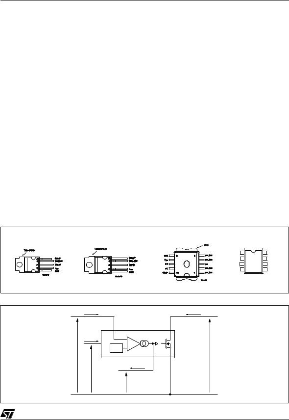
BLOCK DIAGRAM
PENTAWATT HV |
PENTAWATT HV (022Y) |
10 |
|
1 |
|
PowerSO-10™ |
DIP-8 |
DESCRIPTION
VIPer20/20A, made using VIPower M0 Technology, combines on the same silicon chip a state-of-the-art PWM circuit together with an optimized high voltage avalanche rugged Vertical Power MOSFET (620V or 700V / 0.5A).
Typical applications cover off line power supplies with a secondary power capability of 10W in wide range condition and 20W in single range or with doubler configuration. It is compatible from both primary or secondary regulation loop despite using around 50% less components when compared with a discrete solution. Burst mode operation is an additional feature of this device, offering the possibility to operate in stand-by mode without extra components.
|
OSC |
|
DRAIN |
|
|
|
|
||
|
|
|
|
|
|
|
ON/OFF |
|
|
|
|
|
|
|
|
|
|
|
|
|
|
|
|
|
OSCILLATOR |
|
|
|
|
|
||
|
|
|
SECURITY |
|
PWM |
|
|
|
|
|
|
||
|
|
|
LATCH |
|
LATCH |
|
|
|
|
|
|
||
|
UVLO |
|
|
|
|
S |
|
|
|
|
|
|
|
VDD |
R/S |
FF |
Q |
R1 |
FF |
Q |
|
|
|
|
|
||
LOGIC |
|
|
|
|
|
||||||||
|
|
|
|
|
|
|
|
|
|
|
|
||
|
|
|
|
S |
|
|
R2 R3 |
|
|
|
|
|
|
|
|
|
OVERTEMP. |
|
|
|
|
|
|
|
|
||
|
|
|
DETECTOR |
|
|
|
|
|
|
|
|
||
|
|
|
|
|
|
|
|
|
|
0.5V |
|
|
|
|
0.5 V |
+ |
|
1.7 |
|
|
|
|
+ |
+ |
_ |
6 V/A |
|
|
|
|
|
|
250 ns |
|
|
||||||
|
|
|
|
|
|
|
|
||||||
|
|
|
|
μs |
|
|
|
|
|
|
|
|
|
|
|
_ |
|
|
|
|
Blanking |
_ |
|
|
|
|
|
|
|
|
delay |
|
|
|
|
|
|
|
|||
|
|
|
|
|
|
|
|
|
|
|
|
|
|
|
ERROR |
|
|
|
|
|
|
|
|
|
|
CURRENT |
|
|
|
|
|
|
|
|
|
|
|
|
AMPLIFIER |
|
|
|
AMPLIFIER |
|
|
|
|
|
|
|
|
|
|
|
|
|
|
|
|
|
|
|
|
|
|
|
|
|
|
|
_ |
|
|
|
|
|
|
|
|
|
|
|
|
13 V |
+ |
|
|
|
|
|
|
|
|
|
|
|
|
|
|
4.5 V |
|
|
|
|
|
|
|
|
|
|
|
|
|
|
|
|
|
|
COMP |
|
|
|
|
SOURCE |
FC00491 |
|
|
|
|
|
|
|
|
|
|
|
|
||
July 2002 |
1/25 |
VIPer20/SP/DIP - VIPer20A/ASP/ADIP
ABSOLUTE MAXIMUM RATING
Symbol |
Parameter |
Value |
Unit |
|
|
|
|
|
Continuous Drain-Source Voltage (Tj=25 to 125°C) |
|
|
VDS |
for VIPer20/SP/DIP |
-0.3 to 620 |
V |
|
for VIPer20A/ASP/ADIP |
-0.3 to 700 |
V |
|
|
||
|
|
|
|
ID |
Maximum Current |
Internally limited |
A |
VDD |
Supply Voltage |
0 to 15 |
V |
VOSC |
Voltage Range Input |
0 to VDD |
V |
VCOMP |
Voltage Range Input |
0 to 5 |
V |
ICOMP |
Maximum Continuous Current |
± 2 |
mA |
Vesd |
Electrostatic Discharge (R =1.5kΩ; C=100pF) |
4000 |
V |
|
Avalanche Drain-Source Current, Repetitive or Not Repetitive |
|
|
ID(AR) |
(TC=100°C; Pulse width limited by T j max; δ < 1%) |
0.5 |
A |
for VIPer20/SP/DIP |
|||
|
for VIPer20A/ASP/ADIP |
0.4 |
A |
|
|
|
|
Ptot |
Power Dissipation at Tc=25ºC |
57 |
W |
Tj |
Junction Operating Temperature |
Internally limited |
°C |
Tstg |
Storage Temperature |
-65 to 150 |
°C |
THERMAL DATA
Symbol |
Parameter |
|
PENTAWATT |
PowerSO-10™ (*) |
DIP-8 |
Unit |
|
|
|
|
|
|
|
Rthj-pin |
Thermal Resistance Junction-pin |
Max |
|
|
20 |
°C/W |
Rthj-case |
Thermal Resistance Junction-case |
Max |
2.0 |
2.0 |
|
°C/W |
Rthj-amb. |
Thermal Resistance Ambient-case |
Max |
70 |
60 |
35 (#) |
°C/W |
(*) When mounted using the minimum recommended pad size on FR-4 board. |
|
|
|
|||
(#) On multylayer PCB. |
|
|
|
|
|
|
CONNECTION DIAGRAMS (Top View) |
|
|
|
|
|
|
PENTAWATT HV |
PENTAWATT HV (022Y) |
PowerSO-10™ |
|
DIP-8 |
|
|
|
OSC |
1 |
8 |
DRAIN |
|
|
Vdd |
|
|
DRAIN |
|
|
SOURCE |
|
|
DRAIN |
|
|
COMP |
4 |
5 |
DRAIN |
|
|
|
|
SC10540 |
|
CURRENT AND VOLTAGE CONVENTIONS
IDD |
|
ID |
VDD |
DRAIN |
|
IOSC |
- |
|
OSC |
+ |
|
13V |
|
|
VDD |
COMP SOURCE |
VDS |
|
|
|
|
ICOMP |
|
VOSC |
|
|
|
VCOMP |
|
|
|
FC00020 |
|
|
2/25 |

VIPer20/SP/DIP - VIPer20A/ASP/ADIP
ORDERING NUMBERS
PENTAWATT HV |
PENTAWATT HV (022Y) |
PowerSO-10™ |
DIP-8 |
|
|
|
|
VIPer20 |
VIPer20 (022Y) |
VIPer20SP |
VIPer20DIP |
|
|
|
|
VIPer20A |
VIPer20A (022Y) |
VIPer20ASP |
VIPer20ADIP |
|
|
|
|
PINS FUNCTIONAL DESCRIPTION
DRAIN PIN:
Integrated Power MOSFET drain pin. It provides internal bias current during start-up via an integrated high voltage current source which is switched off during normal operation. The device is able to handle an unclamped current during its normal operation, assuring self protection against voltage surges, PCB stray inductance, and allowing a snubberless operation for low output power.
SOURCE Pin:
Power MOSFET source pin. Primary side circuit common ground connection.
VDD Pin:
This pin provides two functions:
-It corresponds to the low voltage supply of the
control part of the circuit. If VDD goes below 8V, the start-up current source is activated and the output power MOSFET is switched off until the
VDD voltage reaches 11V. During this phase, the internal current consumption is reduced,
the VDD pin sources a current of about 2mA and the COMP pin is shorted to ground. After that, the current source is shut down, and the device tries to start up by switching again.
-This pin is also connected to the error amplifier, in order to allow primary as well as secondary regulation configurations. In case of primary regulation, an internal 13V trimmed reference
voltage is used to maintain VDD at 13V. For secondary regulation, a voltage between 8.5V
and 12.5V will be put on VDD pin by transformer design, in order to stick the output of the transconductance amplifier to the high state. The COMP pin behaves as a constant current
source, and can easily be connected to the output of an optocoupler. Note that any overvoltage due to regulation loop failure is still detected by the error amplifier through the VDD voltage, which cannot overpass 13V. The output voltage will be somewhat higher than the nominal one, but still under control.
COMP PIN:
This pin provides two functions:
-It is the output of the error transconductance amplifier, and allows for the connection of a compensation network to provide the desired transfer function of the regulation loop. Its bandwidth can easily be adjusted to the needed value with usual components value. As stated above, secondary regulation configurations are also implemented through the COMP pin.
-When the COMP voltage goes below 0.5V, the shut-down of the circuit occurs, with a zero duty cycle for the power MOSFET. This feature can be used to switch off the converter, and is automatically activated by the regulation loop (whatever is the configuration) to provide a burst mode operation in case of negligible output power or open load condition.
OSC PIN:
An Rt-Ct network must be connected on that pin to define the switching frequency. Note that despite the connection of Rt to VDD, no significant frequency change occurs for VDD varying from 8V to 15V. It also provides a synchronization capability, when connected to an external frequency source.
3/25

VIPer20/SP/DIP - VIPer20A/ASP/ADIP
AVALANCHE CHARACTERISTICS
Symbol |
Parameter |
|
Max Value |
Unit |
|
|
|
|
|
|
|
|
Avalanche Current, Repetitive or Not Repetitive |
|
|
|
|
ID(AR) |
(pulse widht limited by Tj max; δ < 1%) |
|
0.5 |
A |
|
for VIPer20/SP/DIP |
|
||||
|
for VIPer20A/ASP/ADIP |
(see fig.12) |
0.4 |
A |
|
|
|
|
|
|
|
E(ar) |
Single Pulse Avalanche Energy |
|
10 |
mJ |
|
(starting Tj =25ºC, I D=ID(ar)) |
(see fig.12) |
||||
|
|
|
ELECTRICAL CHARACTERISTICS (Tj=25°C; V DD=13V, unless otherwise specified) POWER SECTION
Symbol |
Parameter |
Test Conditions |
Min |
Typ |
Max |
Unit |
|
|
ID=1mA; VCOMP=0V |
|
|
|
|
BVDSS |
Drain-Source Voltage |
for VIPer20/SP/DIP |
620 |
|
|
V |
|
|
for VIPer20A/ASP/ADIP (see fig.5) |
700 |
|
|
V |
|
|
|
|
|
||
|
|
|
|
|
|
|
|
|
VCOMP=0V; Tj=125°C |
|
|
|
|
IDSS |
Off-State Drain Current |
VDS=620V for VIPer20/SP/DIP |
|
|
1.0 |
mA |
|
|
VDS=700V for VIPer20A/ASP/ADIP |
|
|
1.0 |
mA |
|
|
ID=0.4A |
|
13.5 |
16 |
Ω |
|
|
for VIPer20/SP/DIP |
|
|||
|
|
|
15.5 |
18 |
Ω |
|
RDS(on) |
Static Drain-Source |
for VIPer20A/ASP/ADIP |
|
|||
On Resistance |
ID=0.4A; Tj=100°C |
|
|
|
|
|
|
|
for VIPer20/SP/DIP |
|
|
29 |
Ω |
|
|
for VIPer20A/ASP/ADIP |
|
|
||
|
|
|
|
32 |
Ω |
|
|
|
|
|
|
||
|
|
|
|
|
|
|
tf |
Fall Time |
ID=0.2A; VIN=300V (1) |
|
100 |
|
ns |
(See fig. 3) |
|
|
|
|
||
|
|
|
|
|
|
|
|
|
|
|
|
|
|
tr |
Rise Time |
ID=.4A; VIN=300V (1) |
|
50 |
|
ns |
(See fig. 3) |
|
|
|
|
||
|
|
|
|
|
|
|
|
|
|
|
|
|
|
Coss |
Output Capacitance |
VDS=25V |
|
90 |
|
pF |
(1) On Inductive Load, Clamped. |
|
|
|
|
|
|
SUPPLY SECTION |
|
|
|
|
|
|
|
|
|
|
|
|
|
Symbol |
Parameter |
Test Conditions |
Min |
Typ |
Max |
Unit |
|
|
|
|
|
|
|
IDDch |
Start-Up Charging |
VDD=5V; VDS=35V |
|
-2 |
|
mA |
Current |
(see fig. 2 and fig. 15) |
|
|
|
|
|
IDD0 |
Operating Supply Current |
VDD=12V; FSW=0kHz |
|
12 |
16 |
mA |
|
(see fig. 2) |
|
|
|
|
|
IDD1 |
Operating Supply Current |
VDD=12V; Fsw=100kHz |
|
13 |
|
mA |
IDD2 |
Operating Supply Current |
VDD=12V; Fsw=200kHz |
|
14 |
|
mA |
VDDoff |
Undervoltage Shutdown |
(See fig. 2) |
7.5 |
8 |
9 |
V |
VDDon |
Undervoltage Reset |
(See fig. 2) |
|
11 |
12 |
V |
VDDhyst |
Hysteresis Start-up |
(See fig. 2) |
2.4 |
3 |
|
V |
4/25

VIPer20/SP/DIP - VIPer20A/ASP/ADIP
ELECTRICAL CHARACTERISTICS (continued)
OSCILLATOR SECTION
Symbol |
Parameter |
Test Conditions |
|
Min |
Typ |
Max |
Unit |
|
|
Rt=8.2KΩ; Ct=2.4nF |
|
90 |
100 |
110 |
kHz |
FSW |
Oscillator Frequency |
VDD=9 to 15V; |
|
|
|
|
|
Total Variation |
with Rt± 1%; Ct± 5% |
|
|
|
|
|
|
|
|
(see fig. 6 and fig. 9) |
|
|
|
|
|
|
|
|
|
|
|
|
|
VOSCih |
Oscillator Peak Voltage |
|
|
|
7.1 |
|
V |
VOSCil |
Oscillator Valley Voltage |
|
|
|
3.7 |
|
V |
ERROR AMPLIFIER SECTION |
|
|
|
|
|
|
|
|
|
|
|
|
|
|
|
Symbol |
Parameter |
Test Conditions |
|
Min |
Typ |
Max |
Unit |
|
|
|
|
|
|
|
|
VDDreg |
VDD Regulation Point |
ICOMP=0mA |
(see fig. 1) |
12.6 |
13 |
13.4 |
V |
VDDreg |
Total Variation |
Tj=0 to 100°C |
|
|
2 |
|
% |
GBW |
Unity Gain Bandwidth |
From Input =VDD to Output = VCOMP |
|
150 |
|
kHz |
|
COMP pin is open |
(see fig. 10) |
|
|
|
|
||
AVOL |
Open Loop Voltage Gain |
COMP pin is open |
(see fig. 10) |
45 |
52 |
|
dB |
Gm |
DC Transconductance |
VCOMP=2.5V |
(see fig. 1) |
1.1 |
1.5 |
1.9 |
mA/V |
VCOMPLO |
Output Low Level |
ICOMP= -400µA; VDD=14V |
|
|
0.2 |
|
V |
VCOMPHI |
Output High Level |
ICOMP=400µA; VDD=12V |
|
|
4.5 |
|
V |
ICOMPLO |
Output Low Current |
VCOMP=2.5V; VDD=14V |
|
|
-600 |
|
µA |
Capability |
|
|
|
||||
ICOMPHI |
Output High Current |
VCOMP=2.5V; VDD=12V |
|
|
600 |
|
µA |
Capability |
|
|
|
||||
PWM COMPARATOR SECTION |
|
|
|
|
|
|
|
|
|
|
|
|
|
|
|
Symbol |
Parameter |
Test Conditions |
|
Min |
Typ |
Max |
Unit |
|
|
|
|
|
|
|
|
HID |
VCOMP / IDPEAK |
VCOMP=1 to 3 V |
|
4.2 |
6 |
7.8 |
V/A |
VCOMPoff |
VCOMP Offset |
IDPEAK=10mA |
|
|
0.5 |
|
V |
IDpeak |
Peak Current Limitation |
VDD=12V; COMP pin open |
|
0.5 |
0.67 |
0.9 |
A |
td |
Current Sense Delay to |
ID=1A |
|
|
250 |
|
ns |
Turn-Off |
|
|
|
||||
tb |
Blanking Time |
|
|
|
250 |
360 |
ns |
ton(min) |
Minimum On Time |
|
|
|
350 |
|
ns |
SHUTDOWN AND OVERTEMPERATURE SECTION |
|
|
|
|
|
||
|
|
|
|
|
|
|
|
Symbol |
Parameter |
Test Conditions |
|
Min |
Typ |
Max |
Unit |
|
|
|
|
|
|
|
|
VCOMPth |
Restart Threshold |
(see fig. 4) |
|
|
0.5 |
|
V |
tDISsu |
Disable Set Up Time |
(see fig. 4) |
|
|
1.7 |
5 |
µs |
Ttsd |
Thermal Shutdown |
(See fig. 8) |
|
140 |
170 |
190 |
°C |
Temperature |
|
||||||
Thyst |
Thermal Shutdown |
(See fig. 8) |
|
|
40 |
|
°C |
Hysteresis |
|
|
|
||||
5/25

VIPer20/SP/DIP - VIPer20A/ASP/ADIP
Figure 1: VDD Regulation Point
ICOMP |
Slope = |
|
|
ICOMPHI |
Gm in mA/V |
|
VDD |
0 |
|
ICOMPLO |
|
|
VDDreg |
|
FC00150 |
Figure 3: Transition Time
ID
10% Ipeak
t
VDS
90% VD
10% VD
t
tf |
|
|
tr |
FC00160
Figure 5: Breakdown Voltage Vs. Temperature
1.15 |
|
|
|
|
|
FC00180 |
|
|
|
|
|
|
|
BVDSS |
|
|
|
|
|
|
(Normalized) |
|
|
|
|
|
|
1.1 |
|
|
|
|
|
|
1.05 |
|
|
|
|
|
|
1 |
|
|
|
|
|
|
0.95 |
20 |
40 |
60 |
80 |
100 |
120 |
0 |
Temperature (°C)
Figure 2: Undervoltage Lockout
IDD |
|
|
IDD0 |
|
|
VDDhyst |
VDS= 35 V |
|
Fsw = 0 |
||
|
||
VDDoff |
VDD |
|
VDDon |
||
IDDch |
|
|
|
FC00170 |
Figure 4: Shut Down Action
VOSC |
|
|
t |
VCOMP |
tDISsu |
|
VCOMPth |
t |
ID 
t
ENABLE |
ENABLE |
DISABLE
FC00060
Figure 6: Typical Frequency Variation
1 |
|
|
|
|
|
FC00190 |
|
|
|
|
|
|
|
|
|
(%) |
|
|
|
|
|
|
|
0 |
|
|
|
|
|
|
|
-1 |
|
|
|
|
|
|
|
-2 |
|
|
|
|
|
|
|
-3 |
|
|
|
|
|
|
|
-4 |
|
|
|
|
|
|
|
-5 |
20 |
40 |
60 |
80 |
100 |
120 |
140 |
0 |
|||||||
Temperature (°C)
6/25
VIPer20/SP/DIP - VIPer20A/ASP/ADIP
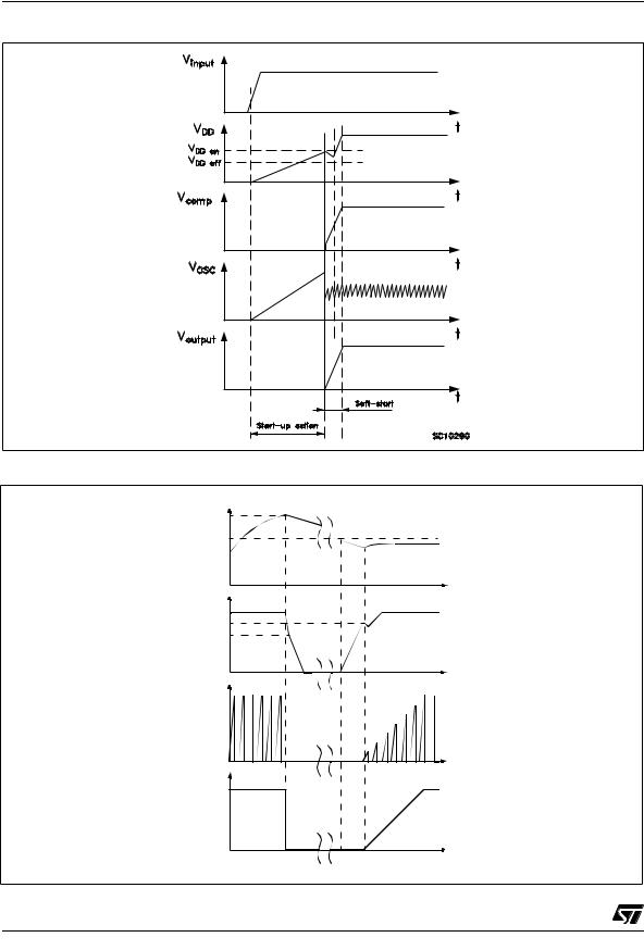
Figure 7: Start-Up Waveforms
Figure 8: Overtemperature Protection
TJ |
Ttsc |
Ttsd-Thyst |
t |
Vdd |
Vddon |
Vddoff |
t |
Id |
t
Vcomp
t |
SC10191 |
7/25
VIPer20/SP/DIP - VIPer20A/ASP/ADIP
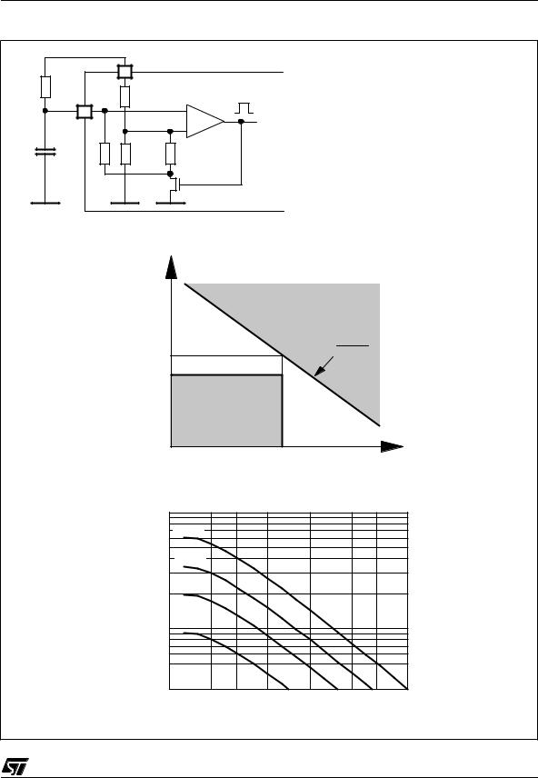
Figure 9: Oscillator
Rt |
VDD |
For Rt >1.2KW |
|
|
|
|
|
|
|||
and |
|
|
|
|
|
|
|
|
|
||
OSC |
|
|
|
|
|
|
|
|
|
||
|
Ct ³ 15nF if FSW £ 40KHz |
|
|||||||||
|
|
|
|||||||||
|
|
|
2.3 |
|
æ |
|
|
|
550 |
ö |
|
|
CLK |
FSW = |
----------- |
× è |
1 – |
--------------------- |
|||||
|
R |
C |
t |
R |
t |
– 150ø |
|||||
Ct |
Ω |
|
t |
|
|
|
|
|
|
||
~360 |
|
|
|
|
|
|
|
|
|
|
|
|
|
|
|
|
|
|
|
|
|
|
|
|
FC00050 |
|
|
|
|
|
|
|
|
|
|
|
Ct |
|
|
|
|
|
|
|
|
|
|
|
Forbidden area |
|
|
|
|
|
|
|
|
|
|
880
Ct(nF) =
Fsw(kHz)
22nF
15nF
Forbidden area
40kHz |
Fsw |
|
Oscillator frequency vs Rt and Ct
|
1,000 |
|
|
|
|
|
FC00030 |
|
|
|
|
|
|
|
|
|
|
|
|
Ct = 1.5 nF |
|
|
|
|
|
|
|
500 |
|
|
|
|
|
|
|
|
|
Ct = 2.7 nF |
|
|
|
|
|
|
(kHz) |
300 |
|
|
|
|
|
|
|
200 |
Ct = 4.7 nF |
|
|
|
|
|
|
|
|
|
|
|
|
|
|
||
Frequency |
100 |
Ct = 10 nF |
|
|
|
|
|
|
|
|
|
|
|
|
|
||
|
|
|
|
|
|
|
|
|
|
50 |
|
|
|
|
|
|
|
|
30 |
2 |
3 |
5 |
10 |
20 |
30 |
50 |
|
1 |
Rt (kΩ)
8/25
 Loading...