


ST uPSD3312D-40T6, uPSD3312DV-40T6, uPSD3333D-40T6, uPSD3333DV-40T6, uPSD3333D-40U6 User Manual
...UPSD3312D-40T6T
uPSD33xx
Turbo Series
Fast 8032 MCU with Programmable Logic
PRELIMINARY DATA
FEATURES SUMMARY
■FAST 8-BIT TURBO 8032 MCU, 40MHz
–Advanced core, 4-clocks per instruction
–10 MIPs peak performance at 40MHz (5V)
–JTAG Debug and In-System Programming
–Branch Cache & 6 instruction Prefetch Queue
–Dual XDATA pointers with auto incr & decr
–Compatible with 3rd party 8051 tools
■DUAL FLASH MEMORIES WITH MEMORY MANAGEMENT
–Place either memory into 8032 program address space or data address space
–READ-while-WRITE operation for InApplication Programming and EEPROM emulation
–Single voltage program and erase
–100K guaranteed erase cycles, 15-year retention
■CLOCK, RESET, AND SUPPLY MANAGEMENT
–SRAM is Battery Backup capable
–Flexible 8-level CPU clock divider register
–Normal, Idle, and Power Down Modes
–Power-on and Low Voltage reset supervisor
–Programmable Watchdog Timer
■PROGRAMMABLE LOGIC, GENERAL PURPOSE
–16 macrocells
–Create shifters, state machines, chipselects, glue-logic to keypads, panels, LCDs, others
■COMMUNICATION INTERFACES
–I2C Master/Slave controller, 833KHz
–SPI Master controller, 10MHz
–Two UARTs with independent baud rate
–IrDA protocol support up to 115K baud
–Up to 46 I/O, 5V tolerant on 3.3V uPSD33xxV
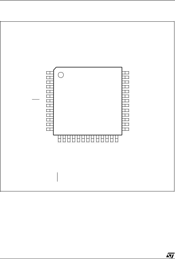
Figure 1. Packages
TQFP52 (T)
52-lead, Thin,
Quad, Flat
TQFP80 (U)
80-lead, Thin,
Quad, Flat
■A/D CONVERTER
–Eight Channels, 10-bit resolution, 6µs
■TIMERS AND INTERRUPTS
–Three 8032 standard 16-bit timers
–Programmable Counter Array (PCA), six 16-bit modules for PWM, CAPCOM, and timers
–8/10/16-bit PWM operation
–11 Interrupt sources with two external interrupt pins
■OPERATING VOLTAGE SOURCE (±10%)
–5V devices use both 5.0V and 3.3V sources
–3.3V devices use only 3.3V source
January 2005 |
1/231 |
This is preliminary information on a new product now in development or undergoing evaluation. Details are subject to change without notice.

uPSD33xx
Table 1. Device Summary
|
1st |
2nd |
SRAM |
|
8032 |
VCC |
VDD |
|
|
|
Part Number |
Flash |
Flash |
GPIO |
Pkg. |
Temp. |
|||||
(bytes) |
Bus |
|||||||||
|
(bytes) |
(bytes) |
|
|
|
|
|
|||
|
|
|
|
|
|
|
|
|||
|
|
|
|
|
|
|
|
|
|
|
uPSD3312D-40T6 |
64K |
16K |
2K |
37 |
No |
3.3V |
5.0V |
TQFP52 |
–40°C to 85°C |
|
|
|
|
|
|
|
|
|
|
|
|
uPSD3312DV-40T6 |
64K |
16K |
2K |
37 |
No |
3.3V |
3.3V |
TQFP52 |
–40°C to 85°C |
|
|
|
|
|
|
|
|
|
|
|
|
uPSD3333D-40T6 |
128K |
32K |
8K |
37 |
No |
3.3V |
5.0V |
TQFP52 |
–40°C to 85°C |
|
|
|
|
|
|
|
|
|
|
|
|
uPSD3333DV-40T6 |
128K |
32K |
8K |
37 |
No |
3.3V |
3.3V |
TQFP52 |
–40°C to 85°C |
|
|
|
|
|
|
|
|
|
|
|
|
uPSD3333D-40U6 |
128K |
32K |
8K |
46 |
Yes |
3.3V |
5.0V |
TQFP80 |
–40°C to 85°C |
|
|
|
|
|
|
|
|
|
|
|
|
uPSD3333DV-40U6 |
128K |
32K |
8K |
46 |
Yes |
3.3V |
3.3V |
TQFP80 |
–40°C to 85°C |
|
|
|
|
|
|
|
|
|
|
|
|
uPSD3334D-40U6 |
256K |
32K |
8K |
46 |
Yes |
3.3V |
5.0V |
TQFP80 |
–40°C to 85°C |
|
|
|
|
|
|
|
|
|
|
|
|
uPSD3334DV-40U6 |
256K |
32K |
8K |
46 |
Yes |
3.3V |
3.3V |
TQFP80 |
–40°C to 85°C |
|
|
|
|
|
|
|
|
|
|
|
|
uPSD3354D-40T6 |
256K |
32K |
32K |
37 |
No |
3.3V |
5.0V |
TQFP52 |
–40°C to 85°C |
|
|
|
|
|
|
|
|
|
|
|
|
uPSD3354DV-40T6 |
256K |
32K |
32K |
37 |
No |
3.3V |
3.3V |
TQFP52 |
–40°C to 85°C |
|
|
|
|
|
|
|
|
|
|
|
|
uPSD3354D-40U6 |
256K |
32K |
32K |
46 |
Yes |
3.3V |
5.0V |
TQFP80 |
–40°C to 85°C |
|
|
|
|
|
|
|
|
|
|
|
|
uPSD3354DV-40U6 |
256K |
32K |
32K |
46 |
Yes |
3.3V |
3.3V |
TQFP80 |
–40°C to 85°C |
|
|
|
|
|
|
|
|
|
|
|
2/231

uPSD33xx
TABLE OF CONTENTS
FEATURES SUMMARY . . . . . . . . . . . . . . . . . . . . . . . . . . . . . . . . . . . . . . . . . . . . . . . . . . . . . . . . . . . . . 1
SUMMARY DESCRIPTION . . . . . . . . . . . . . . . . . . . . . . . . . . . . . . . . . . . . . . . . . . . . . . . . . . . . . . . . . . . 7
PIN DESCRIPTIONS . . . . . . . . . . . . . . . . . . . . . . . . . . . . . . . . . . . . . . . . . . . . . . . . . . . . . . . . . . . . . . . . 8
uPSD33xx HARDWARE DESCRIPTION . . . . . . . . . . . . . . . . . . . . . . . . . . . . . . . . . . . . . . . . . . . . . . . 13
MEMORY ORGANIZATION . . . . . . . . . . . . . . . . . . . . . . . . . . . . . . . . . . . . . . . . . . . . . . . . . . . . . . . . . 15
Internal Memory (MCU Module, Standard 8032 Memory: DATA, IDATA, SFR) . . . . . . . . . . . . 16 External Memory (PSD Module: Program memory, Data memory). . . . . . . . . . . . . . . . . . . . . . 16
8032 MCU CORE PERFORMANCE ENHANCEMENTS . . . . . . . . . . . . . . . . . . . . . . . . . . . . . . . . . . . 17
Pre-Fetch Queue (PFQ) and Branch Cache (BC) . . . . . . . . . . . . . . . . . . . . . . . . . . . . . . . . . . . . 19
PFQ Example, Multi-cycle Instructions . . . . . . . . . . . . . . . . . . . . . . . . . . . . . . . . . . . . . . . . . . . . 19
Aggregate Performance . . . . . . . . . . . . . . . . . . . . . . . . . . . . . . . . . . . . . . . . . . . . . . . . . . . . . . . . 19
MCU MODULE DISCRIPTION . . . . . . . . . . . . . . . . . . . . . . . . . . . . . . . . . . . . . . . . . . . . . . . . . . . . . . . 21
8032 MCU REGISTERS . . . . . . . . . . . . . . . . . . . . . . . . . . . . . . . . . . . . . . . . . . . . . . . . . . . . . . . . . . . . 21
Stack Pointer (SP) . . . . . . . . . . . . . . . . . . . . . . . . . . . . . . . . . . . . . . . . . . . . . . . . . . . . . . . . . . . . . 21
Data Pointer (DPTR) . . . . . . . . . . . . . . . . . . . . . . . . . . . . . . . . . . . . . . . . . . . . . . . . . . . . . . . . . . . 21
Program Counter (PC). . . . . . . . . . . . . . . . . . . . . . . . . . . . . . . . . . . . . . . . . . . . . . . . . . . . . . . . . . 21
Accumulator (ACC) . . . . . . . . . . . . . . . . . . . . . . . . . . . . . . . . . . . . . . . . . . . . . . . . . . . . . . . . . . . . 21
B Register (B). . . . . . . . . . . . . . . . . . . . . . . . . . . . . . . . . . . . . . . . . . . . . . . . . . . . . . . . . . . . . . . . . 21
General Purpose Registers (R0 - R7). . . . . . . . . . . . . . . . . . . . . . . . . . . . . . . . . . . . . . . . . . . . . . 22
Program Status Word (PSW) . . . . . . . . . . . . . . . . . . . . . . . . . . . . . . . . . . . . . . . . . . . . . . . . . . . . 22
SPECIAL FUNCTION REGISTERS (SFR) . . . . . . . . . . . . . . . . . . . . . . . . . . . . . . . . . . . . . . . . . . . . . . 23
8032 ADDRESSING MODES . . . . . . . . . . . . . . . . . . . . . . . . . . . . . . . . . . . . . . . . . . . . . . . . . . . . . . . . 30
Register Addressing . . . . . . . . . . . . . . . . . . . . . . . . . . . . . . . . . . . . . . . . . . . . . . . . . . . . . . . . . . . 30
Direct Addressing . . . . . . . . . . . . . . . . . . . . . . . . . . . . . . . . . . . . . . . . . . . . . . . . . . . . . . . . . . . . . 30
Register Indirect Addressing . . . . . . . . . . . . . . . . . . . . . . . . . . . . . . . . . . . . . . . . . . . . . . . . . . . . 30
Immediate Addressing . . . . . . . . . . . . . . . . . . . . . . . . . . . . . . . . . . . . . . . . . . . . . . . . . . . . . . . . . 30
External Direct Addressing . . . . . . . . . . . . . . . . . . . . . . . . . . . . . . . . . . . . . . . . . . . . . . . . . . . . . 30
External Indirect Addressing . . . . . . . . . . . . . . . . . . . . . . . . . . . . . . . . . . . . . . . . . . . . . . . . . . . . 30
Indexed Addressing . . . . . . . . . . . . . . . . . . . . . . . . . . . . . . . . . . . . . . . . . . . . . . . . . . . . . . . . . . . 31
Relative Addressing . . . . . . . . . . . . . . . . . . . . . . . . . . . . . . . . . . . . . . . . . . . . . . . . . . . . . . . . . . . 31
Absolute Addressing . . . . . . . . . . . . . . . . . . . . . . . . . . . . . . . . . . . . . . . . . . . . . . . . . . . . . . . . . . 31
Long Addressing . . . . . . . . . . . . . . . . . . . . . . . . . . . . . . . . . . . . . . . . . . . . . . . . . . . . . . . . . . . . . . 31
Bit Addressing . . . . . . . . . . . . . . . . . . . . . . . . . . . . . . . . . . . . . . . . . . . . . . . . . . . . . . . . . . . . . . . . 31
uPSD33xx INSTRUCTION SET SUMMARY . . . . . . . . . . . . . . . . . . . . . . . . . . . . . . . . . . . . . . . . . . . . 32
3/231

uPSD33xx
DUAL DATA POINTERS. . . . . . . . . . . . . . . . . . . . . . . . . . . . . . . . . . . . . . . . . . . . . . . . . . . . . . . . . . . . 37
Data Pointer Control Register, DPTC (85h) . . . . . . . . . . . . . . . . . . . . . . . . . . . . . . . . . . . . . . . . . 37 Data Pointer Mode Register, DPTM (86h) . . . . . . . . . . . . . . . . . . . . . . . . . . . . . . . . . . . . . . . . . . 38
DEBUG UNIT. . . . . . . . . . . . . . . . . . . . . . . . . . . . . . . . . . . . . . . . . . . . . . . . . . . . . . . . . . . . . . . . . . . . . 39
INTERRUPT SYSTEM. . . . . . . . . . . . . . . . . . . . . . . . . . . . . . . . . . . . . . . . . . . . . . . . . . . . . . . . . . . . . . 40
Individual Interrupt Sources . . . . . . . . . . . . . . . . . . . . . . . . . . . . . . . . . . . . . . . . . . . . . . . . . . . . . 43
MCU CLOCK GENERATION . . . . . . . . . . . . . . . . . . . . . . . . . . . . . . . . . . . . . . . . . . . . . . . . . . . . . . . . 46
MCU_CLK . . . . . . . . . . . . . . . . . . . . . . . . . . . . . . . . . . . . . . . . . . . . . . . . . . . . . . . . . . . . . . . . . . . . 46 PERIPH_CLK . . . . . . . . . . . . . . . . . . . . . . . . . . . . . . . . . . . . . . . . . . . . . . . . . . . . . . . . . . . . . . . . . 46
POWER SAVING MODES . . . . . . . . . . . . . . . . . . . . . . . . . . . . . . . . . . . . . . . . . . . . . . . . . . . . . . . . . . 48
Idle Mode . . . . . . . . . . . . . . . . . . . . . . . . . . . . . . . . . . . . . . . . . . . . . . . . . . . . . . . . . . . . . . . . . . . . 48
Power-down Mode . . . . . . . . . . . . . . . . . . . . . . . . . . . . . . . . . . . . . . . . . . . . . . . . . . . . . . . . . . . . . 48
Reduced Frequency Mode . . . . . . . . . . . . . . . . . . . . . . . . . . . . . . . . . . . . . . . . . . . . . . . . . . . . . . 48
OSCILLATOR AND EXTERNAL COMPONENTS . . . . . . . . . . . . . . . . . . . . . . . . . . . . . . . . . . . . . . . . 51
I/O PORTS of MCU MODULE. . . . . . . . . . . . . . . . . . . . . . . . . . . . . . . . . . . . . . . . . . . . . . . . . . . . . . . . 53
MCU Port Operating Modes . . . . . . . . . . . . . . . . . . . . . . . . . . . . . . . . . . . . . . . . . . . . . . . . . . . . . 53
MCU BUS INTERFACE. . . . . . . . . . . . . . . . . . . . . . . . . . . . . . . . . . . . . . . . . . . . . . . . . . . . . . . . . . . . . 62
Bus Read Cycles (PSEN or RD) . . . . . . . . . . . . . . . . . . . . . . . . . . . . . . . . . . . . . . . . . . . . . . . . . . 62 Bus Write Cycles (WR) . . . . . . . . . . . . . . . . . . . . . . . . . . . . . . . . . . . . . . . . . . . . . . . . . . . . . . . . . 62 Controlling the PFQ and BC . . . . . . . . . . . . . . . . . . . . . . . . . . . . . . . . . . . . . . . . . . . . . . . . . . . . . 62
SUPERVISORY FUNCTIONS . . . . . . . . . . . . . . . . . . . . . . . . . . . . . . . . . . . . . . . . . . . . . . . . . . . . . . . . 65
External Reset Input Pin, RESET_IN . . . . . . . . . . . . . . . . . . . . . . . . . . . . . . . . . . . . . . . . . . . . . . 65
Low VCC Voltage Detect, LVD. . . . . . . . . . . . . . . . . . . . . . . . . . . . . . . . . . . . . . . . . . . . . . . . . . . . 66
Power-up Reset . . . . . . . . . . . . . . . . . . . . . . . . . . . . . . . . . . . . . . . . . . . . . . . . . . . . . . . . . . . . . . . 66
JTAG Debug Reset . . . . . . . . . . . . . . . . . . . . . . . . . . . . . . . . . . . . . . . . . . . . . . . . . . . . . . . . . . . . 66
Watchdog Timer, WDT . . . . . . . . . . . . . . . . . . . . . . . . . . . . . . . . . . . . . . . . . . . . . . . . . . . . . . . . . 66
STANDARD 8032 TIMER/COUNTERS . . . . . . . . . . . . . . . . . . . . . . . . . . . . . . . . . . . . . . . . . . . . . . . . 69
Standard Timer SFRs . . . . . . . . . . . . . . . . . . . . . . . . . . . . . . . . . . . . . . . . . . . . . . . . . . . . . . . . . . 69
Clock Sources . . . . . . . . . . . . . . . . . . . . . . . . . . . . . . . . . . . . . . . . . . . . . . . . . . . . . . . . . . . . . . . . 69
SFR, TCON . . . . . . . . . . . . . . . . . . . . . . . . . . . . . . . . . . . . . . . . . . . . . . . . . . . . . . . . . . . . . . . . . . . 71
SFR, TMOD . . . . . . . . . . . . . . . . . . . . . . . . . . . . . . . . . . . . . . . . . . . . . . . . . . . . . . . . . . . . . . . . . . . 71
Timer 0 and Timer 1 Operating Modes . . . . . . . . . . . . . . . . . . . . . . . . . . . . . . . . . . . . . . . . . . . . 71
Timer 2 . . . . . . . . . . . . . . . . . . . . . . . . . . . . . . . . . . . . . . . . . . . . . . . . . . . . . . . . . . . . . . . . . . . . . . 74
SERIAL UART INTERFACES . . . . . . . . . . . . . . . . . . . . . . . . . . . . . . . . . . . . . . . . . . . . . . . . . . . . . . . . 81
UART Operation Modes . . . . . . . . . . . . . . . . . . . . . . . . . . . . . . . . . . . . . . . . . . . . . . . . . . . . . . . . 81
4/231

uPSD33xx
Serial Port Control Registers . . . . . . . . . . . . . . . . . . . . . . . . . . . . . . . . . . . . . . . . . . . . . . . . . . . . 82 UART Baud Rates . . . . . . . . . . . . . . . . . . . . . . . . . . . . . . . . . . . . . . . . . . . . . . . . . . . . . . . . . . . . . 84 More About UART Mode 0 . . . . . . . . . . . . . . . . . . . . . . . . . . . . . . . . . . . . . . . . . . . . . . . . . . . . . . 85 More About UART Mode 1 . . . . . . . . . . . . . . . . . . . . . . . . . . . . . . . . . . . . . . . . . . . . . . . . . . . . . . 87 More About UART Modes 2 and 3 . . . . . . . . . . . . . . . . . . . . . . . . . . . . . . . . . . . . . . . . . . . . . . . . 89
IrDA INTERFACE . . . . . . . . . . . . . . . . . . . . . . . . . . . . . . . . . . . . . . . . . . . . . . . . . . . . . . . . . . . . . . . . . 92
Pulse Width Selection . . . . . . . . . . . . . . . . . . . . . . . . . . . . . . . . . . . . . . . . . . . . . . . . . . . . . . . . . . 94
I2C INTERFACE . . . . . . . . . . . . . . . . . . . . . . . . . . . . . . . . . . . . . . . . . . . . . . . . . . . . . . . . . . . . . . . . . . 95
I2C Interface Main Features . . . . . . . . . . . . . . . . . . . . . . . . . . . . . . . . . . . . . . . . . . . . . . . . . . . . . 95
Communication Flow . . . . . . . . . . . . . . . . . . . . . . . . . . . . . . . . . . . . . . . . . . . . . . . . . . . . . . . . . . 96
Operating Modes . . . . . . . . . . . . . . . . . . . . . . . . . . . . . . . . . . . . . . . . . . . . . . . . . . . . . . . . . . . . . . 98
Bus Arbitration . . . . . . . . . . . . . . . . . . . . . . . . . . . . . . . . . . . . . . . . . . . . . . . . . . . . . . . . . . . . . . . 98
Clock Synchronization . . . . . . . . . . . . . . . . . . . . . . . . . . . . . . . . . . . . . . . . . . . . . . . . . . . . . . . . . 98
General Call Address . . . . . . . . . . . . . . . . . . . . . . . . . . . . . . . . . . . . . . . . . . . . . . . . . . . . . . . . . . 98
Serial I/O Engine (SIOE) . . . . . . . . . . . . . . . . . . . . . . . . . . . . . . . . . . . . . . . . . . . . . . . . . . . . . . . . 99
I2C Interface Control Register (S1CON) . . . . . . . . . . . . . . . . . . . . . . . . . . . . . . . . . . . . . . . . . . 100
I2C Interface Status Register (S1STA) . . . . . . . . . . . . . . . . . . . . . . . . . . . . . . . . . . . . . . . . . . . . 102
I2C Data Shift Register (S1DAT). . . . . . . . . . . . . . . . . . . . . . . . . . . . . . . . . . . . . . . . . . . . . . . . . 104
I2C Address Register (S1ADR) . . . . . . . . . . . . . . . . . . . . . . . . . . . . . . . . . . . . . . . . . . . . . . . . . . 104
I2C START Sample Setting (S1SETUP) . . . . . . . . . . . . . . . . . . . . . . . . . . . . . . . . . . . . . . . . . . . 105
I2C Operating Sequences . . . . . . . . . . . . . . . . . . . . . . . . . . . . . . . . . . . . . . . . . . . . . . . . . . . . . . 108
SPI (SYNCHRONOUS PERIPHERAL INTERFACE) . . . . . . . . . . . . . . . . . . . . . . . . . . . . . . . . . . . . . 112
SPI Bus Features and Communication Flow . . . . . . . . . . . . . . . . . . . . . . . . . . . . . . . . . . . . . . 113
Full-Duplex Operation . . . . . . . . . . . . . . . . . . . . . . . . . . . . . . . . . . . . . . . . . . . . . . . . . . . . . . . . . 113
Bus-Level Activity . . . . . . . . . . . . . . . . . . . . . . . . . . . . . . . . . . . . . . . . . . . . . . . . . . . . . . . . . . . . 113
SPI SFR Registers . . . . . . . . . . . . . . . . . . . . . . . . . . . . . . . . . . . . . . . . . . . . . . . . . . . . . . . . . . . . 115
SPI Configuration . . . . . . . . . . . . . . . . . . . . . . . . . . . . . . . . . . . . . . . . . . . . . . . . . . . . . . . . . . . . 116
Dynamic Control . . . . . . . . . . . . . . . . . . . . . . . . . . . . . . . . . . . . . . . . . . . . . . . . . . . . . . . . . . . . . 116
ANALOG-TO-DIGITAL CONVERTOR (ADC) . . . . . . . . . . . . . . . . . . . . . . . . . . . . . . . . . . . . . . . . . . 120
Port 1 ADC Channel Selects . . . . . . . . . . . . . . . . . . . . . . . . . . . . . . . . . . . . . . . . . . . . . . . . . . . . 120
PROGRAMMABLE COUNTER ARRAY (PCA) WITH PWM . . . . . . . . . . . . . . . . . . . . . . . . . . . . . . . 123
PCA Block . . . . . . . . . . . . . . . . . . . . . . . . . . . . . . . . . . . . . . . . . . . . . . . . . . . . . . . . . . . . . . . . . . 123
PCA Clock Selection . . . . . . . . . . . . . . . . . . . . . . . . . . . . . . . . . . . . . . . . . . . . . . . . . . . . . . . . . . 125
Operation of TCM Modes . . . . . . . . . . . . . . . . . . . . . . . . . . . . . . . . . . . . . . . . . . . . . . . . . . . . . . 126
Capture Mode. . . . . . . . . . . . . . . . . . . . . . . . . . . . . . . . . . . . . . . . . . . . . . . . . . . . . . . . . . . . . . . . 126
Timer Mode . . . . . . . . . . . . . . . . . . . . . . . . . . . . . . . . . . . . . . . . . . . . . . . . . . . . . . . . . . . . . . . . . 126
Toggle Mode . . . . . . . . . . . . . . . . . . . . . . . . . . . . . . . . . . . . . . . . . . . . . . . . . . . . . . . . . . . . . . . . 126
PWM Mode - (X8), Fixed Frequency . . . . . . . . . . . . . . . . . . . . . . . . . . . . . . . . . . . . . . . . . . . . . . 126
PWM Mode - (X8), Programmable Frequency . . . . . . . . . . . . . . . . . . . . . . . . . . . . . . . . . . . . . . 128
PWM Mode - Fixed Frequency, 16-bit . . . . . . . . . . . . . . . . . . . . . . . . . . . . . . . . . . . . . . . . . . . . 129
5/231

uPSD33xx
PWM Mode - Fixed Frequency, 10-bit . . . . . . . . . . . . . . . . . . . . . . . . . . . . . . . . . . . . . . . . . . . . 129 Writing to Capture/Compare Registers . . . . . . . . . . . . . . . . . . . . . . . . . . . . . . . . . . . . . . . . . . . 129 Control Register Bit Definition . . . . . . . . . . . . . . . . . . . . . . . . . . . . . . . . . . . . . . . . . . . . . . . . . . 129 TCM Interrupts . . . . . . . . . . . . . . . . . . . . . . . . . . . . . . . . . . . . . . . . . . . . . . . . . . . . . . . . . . . . . . . 132
PSD MODULE . . . . . . . . . . . . . . . . . . . . . . . . . . . . . . . . . . . . . . . . . . . . . . . . . . . . . . . . . . . . . . . . . . . 133
PSD Module Functional Description . . . . . . . . . . . . . . . . . . . . . . . . . . . . . . . . . . . . . . . . . . . . . 134
Memory Mapping . . . . . . . . . . . . . . . . . . . . . . . . . . . . . . . . . . . . . . . . . . . . . . . . . . . . . . . . . . . . . 138
Runtime Control Register Definitions (csiop). . . . . . . . . . . . . . . . . . . . . . . . . . . . . . . . . . . . . . 145
PSD Module Detailed Operation. . . . . . . . . . . . . . . . . . . . . . . . . . . . . . . . . . . . . . . . . . . . . . . . . 147
PSD Module Reset Conditions . . . . . . . . . . . . . . . . . . . . . . . . . . . . . . . . . . . . . . . . . . . . . . . . . . 193
AC/DC PARAMETERS . . . . . . . . . . . . . . . . . . . . . . . . . . . . . . . . . . . . . . . . . . . . . . . . . . . . . . . . . . . . 202
MAXIMUM RATING. . . . . . . . . . . . . . . . . . . . . . . . . . . . . . . . . . . . . . . . . . . . . . . . . . . . . . . . . . . . . . . 204
DC AND AC PARAMETERS. . . . . . . . . . . . . . . . . . . . . . . . . . . . . . . . . . . . . . . . . . . . . . . . . . . . . . . . 204
PACKAGE MECHANICAL INFORMATION . . . . . . . . . . . . . . . . . . . . . . . . . . . . . . . . . . . . . . . . . . . . 225
PART NUMBERING . . . . . . . . . . . . . . . . . . . . . . . . . . . . . . . . . . . . . . . . . . . . . . . . . . . . . . . . . . . . . . 229
REVISION HISTORY. . . . . . . . . . . . . . . . . . . . . . . . . . . . . . . . . . . . . . . . . . . . . . . . . . . . . . . . . . . . . . 230
6/231

uPSD33xx
SUMMARY DESCRIPTION
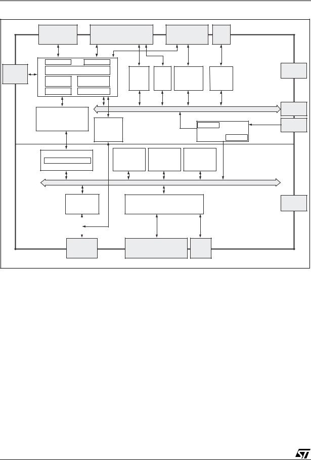
The Turbo uPSD33xx Series combines a powerful 8051-based microcontroller with a flexible memory structure, programmable logic, and a rich peripheral mix to form an ideal embedded controller. At its core is a fast 4-cycle 8032 MCU with a 6-byte instruction prefetch queue (PFQ) and a 4-entry fully associative branching cache (BC) to maximize MCU performance, enabling loops of code in smaller localities to execute extremely fast.
Code development is easily managed without a hardware In-Circuit Emulator by using the serial JTAG debug interface. JTAG is also used for InSystem Programming (ISP) in as little as 10 seconds, perfect for manufacturing and lab development. The 8032 core is coupled to Programmable System Device (PSD) architecture to optimize the 8032 memory structure, offering two independent
banks of Flash memory that can be placed at virtually any address within 8032 program or data address space, and easily paged beyond 64K bytes using on-chip programmable decode logic. Dual Flash memory banks provide a robust solution for remote product updates in the field through In-Ap- plication Programming (IAP). Dual Flash banks also support EEPROM emulation, eliminating the need for external EEPROM chips. General purpose programmable logic (PLD) is included to build an endless variety of glue-logic, saving external logic devices. The PLD is configured using the software development tool, PSDsoft Express, available from the web at www.st.com/psm, at no charge. The uPSD33xx also includes supervisor functions such as a programmable watchdog timer and low-voltage reset.
Figure 2. Block Diagram
|
|
|
|
uPSD33xx |
|
|
||
|
(3) 16-bit |
|
|
|
|
|
|
|
|
Timer/ |
Turbo |
|
PFQ |
|
1st Flash Memory: |
|
|
|
Counters |
|
|
|
||||
|
(2) |
8032 |
|
& |
|
64K, 128K, |
|
|
|
Core |
|
BC |
Programmable |
or 256K Bytes |
|
||
|
External |
|
|
|||||
|
|
|
|
|
|
|||
|
Interrupts |
|
|
|
Decode and |
|
|
|
|
|
|
|
|
Page Logic |
2nd Flash Memory: |
|
|
|
|
|
|
|
|
|
||
P3.0:7 |
|
I2C |
|
|
|
16K or 32K Bytes |
|
|
|
|
|
|
|
|
SRAM: |
|
|
|
|
|
|
|
|
2K, 8K, or 32K Bytes |
|
|
|
|
UART0 |
|
|
|
|
|
|
|
|
|
|
|
|
(8) GPIO, Port A |
PA0:7 |
|
|
|
|
|
|
|
(80-pin only) |
||
|
(8) GPIO, Port 3 |
|
|
|
||||
|
|
General |
|
|
||||
|
|
|
|
|
(8) GPIO, Port B |
PB0:7 |
||
|
|
|
|
|
Purpose |
|||
P1.0:7 |
(8) GPIO, Port 1 |
BUS |
Programmable |
|
|
|||
Logic, |
(2) GPIO, Port D |
PD1:2 |
||||||
|
|
|
|
|||||
|
|
|
|
16 Macrocells |
||||
|
|
|
|
|
|
|||
|
(8) 10-bit ADC |
|
SYSTEM |
|
(4) GPIO, Port C |
|
||
|
|
|
|
|
|
PC0:7 |
||
|
Optional IrDA |
|
|
|
|
|||
|
UART1 |
JTAG ICE and ISP |
|
|||||
|
Encoder/Decoder |
|
||||||
|
|
|
|
|
|
|||
|
|
SPI |
|
|
8032 Address/Data/Control Bus |
MCU |
||
|
|
|
|
(80-pin device only) |
Bus |
|||
|
|
|
|
|
||||
|
16-bit PCA |
|
|
Supervisor: |
|
|||
|
(6) PWM, CAPCOM, TIMER |
Watchdog and Low-Voltage Reset |
|
|||||
P4.0:7 |
(8) GPIO, Port 4 |
|
VCC, VDD, GND, Reset, Crystal In |
Dedicated |
||||
|
Pins |
|||||||
|
|
|
|
|
|
|
||
|
|
|
|
|
|
|
AI08875 |
|
|
|
|
|
|
|
|
7/231 |
|
uPSD33xx
PIN DESCRIPTIONS
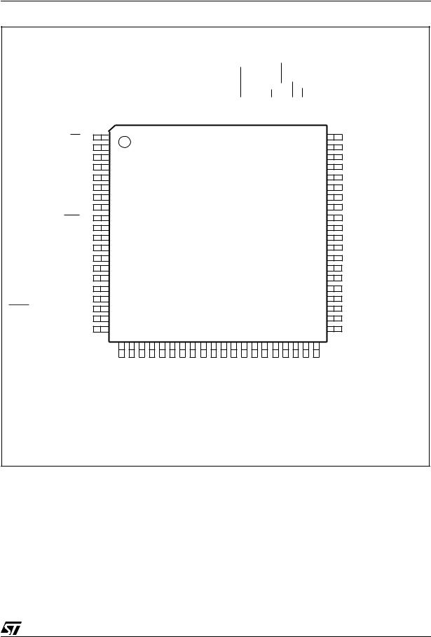
Figure 3. TQFP52 Connections
PD1/CLKIN 1 PC7 2 JTAG TDO 3 JTAG TDI 4 DEBUG 5 3.3V VCC 6
PC4/TERR 7 VDD(1) 8 GND 9
PC3/TSTAT 10 PC2/VSTBY 11 JTAG TCK 12 JTAG TMS 13
|
|
|
|
|
|
|
|
|
|
|
|
|
|
|
|
|
|
|
|
|
|
|
/ADC7 |
|
/ADC6 |
|
|
|
|
|
|
|
|
|
|
(3) REF |
|
|
|
|
|
|
|
|
|
|
|
(2) |
(2) |
||
PB0 |
PB1 |
PB2 |
|
PB3 |
PB4 |
|
PB5 |
|
|
|
RESETIN |
|
PB6 |
|
PB7 |
P1.7/SPISEL |
|
P1.6/SPITXD |
|||||||
|
|
AV |
GND |
|
|
|
|
||||||||||||||||||
|
|
|
|
|
|
|
|
|
|
/V |
|
|
|
|
|
|
|
|
|
|
|
|
|
|
|
|
|
|
|
|
|
|
|
|
|
CC |
|
|
|
|
|
|
|
|
|
|
|
|
|
|
|
52 |
|
51 |
|
50 |
49 |
|
48 |
47 |
|
46 |
|
45 |
|
44 |
43 |
42 |
|
41 |
40 |
||||||
|
|
|
|
|
|
|
|||||||||||||||||||
|
|
|
|
|
|
|
|
|
|
|
|
|
|
|
|
|
|
|
|
|
|
|
|
|
|
|
|
|
|
|
|
|
|
|
|
|
|
|
|
|
|
|
|
|
|
|
|
|
|
|
|
|
|
|
|
|
|
|
|
|
|
|
|
|
|
|
|
|
|
|
|
|
|
|
|
|
|
14 |
15 |
16 |
17 |
18 |
19 |
20 |
21 |
22 |
23 |
24 |
25 |
26 |
SPISEL |
SPITXD |
SPIRXD |
SPICLK |
TXD1(IrDA) |
GND |
RXD1(IrDA) |
T2X |
T2 |
RXD0/P3.0 |
TXD0/P3.1 |
EXTINT0/TG0/P3.2 |
EXTINT1/TG1/P3.3 |
/PCACLK1/P4.7 |
(2) |
(2) |
(2) |
/PCACLK0/P4.3 |
|
(2) |
(2) |
(2) |
|
|
|
|
|
/TCM5/P4.6 |
/TCM4/P4.5 |
/TCM3/P4.4 |
|
|
/TCM2/P4.2 |
/TCM1/P4.1 |
/TCM0/P4.0 |
|
|
|
|
(2) |
|
|
|
(2) |
|
|
|
|
|
|
|
|
39 P1.5/SPIRXD(2)/ADC5
38 P1.4/SPICLK(2)/ADC4
37 P1.3/TXD1(IrDA)(2)/ADC3
36 P1.2/RXD1(IrDA)(2)/ADC2
35 P1.1/T2X(2)/ADC1
34 P1.0/T2(2)/ADC0
33 VDD(1)
32 XTAL2
31 XTAL1
30 P3.7/SCL
29 P3.6/SDA
28 P3.5/C1
27 P3.4/C0
AI07822
Note: 1. For 5V applications, VDD must be connected to a 5.0V source. For 3.3V applications, VDD must be connected to a 3.3V source.
2.These signals can be used on one of two different ports (Port 1 or Port 4) for flexibility. Default is Port1.
3.VREF and 3.3V AVCC are shared in the 52-pin package only. ADC channels must use AVCC as VREF for the 52-pin package.
8/231
uPSD33xx
Figure 4. TQFP80 Connections
PD2/CSI 1
P3.3/TG1/EXINT1 2
PD1/CLKIN 3
ALE 4
PC7 5
JTAG TDO 6
JTAG TDI 7
DEBUG 8
PC4/TERR 9
3.3V VCC 10
NC 11
VDD(1) 12
GND 13
PC3/TSTAT 14
PC2/VSTBY 15
JTAG TCK 16
NC 17
SPISEL(2)/PCACLK1/P4.7 18
SPITXD(2)/TCM5/P4.6 19
JTAG TMS 20
PB0 |
P3.2/EXINT0/TG0 |
PB1 |
P3.1/TXD0 |
PB2 |
P3.0/RXD0 |
PB3 |
PB4 |
AV |
PB5 |
V |
GND |
RESETIN |
PB6 |
PB7 |
RD |
|
/ADC7 |
|
PSEN |
WR |
|
/ADC6 |
||||||||||||||||
|
P1.7/SPISEL |
|
|
P1.6/SPITXD |
||||||||||||||||||||||||||||||||||
|
|
|
|
|
|
|
|
|
|
|
|
|
|
|
|
|
|
|
|
|
|
|
|
|
|
|
|
|
|
|
(2) |
|
|
|
|
(2) |
||
|
|
|
|
|
|
|
|
|
|
|
|
|
|
|
|
CC |
|
|
REF |
|
|
|
|
|
|
|
|
|
|
|
|
|
|
|
|
|
||
80 |
79 |
78 |
77 |
76 |
75 |
74 |
73 |
72 |
|
71 |
70 |
69 |
68 |
67 |
|
66 |
|
65 |
64 |
63 |
|
62 |
61 |
|||||||||||||||
|
|
|
|
|
|
|
|
|
|
|
|
|
|
|
|
|
|
|
|
|
|
|
|
|
|
|
|
|
|
|
|
|
|
|
|
|
|
|
|
|
|
|
|
|
|
|
|
|
|
|
|
|
|
|
|
|
|
|
|
|
|
|
|
|
|
|
|
|
|
|
|
|
|
|
|
|
|
|
|
|
|
|
|
|
|
|
|
|
|
|
|
|
|
|
|
|
|
|
|
|
|
|
|
|
|
|
|
|
|
|
|
|
|
|
|
|
21 |
22 |
23 |
24 |
25 |
26 |
27 |
28 |
29 |
30 |
31 |
32 |
33 |
34 |
35 |
36 |
37 |
38 |
39 |
40 |
PA7 |
PA6 |
(2) |
PA5 |
(2) |
PA4 |
/PCACLK0/P4.3 |
PA3 |
GND |
(2) |
(2) |
PA2 |
(2) |
PA1 |
PA0 |
MCUAD0 |
MCUAD1 |
MCUAD2 |
MCUAD3 |
P3.4/C0 |
|
|
/TCM4/P4.5 |
|
/TCM3/P4.4 |
|
TXD1(IrDA) |
|
|
/TCM2/P4.2 |
/TCM1/P4.1 |
|
/TCM0/P4.0 |
|
|
|
|
|
|
|
|
|
SPIRXD |
|
SPICLK |
|
|
|
RXD1(IrDA) |
T2X |
|
T2 |
|
|
|
|
|
|
|
|
|
|
|
|
|
|
(2) |
|
|
|
|
|
|
|
|
|
|
|
|
|
60 |
P1.5/SPIRXD(2)/ADC5 |
59 |
P1.4/SPICLK(2)/ADC4 |
58 |
P1.3/TXD1(IrDA)(2)/ADC3 |
57 |
MCU A11 |
56 |
P1.2/RXD1(IrDA)(2)/ADC2 |
55 |
MCU A10 |
54 |
P1.1/T2X(2)/ADC1 |
53 |
MCU A9 |
52 |
P1.0/T2(2)/ADC0 |
51 |
MCU A8 |
50 |
(1) |
VDD |
|
49 |
XTAL2 |
48 |
XTAL1 |
47 |
MCU AD7 |
46 |
P3.7/SCL |
45 |
MCU AD6 |
44 |
P3.6/SDA |
43 |
MCU AD5 |
42 |
P3.5/C1 |
41 |
MCU AD4 |
AI07823
Note: NC = Not Connected
Note: 1. For 5V applications, VDD must be connected to a 5.0V source. For 3.3V applications, VDD must be connected to a 3.3V source. 2. These signals can be used on one of two different ports (Port 1 or Port 4) for flexibility. Default is Port1.
9/231

uPSD33xx
Table 2. Pin Definitions
Port Pin |
|
Signal |
80-Pin |
52-Pin |
In/Out |
|
Function |
|
|
|
Name |
No. |
No.(1) |
Basic |
Alternate 1 |
Alternate 2 |
|||
|
|
|
|||||||
|
|
|
|
|
|
|
External Bus |
|
|
MCUAD0 |
|
AD0 |
36 |
N/A |
I/O |
Multiplexed Address/ |
|
|
|
|
|
|
|
|
|
|
Data bus A0/D0 |
|
|
|
|
|
|
|
|
|
|
|
|
MCUAD1 |
|
AD1 |
37 |
N/A |
I/O |
Multiplexed Address/ |
|
|
|
|
Data bus A1/D1 |
|
|
||||||
|
|
|
|
|
|
|
|
|
|
|
|
|
|
|
|
|
|
|
|
MCUAD2 |
|
AD2 |
38 |
N/A |
I/O |
Multiplexed Address/ |
|
|
|
|
Data bus A2/D2 |
|
|
||||||
|
|
|
|
|
|
|
|
|
|
|
|
|
|
|
|
|
|
|
|
MCUAD3 |
|
AD3 |
39 |
N/A |
I/O |
Multiplexed Address/ |
|
|
|
|
Data bus A3/D3 |
|
|
||||||
|
|
|
|
|
|
|
|
|
|
|
|
|
|
|
|
|
|
|
|
MCUAD4 |
|
AD4 |
41 |
N/A |
I/O |
Multiplexed Address/ |
|
|
|
|
Data bus A4/D4 |
|
|
||||||
|
|
|
|
|
|
|
|
|
|
|
|
|
|
|
|
|
|
|
|
MCUAD5 |
|
AD5 |
43 |
N/A |
I/O |
Multiplexed Address/ |
|
|
|
|
Data bus A5/D5 |
|
|
||||||
|
|
|
|
|
|
|
|
|
|
|
|
|
|
|
|
|
|
|
|
MCUAD6 |
|
AD6 |
45 |
N/A |
I/O |
Multiplexed Address/ |
|
|
|
|
Data bus A6/D6 |
|
|
||||||
|
|
|
|
|
|
|
|
|
|
|
|
|
|
|
|
|
|
|
|
MCUAD7 |
|
AD7 |
47 |
N/A |
I/O |
Multiplexed Address/ |
|
|
|
|
Data bus A7/D7 |
|
|
||||||
|
|
|
|
|
|
|
|
|
|
|
|
|
|
|
|
|
|
|
|
MCUA8 |
|
A8 |
51 |
N/A |
O |
External Bus, Addr |
|
|
|
|
A8 |
|
|
||||||
|
|
|
|
|
|
|
|
|
|
|
|
|
|
|
|
|
|
|
|
MCUA9 |
|
A9 |
53 |
N/A |
O |
External Bus, Addr |
|
|
|
|
A9 |
|
|
||||||
|
|
|
|
|
|
|
|
|
|
|
|
|
|
|
|
|
|
|
|
MCUA10 |
|
A10 |
55 |
N/A |
O |
External Bus, Addr |
|
|
|
|
A10 |
|
|
||||||
|
|
|
|
|
|
|
|
|
|
|
|
|
|
|
|
|
|
|
|
MCUA11 |
|
A11 |
57 |
N/A |
O |
External Bus, Addr |
|
|
|
|
A11 |
|
|
||||||
|
|
|
|
|
|
|
|
|
|
|
|
|
|
|
|
|
|
|
|
P1.0 |
|
T2 |
52 |
34 |
I/O |
General I/O port pin |
Timer 2 Count input |
ADC Channel 0 |
|
|
ADC0 |
(T2) |
input (ADC0) |
||||||
|
|
|
|
|
|
||||
|
|
|
|
|
|
|
|
|
|
P1.1 |
|
T2X |
54 |
35 |
I/O |
General I/O port pin |
Timer 2 Trigger input |
ADC Channel 1 |
|
|
ADC1 |
(T2X) |
input (ADC1) |
||||||
|
|
|
|
|
|
||||
|
|
|
|
|
|
|
|
|
|
P1.2 |
|
RxD1 |
56 |
36 |
I/O |
General I/O port pin |
UART1 or IrDA |
ADC Channel 2 |
|
|
ADC2 |
Receive (RxD1) |
input (ADC2) |
||||||
|
|
|
|
|
|
||||
|
|
|
|
|
|
|
|
|
|
P1.3 |
|
TXD1 |
58 |
37 |
I/O |
General I/O port pin |
UART or IrDA |
ADC Channel 3 |
|
|
ADC3 |
Transmit (TxD1) |
input (ADC3) |
||||||
|
|
|
|
|
|
||||
|
|
|
|
|
|
|
|
||
P1.4 |
SPICLK |
59 |
38 |
I/O |
General I/O port pin |
SPI Clock Out |
ADC Channel 4 |
||
|
ADC4 |
(SPICLK) |
input (ADC4) |
||||||
|
|
|
|
|
|
||||
|
|
|
|
|
|
|
|
||
P1.5 |
SPIRxD |
60 |
39 |
I/O |
General I/O port pin |
SPI Receive |
ADC Channel 5 |
||
|
ADC6 |
(SPIRxD) |
input (ADC5) |
||||||
|
|
|
|
|
|
||||
|
|
|
|
|
|
|
|
||
P1.6 |
SPITXD |
61 |
40 |
I/O |
General I/O port pin |
SPI Transmit |
ADC Channel 6 |
||
|
ADC6 |
(SPITxD) |
input (ADC6) |
||||||
|
|
|
|
|
|
||||
|
|
|
|
|
|
|
|
|
|
P1.7 |
|
SPISEL |
|
64 |
41 |
I/O |
General I/O port pin |
SPI Slave Select |
ADC Channel 7 |
|
ADC7 |
(SPISEL) |
input (ADC7) |
||||||
|
|
|
|
|
|
||||
|
|
|
|
|
|
|
|
|
|
P3.0 |
|
RxD0 |
75 |
23 |
I/O |
General I/O port pin |
UART0 Receive |
|
|
|
(RxD0) |
|
|||||||
|
|
|
|
|
|
|
|
|
|
|
|
|
|
|
|
|
|
|
|
P3.1 |
|
TXD0 |
77 |
24 |
I/O |
General I/O port pin |
UART0 Transmit |
|
|
|
(TxD0) |
|
|||||||
|
|
|
|
|
|
|
|
|
|
|
|
|
|
|
|
|
|
|
|
|
EXINT0 |
|
|
|
|
Interrupt 0 input |
|
||
P3.2 |
79 |
25 |
I/O |
General I/O port pin |
(EXTINT0)/Timer 0 |
|
|||
|
TGO |
|
|||||||
|
|
|
|
|
|
gate control (TG0) |
|
||
|
|
|
|
|
|
|
|
|
|
|
|
|
|
|
|
|
|
|
|
|
|
|
|
|
|
|
|
Interrupt 1 input |
|
P3.3 |
|
INT1 |
2 |
26 |
I/O |
General I/O port pin |
(EXTINT1)/Timer 1 |
|
|
|
|
|
|
|
|
|
|
gate control (TG1) |
|
|
|
|
|
|
|
|
|
|
|
P3.4 |
|
C0 |
40 |
27 |
I/O |
General I/O port pin |
Counter 0 input (C0) |
|
|
|
|
|
|
|
|
|
|
|
|
10/231
|
|
|
|
|
|
|
|
|
|
|
|
|
|
|
|
uPSD33xx |
|
|
|
|
|
|
|
|
|
|
|
|
|
|
|
|
|
|
Port Pin |
|
|
Signal |
80-Pin |
52-Pin |
In/Out |
|
Function |
|
|
|||||
|
|
|
Name |
No. |
No.(1) |
Basic |
Alternate 1 |
|
Alternate 2 |
|||||||
|
|
|
|
|
|
|
|
|
|
|||||||
|
|
P3.5 |
|
|
C1 |
42 |
28 |
I/O |
General I/O port pin |
Counter 1 input (C1) |
|
|
||||
|
|
|
|
|
|
|
|
|
|
|
|
|
|
|
|
|
|
|
P3.6 |
|
|
SDA |
44 |
29 |
I/O |
General I/O port pin |
I2C Bus serial data |
|
|
||||
|
|
|
|
(I2CSDA) |
|
|
||||||||||
|
|
|
|
|
|
|
|
|
|
|
|
|
|
|
|
|
|
|
P3.7 |
|
|
SCL |
46 |
30 |
I/O |
General I/O port pin |
I2C Bus clock |
|
|
||||
|
|
|
|
(I2CSCL) |
|
|
||||||||||
|
|
|
|
|
|
|
|
|
|
|
|
|
|
|
|
|
|
|
P4.0 |
|
|
T2 |
33 |
22 |
I/O |
General I/O port pin |
Program Counter |
Timer 2 Count input |
|||||
|
|
|
|
TCM0 |
Array0 PCA0-TCM0 |
(T2) |
|
|||||||||
|
|
|
|
|
|
|
|
|
|
|
|
|
||||
|
|
|
|
|
|
|
|
|
|
|
|
|
|
|
||
|
|
P4.1 |
|
|
T2X |
31 |
21 |
I/O |
General I/O port pin |
PCA0-TCM1 |
Timer 2 Trigger input |
|||||
|
|
|
|
TCM1 |
(T2X) |
|||||||||||
|
|
|
|
|
|
|
|
|
|
|
|
|
||||
|
|
|
|
|
|
|
|
|
|
|
|
|
|
|
||
|
|
P4.2 |
|
|
RXD1 |
30 |
20 |
I/O |
General I/O port pin |
PCA0-TCM2 |
UART1 or IrDA |
|||||
|
|
|
|
TCM2 |
Receive (RxD1) |
|||||||||||
|
|
|
|
|
|
|
|
|
|
|
|
|
||||
|
|
|
|
|
|
|
|
|
|
|
|
|
|
|
||
|
|
P4.3 |
|
|
TXD1 |
27 |
18 |
I/O |
General I/O port pin |
PCACLK0 |
UART1 or IrDA |
|||||
|
|
|
PCACLK0 |
Transmit (TxD1) |
||||||||||||
|
|
|
|
|
|
|
|
|
|
|
|
|||||
|
|
|
|
|
|
|
|
|
|
|
|
|
|
|||
|
|
P4.4 |
|
SPICLK |
25 |
17 |
I/O |
General I/O port pin |
Program Counter |
SPI Clock Out |
||||||
|
|
|
|
TCM3 |
Array1 PCA1-TCM3 |
(SPICLK) |
||||||||||
|
|
|
|
|
|
|
|
|
|
|
|
|||||
|
|
|
|
|
|
|
|
|
|
|
|
|
|
|||
|
|
P4.5 |
|
SPIRXD |
23 |
16 |
I/O |
General I/O port pin |
PCA1-TCM4 |
SPI Receive |
||||||
|
|
|
|
TCM4 |
(SPIRxD) |
|||||||||||
|
|
|
|
|
|
|
|
|
|
|
|
|
||||
|
|
|
|
|
|
|
|
|
|
|
|
|
|
|
|
|
|
|
P4.6 |
|
SPITXD |
19 |
15 |
I/O |
General I/O port pin |
PCA1-TCM5 |
SPI Transmit |
||||||
|
|
|
(SPITxD) |
|||||||||||||
|
|
|
|
|
|
|
|
|
|
|
|
|
|
|
||
|
|
|
|
|
|
|
|
|
|
|
|
|
|
|
|
|
|
|
P4.7 |
|
|
SPISEL |
|
18 |
14 |
I/O |
General I/O port pin |
PCACLK1 |
SPI Slave Select |
||||
|
|
|
PCACLK1 |
(SPISEL) |
||||||||||||
|
|
|
|
|
|
|
|
|
|
|
|
|||||
|
|
|
|
|
|
|
|
|
|
|
|
|
|
|
|
|
|
|
VREF |
|
|
|
|
70 |
N/A |
I |
Reference Voltage |
|
|
|
|||
|
|
|
|
|
|
input for ADC |
|
|
|
|||||||
|
|
|
|
|
|
|
|
|
|
|
|
|
|
|
|
|
|
|
|
|
|
|
|
|
|
|
|
|
|
|
|
|
|
|
|
|
|
|
|
|
|
|
|
65 |
N/A |
O |
READ Signal, |
|
|
|
|
|
|
RD |
|
|
|
|
|
|
|
||||||
|
|
|
|
|
|
|
external bus |
|
|
|
||||||
|
|
|
|
|
|
|
|
|
|
|
|
|
|
|
|
|
|
|
|
|
|
|
|
|
|
|
|
|
|
|
|
|
|
|
|
|
|
|
|
|
|
|
|
62 |
N/A |
O |
WRITE Signal, |
|
|
|
|
|
WR |
|
|
|
|
|
|
|
|||||||
|
|
|
|
|
|
external bus |
|
|
|
|||||||
|
|
|
|
|
|
|
|
|
|
|
|
|
|
|
|
|
|
|
|
|
|
|
|
|
|
|
|
|
|
|
|
|
|
|
|
|
|
|
|
|
|
|
|
63 |
N/A |
O |
PSEN Signal, |
|
|
|
|
PSEN |
|
|
|
|
|
|
|
||||||||
|
|
|
|
|
external bus |
|
|
|
||||||||
|
|
|
|
|
|
|
|
|
|
|
|
|
|
|
|
|
|
|
|
|
|
|
|
|
|
|
|
|
|
|
|
|
|
|
|
ALE |
|
|
|
|
4 |
N/A |
O |
Address Latch |
|
|
|
|||
|
|
|
|
|
|
signal, external bus |
|
|
|
|||||||
|
|
|
|
|
|
|
|
|
|
|
|
|
|
|
|
|
|
|
|
|
|
|
|
|
|
|
|
|
|
|
|
|
|
|
|
|
|
|
|
|
|
|
|
68 |
44 |
I |
Active low reset |
|
|
|
RESET_IN |
|
|
|
|
|
|
|
|||||||||
|
|
|
|
input |
|
|
|
|||||||||
|
|
|
|
|
|
|
|
|
|
|
|
|
|
|
|
|
|
|
|
|
|
|
|
|
|
|
|
|
|
|
|
|
|
|
XTAL1 |
|
|
|
|
48 |
31 |
I |
Oscillator input pin |
|
|
|
||||
|
|
|
|
|
for system clock |
|
|
|
||||||||
|
|
|
|
|
|
|
|
|
|
|
|
|
|
|
|
|
|
|
|
|
|
|
|
|
|
|
|
|
|
|
|
|
|
|
XTAL2 |
|
|
|
|
49 |
32 |
O |
Oscillator output pin |
|
|
|
||||
|
|
|
|
|
for system clock |
|
|
|
||||||||
|
|
|
|
|
|
|
|
|
|
|
|
|
|
|
|
|
|
|
|
|
|
|
|
|
|
|
|
|
|
|
|
|
|
|
DEBUG |
|
|
|
|
8 |
5 |
I/O |
I/O to the MCU |
|
|
|
||||
|
|
|
|
|
Debug Unit |
|
|
|
||||||||
|
|
|
|
|
|
|
|
|
|
|
|
|
|
|
|
|
|
|
|
|
|
|
|
|
|
|
|
|
|
||||
|
|
PA0 |
|
|
|
|
35 |
N/A |
I/O |
General I/O port pin |
|
All Port A pins |
||||
|
|
PA1 |
|
|
|
|
34 |
N/A |
I/O |
General I/O port pin |
|
support: |
||||
|
|
|
|
|
|
|
|
|
|
|
|
|
|
|
1. |
PLD Macro-cell |
|
|
PA2 |
|
|
|
|
32 |
N/A |
I/O |
General I/O port pin |
|
|||||
|
|
|
|
|
|
|
|
outputs, or |
||||||||
|
|
|
|
|
|
|
|
|
|
|
|
|
|
|
|
|
|
|
PA3 |
|
|
|
|
28 |
N/A |
I/O |
General I/O port pin |
|
|
||||
|
|
|
|
|
|
|
2. |
PLD inputs, or |
||||||||
|
|
|
|
|
|
|
|
|
|
|
|
|
|
|
||
|
|
PA4 |
|
|
|
|
26 |
N/A |
I/O |
General I/O port pin |
|
3. |
Latched |
|||
|
|
|
|
|
|
|
|
|
|
|
|
|
|
|
|
Address Out |
|
|
PA5 |
|
|
|
|
24 |
N/A |
I/O |
General I/O port pin |
|
|
||||
|
|
|
|
|
|
|
|
(A0-A7), or |
||||||||
|
|
|
|
|
|
|
|
|
|
|
|
|
|
|
|
|
|
|
PA6 |
|
|
|
|
22 |
N/A |
I/O |
General I/O port pin |
|
|
||||
|
|
|
|
|
|
|
4. |
Peripheral I/O |
||||||||
|
|
PA7 |
|
|
|
|
21 |
N/A |
I/O |
General I/O port pin |
|
|
Mode |
|||
|
|
|
|
|
|
|
|
|
|
|
|
|
|
|
|
|
11/231

uPSD33xx
Port Pin |
Signal |
80-Pin |
52-Pin |
In/Out |
|
Function |
|
|
|||
Name |
No. |
No.(1) |
Basic |
Alternate 1 |
|
Alternate 2 |
|||||
|
|
|
|||||||||
PB0 |
|
|
|
80 |
52 |
I/O |
General I/O port pin |
|
|
|
|
|
|
|
|
|
|
|
|
|
All Port B pins |
||
PB1 |
|
|
|
78 |
51 |
I/O |
General I/O port pin |
|
|||
|
|
|
|
|
|
|
|
|
support: |
||
PB2 |
|
|
|
76 |
50 |
I/O |
General I/O port pin |
|
|||
|
|
|
|
1. |
PLD Macro-cell |
||||||
|
|
|
|
|
|
|
|
|
|||
PB3 |
|
|
|
74 |
49 |
I/O |
General I/O port pin |
|
|||
|
|
|
|
|
outputs, or |
||||||
|
|
|
|
|
|
|
|
|
|
||
PB4 |
|
|
|
73 |
48 |
I/O |
General I/O port pin |
|
2. |
PLD inputs, or |
|
|
|
|
|
|
|
|
|
|
3. |
Latched |
|
PB5 |
|
|
|
71 |
46 |
I/O |
General I/O port pin |
|
|||
|
|
|
|
|
Address Out |
||||||
|
|
|
|
|
|
|
|
|
|
||
PB6 |
|
|
|
67 |
43 |
I/O |
General I/O port pin |
|
|
||
|
|
|
|
|
(A0-A7) |
||||||
PB7 |
|
|
|
66 |
42 |
I/O |
General I/O port pin |
|
|
|
|
|
|
|
|
|
|
|
|
|
|
||
JTAGTMS |
|
TMS |
20 |
13 |
I |
JTAG pin (TMS) |
|
|
|
||
|
|
|
|
|
|
|
|
|
|
||
JTAGTCK |
|
TCK |
16 |
12 |
I |
JTAG pin (TCK) |
|
|
|
||
|
|
|
|
|
|
|
|
|
|
|
|
|
|
|
|
|
|
|
|
SRAM Standby |
|
PLD Macrocell |
|
PC2 |
VSTBY |
15 |
11 |
I/O |
General I/O port pin |
voltage input |
|
||||
output, or PLD input |
|||||||||||
|
|
|
|
|
|
|
|
(VSTBY) |
|||
|
|
|
|
|
|
|
|
|
|
||
PC3 |
TSTAT |
14 |
10 |
I/O |
General I/O port pin |
Optional JTAG |
|
PLD, Macrocell |
|||
Status (TSTAT) |
output, or PLD input |
||||||||||
|
|
|
|
|
|
|
|
||||
|
|
|
|
|
|
|
|
|
|
|
|
|
|
|
|
9 |
7 |
I/O |
General I/O port pin |
Optional JTAG |
|
PLD, Macrocell |
|
PC4 |
TERR |
|
|||||||||
Status (TERR) |
output, or PLD input |
||||||||||
|
|
|
|
|
|
|
|
||||
|
|
|
|
|
|
|
|
|
|
||
JTAGTDI |
|
TDI |
7 |
4 |
I |
JTAG pin (TDI) |
|
|
|
||
|
|
|
|
|
|
|
|
|
|
||
JTAGTDO |
|
TDO |
6 |
3 |
O |
JTAG pin (TDO) |
|
|
|
||
|
|
|
|
|
|
|
|
|
|
|
|
PC7 |
|
|
|
5 |
2 |
I/O |
General I/O port pin |
|
|
PLD, Macrocell |
|
|
|
|
|
output, or PLD input |
|||||||
|
|
|
|
|
|
|
|
|
|||
|
|
|
|
|
|
|
|
|
|
|
|
PD1 |
CLKIN |
3 |
1 |
I/O |
General I/O port pin |
|
1. |
PLD I/O |
|||
|
2. |
Clock input to |
|||||||||
|
|
|
|
|
|
|
|
|
|
PLD and APD |
|
|
|
|
|
|
|
|
|
|
|
|
|
PD2 |
|
CSI |
1 |
N/A |
I/O |
General I/O port pin |
|
1. |
PLD I/O |
||
|
|
2. |
Chip select ot |
||||||||
|
|
|
|
|
|
|
|
|
|
PSD Module |
|
|
|
|
|
|
|
|
|
|
|
|
|
3.3V-VCC |
|
|
|
10 |
6 |
|
VCC - MCU Module |
|
|
|
|
AVCC |
|
|
|
72 |
47 |
|
Analog VCC Input |
|
|
|
|
VDD |
|
|
|
|
|
|
VDD - PSD Module |
|
|
|
|
|
|
|
12 |
8 |
|
VDD - 3.3V for 3V |
|
|
|
||
3.3V or 5V |
|
|
|
|
|
|
|
||||
|
|
|
|
|
|
VDD - 5V for 5V |
|
|
|
||
|
|
|
|
|
|
|
|
|
|
||
VDD |
|
|
|
|
|
|
VDD - PSD Module |
|
|
|
|
|
|
|
50 |
33 |
|
VDD - 3.3V for 3V |
|
|
|
||
3.3V or 5V |
|
|
|
|
|
|
|
||||
|
|
|
|
|
|
VDD - 5V for 5V |
|
|
|
||
|
|
|
|
|
|
|
|
|
|
||
GND |
|
|
|
13 |
9 |
|
|
|
|
|
|
|
|
|
|
|
|
|
|
|
|
|
|
GND |
|
|
|
29 |
19 |
|
|
|
|
|
|
|
|
|
|
|
|
|
|
|
|
|
|
GND |
|
|
|
69 |
45 |
|
|
|
|
|
|
|
|
|
|
|
|
|
|
|
|
|
|
NC |
|
|
|
11 |
N/A |
|
|
|
|
|
|
|
|
|
|
|
|
|
|
|
|
|
|
NC |
|
|
|
17 |
N/A |
|
|
|
|
|
|
|
|
|
|
|
|
|
|
|
|
|
|
Note: 1. N/A = Signal Not Available on 52-pin package.
12/231

uPSD33xx
uPSD33xx HARDWARE DESCRIPTION
The uPSD33xx has a modular architecture built from a stacked die process. There are two die, one is designated “MCU Module” in this document, and the other is designated “PSD Module” (seeFigure 5., page 14). In all cases, the MCU Module die operates at 3.3V with 5V tolerant I/O. The PSD Module is either a 3.3V die or a 5V die, depending on the uPSD33xx device as described below.
The MCU Module consists of a fast 8032 core, that operates with 4 clocks per instruction cycle, and has many peripheral and system supervisor functions. The PSD Module provides the 8032 with multiple memories (two Flash and one SRAM) for program and data, programmable logic for address decoding and for general-purpose logic, and additional I/O. The MCU Module communicates with the PSD Module through internal address and data busses (A8 – A15, AD0 – AD7) and control signals (RD, WR, PSEN, ALE, RESET).
There are slightly different I/O characteristics for each module. I/Os for the MCU module are designated as Ports 1, 3, and 4. I/Os for the PSD Module are designated as Ports A, B, C, and D.
For all 5V uPSD33xx devices, a 3.3V MCU Module is stacked with a 5V PSD Module. In this case, a 5V uPSD33xx device must be supplied with 3.3VCC for the MCU Module and 5.0VDD for the PSD Module. Ports 3 and 4 of the MCU Module are 3.3V ports with tolerance to 5V devices (they can be directly driven by external 5V devices and they can directly drive external 5V devices while
producing a VOH of 2.4V min and VCC max). Ports A, B, C, and D of the PSD Module are true 5V ports.
For all 3.3V uPSD33xxV devices, a 3.3V MCU Module is stacked with a 3.3V PSD Module. In this case, a 3.3V uPSD33xx device needs to be supplied with a single 3.3V voltage source at both VCC and VDD. I/O pins on Ports 3 and 4 are 5V tolerant and can be connected to external 5V peripherals devices if desired. Ports A, B, C, and D of the PSD Module are 3.3V ports, which are not tolerant to external 5V devices.
Refer to Table 3 for port type and voltage source requirements.
80-pin uPSD33xx devices provide access to 8032 address, data, and control signals on external pins to connect external peripheral and memory devices. 52-pin uPSD33xx devices do not provide access to the 8032 system bus.
All non-volatile memory and configuration portions of the uPSD33xx device are programmed through the JTAG interface and no special programming voltage is needed. This same JTAG port is also used for debugging of the 8032 core at runtime providing breakpoint, single-step, display, and trace features. A non-volatile security bit may be programmed to block all access via JTAG interface for security. The security bit is defeated only by erasing the entire device, leaving the device blank and ready to use again.
Table 3. Port Type and Voltage Source Combinations
Device Type |
VCC for MCU |
VDD for PSD |
Ports 3 and 4 on |
Ports A, B, C, and D on |
|
Module |
Module |
MCU Module |
PSD Module |
||
|
|||||
|
|
|
|
|
|
5V: |
3.3V |
5.0V |
3.3V but 5V tolerant |
5V |
|
uPSD33xx |
|||||
|
|
|
|
||
|
|
|
|
|
|
3.3V: |
3.3V |
3.3V |
3.3V but 5V tolerant |
3.3V. NOT 5V tolerant |
|
uPSD33xxV |
|||||
|
|
|
|
||
|
|
|
|
|
13/231
uPSD33xx
Figure 5. uPSD33xx Functional Modules
|
Port 3 - UART0, |
Port 1 - Timer, ADC, SPI |
|
|
Port 4 - PCA, |
Port 3 |
|
|
||||
|
Intr, Timers |
|
|
|
PWM, UART1 |
I2C |
|
|
||||
|
|
|
|
|
|
|
|
|
|
|
MCU Module |
|
|
Port 3 |
|
Port 1 |
|
|
|
|
|
|
|
|
|
XTAL |
Turbo 8032 Core |
|
|
|
|
PCA |
|
|
|
VCC Pins |
||
10-bit |
|
|
|
2 |
|
|
3.3V |
|||||
|
|
|
|
|
|
|
|
|||||
Clock Unit |
Dual |
|
3 Timer / |
|
SPI |
|
PWM |
I C |
|
|
||
|
ADC |
|
|
|
|
|||||||
|
UARTs |
|
Counters |
|
|
|
Counters |
Unit |
|
|
||
|
|
|
|
|
|
|
|
|
|
|
|
|
|
Interrupt |
256 Byte SRAM |
|
|
|
|
|
|
|
|
|
|
|
|
|
|
8032 Internal |
Bus |
|
|
|
|
|
Ext. |
|
|
Dedicated Memory |
|
|
|
|
|
|
Bus |
||||
|
|
|
|
|
|
|
|
|
|
|||
|
Interface Prefetch, |
|
|
|
|
|
|
|
|
Reset Input |
Reset |
|
|
Branch Cache |
|
|
|
|
|
LVD |
|
||||
|
JTAG |
|
|
|
|
|
|
|||||
|
|
|
|
|
|
|
Pin |
|||||
|
|
|
|
|
|
|
Internal |
Reset Logic |
|
|||
|
|
|
DEBUG |
|
|
|
|
|
|
|||
|
|
|
|
|
|
|
Reset |
|
WDT |
|
|
|
8-Bit Die-to-Die Bus |
|
|
|
|
|
|
|
|
|
|||
|
|
|
|
|
|
|
|
|
|
|
||
|
Enhanced MCU Interface |
|
|
|
|
|
|
PSD |
|
|
||
|
|
Secondary |
|
|
Reset |
PSD Module |
||||||
|
PSD Page Register |
|
Main Flash |
SRAM |
|
|
||||||
|
|
|
Flash |
|
|
|
|
|
||||
|
Decode PLD |
|
|
|
|
|
|
|
|
|
||
|
|
|
|
|
|
|
|
|
|
|
||
|
|
|
|
PSD Internal Bus |
|
|
|
|
|
|
||
|
|
JTAG ISP |
CPLD - 16 MACROCELLS |
|
|
|
VDD Pins |
|||||
|
|
|
|
|
3.3V or 5V |
|||||||
|
|
|
|
|
|
|
|
|
|
|
|
|
uPSD33XX |
Port C |
Port A,B,C PLD |
|
Port D |
|
|
|
|
||||
JTAG and |
|
|
|
|
|
|||||||
|
|
I/O and GPIO |
|
GPIO |
|
|
|
|
||||
|
|
GPIO |
|
|
|
|
|
|||||
|
|
|
|
|
|
|
|
|
|
|
||
|
|
|
|
|
|
|
|
|
|
|
|
AI07842 |
14/231

|
|
|
|
|
|
|
|
|
|
|
|
|
|
|
|
uPSD33xx |
||
MEMORY ORGANIZATION |
|
|
|
|
|
|
|
|
|
|
|
|
|
|
||||
The 8032 MCU core views memory on the MCU |
|
dress space is for data memory. Program memory |
||||||||||||||||
module as “internal” memory and it views memory |
is accessed using the 8032 signal, PSEN. Data |
|||||||||||||||||
on the PSD module as “external” memory, see |
memory is accessed using the 8032 signals, RD |
|||||||||||||||||
Figure 6. |
|
|
|
|
|
|
and WR. If the 8032 needs to access more than |
|||||||||||
Internal memory on the MCU Module consists of |
|
64K bytes of external program or data memory, it |
||||||||||||||||
|
must use paging (or banking) techniques provided |
|||||||||||||||||
DATA, IDATA, and SFRs. These standard 8032 |
|
|||||||||||||||||
|
by the Page Register in the PSD Module. |
|||||||||||||||||
memories reside in 384 bytes of SRAM located at |
|
|||||||||||||||||
a fixed address space starting at address 0x0000. |
|
Note: When referencing program and data mem- |
||||||||||||||||
External memory on the PSD Module consists of |
|
ory spaces, it has nothing to do with 8032 internal |
||||||||||||||||
|
SRAM areas of DATA, IDATA, and SFR on the |
|||||||||||||||||
four types: main Flash (64K, 128K, or 256K bytes), |
|
|||||||||||||||||
|
MCU Module. Program and data memory spaces |
|||||||||||||||||
a smaller secondary Flash (16K, or 32K), SRAM |
|
|||||||||||||||||
(2K, 8K, or 32K bytes), and a block of PSD Module |
|
only relate to the external memories on the PSD |
||||||||||||||||
|
Module. |
|
|
|
|
|
||||||||||||
control registers called CSIOP (256 bytes). These |
|
|
|
|
|
|
||||||||||||
external memories reside at programmable ad- |
|
External memory on the PSD Module can overlap |
||||||||||||||||
dress ranges, specified using the software tool |
|
the internal SRAM memory on the MCU Module in |
||||||||||||||||
PSDsoft Express. See the PSD Module section of |
|
the same physical address range (starting at |
||||||||||||||||
this document for more details on these memories. |
|
0x0000) without interference because the 8032 |
||||||||||||||||
External memory is accessed by the 8032 in two |
|
core does not assert the RD or WR signals when |
||||||||||||||||
|
accessing internal SRAM. |
|
|
|
|
|||||||||||||
separate 64K byte address spaces. One address |
|
|
|
|
|
|||||||||||||
space is for program memory and the other ad- |
|
|
|
|
|
|
|
|
|
|
|
|||||||
Figure 6. uPSD33xx Memories |
|
|
|
|
|
|
|
|
|
|
|
|
|
|
||||
|
|
|
|
|
|
|
|
|
|
|
|
|
|
|
|
|||
|
|
|
Internal SRAM on |
|
|
|
|
|
|
External Memory on |
|
|
|
|
||||
|
|
|
MCU Module |
|
|
|
|
|
|
PSD Module |
|
|
|
|
||||
|
|
|
|
|
|
|
|
Main |
|
|
• External memories may be placed at virtually |
|
||||||
|
Fixed |
|
|
|
|
|
|
Flash |
|
|
any address using software tool PSDsoft Express. |
|
||||||
|
|
|
|
|
|
|
|
|
|
|
|
|
|
|
|
|
|
|
|
Addresses |
384 Bytes SRAM |
|
|
|
|
|
|
• The SRAM and Flash memories may be placed |
|
||||||||
|
FF |
|
Indirect |
128 Bytes |
|
|
|
|
|
|
in 8032 Program Space or Data Space using |
|
||||||
|
|
Addressing |
|
|
|
|
|
|
|
PSDsoft Express. |
|
|
|
|
|
|||
|
|
|
|
|
|
|
|
|
|
|
|
|
|
|
|
|
||
|
|
|
|
|
|
|
|
|
|
|
• Any memory in 8032 Data Space is XDATA. |
|
||||||
|
|
|
IDATA |
SFR |
|
|
|
64KB, |
|
|
Secondary |
|
|
|
|
|
||
|
|
|
|
Direct |
|
|
|
|
|
|
|
|
|
|
||||
|
|
|
|
|
|
128KB, |
|
|
|
|
|
|
||||||
|
80 |
128 Bytes |
Addressing |
|
|
|
Flash |
SRAM |
|
|
|
|
||||||
|
|
|
|
or |
|
|
|
|
|
|
||||||||
|
|
|
|
|
|
|
|
|
|
|
|
|
|
|
|
|
||
|
7F |
|
128 Bytes |
|
|
256KB |
|
|
|
|
|
|
|
|
|
|||
|
|
|
|
|
|
|
|
|
|
|
|
2KB, |
|
|
|
|
||
|
|
|
|
|
|
|
|
|
|
|
16KB |
|
|
|
CSIOP |
|
||
|
|
|
|
|
|
|
|
|
|
|
|
|
8KB, |
|
|
|||
|
|
|
|
DATA |
|
|
|
|
|
|
or |
|
|
|
|
|||
|
|
|
|
|
|
|
|
|
|
|
|
or |
|
|
|
|
||
|
|
|
|
|
|
|
|
|
|
32KB |
|
|
|
|
|
|
||
|
|
|
|
|
|
|
|
|
|
|
|
|
32KB |
|
256 Bytes |
|
|
|
|
|
|
|
|
|
|
|
|
|
|
|
|
|
|
|
|
||
|
0 |
|
Direct or Indirect Addressing |
|
|
|
|
|
|
|
|
|
|
|
|
|
|
|
|
|
|
|
|
|
|
|
|
|
|
|
|
|
|
|
AI07843 |
|
|
|
|
|
|
|
|
|
|
|
|
|
|
|
|
|
|
|
|
|
15/231

uPSD33xx
Internal Memory (MCU Module, Standard 8032 Memory: DATA, IDATA, SFR)
DATA Memory. The first 128 bytes of internal SRAM ranging from address 0x0000 to 0x007F are called DATA, which can be accessed using 8032 direct or indirect addressing schemes and are typically used to store variables and stack.
Four register banks, each with 8 registers (R0 – R7), occupy addresses 0x0000 to 0x001F. Only one of these four banks may be enabled at a time. The next 16 locations at 0x0020 to 0x002F contain 128 directly addressable bit locations that can be used as software flags. SRAM locations 0x0030 and above may be used for variables and stack.
IDATA Memory. The next 128 bytes of internal SRAM are named IDATA and range from address 0x0080 to 0x00FF. IDATA can be accessed only through 8032 indirect addressing and is typically used to hold the MCU stack as well as data variables. The stack can reside in both DATA and IDATA memories and reach a size limited only by the available space in the combined 256 bytes of these two memories (since stack accesses are always done using indirect addressing, the boundary between DATA and IDATA does not exist with regard to the stack).
SFR Memory. Special Function Registers (Table 5., page 24) occupy a separate physical memory, but they logically overlap the same 128 bytes as IDATA, ranging from address 0x0080 to 0x00FF. SFRs are accessed only using direct addressing. There 86 active registers used for many functions: changing the operating mode of the 8032 MCU core, controlling 8032 peripherals, controlling I/O, and managing interrupt functions. The remaining unused SFRs are reserved and should not be accessed.
16 of the SFRs are both byteand bit-addressable. Bit-addressable SFRs are those whose address ends in “0” or “8” hex.
External Memory (PSD Module: Program memory, Data memory)
The PSD Module has four memories: main Flash, secondary Flash, SRAM, and CSIOP. See the PSD MODULE section for more detailed information on these memories.
Memory mapping in the PSD Module is implemented with the Decode PLD (DPLD) and optionally the Page Register. The user specifies decode equations for individual segments of each of the memories using the software tool PSDsoft Express. This is a very easy point-and-click process allowing total flexibility in mapping memories. Additionally, each of the memories may be placed in various combinations of 8032 program address space or 8032 data address space by using the software tool PSDsoft Express.
16/231
Program Memory. External program memory is addressed by the 8032 using its 16-bit Program Counter (PC) and is accessed with the 8032 signal, PSEN. Program memory can be present at any address in program space between 0x0000 and 0xFFFF.
After a power-up or reset, the 8032 begins program execution from location 0x0000 where the reset vector is stored, causing a jump to an initialization routine in firmware. At address 0x0003, just following the reset vector are the interrupt service locations. Each interrupt is assigned a fixed interrupt service location in program memory. An interrupt causes the 8032 to jump to that service location, where it commences execution of the service routine. External Interrupt 0 (EXINT0), for example, is assigned to service location 0x0003. If EXINT0 is going to be used, its service routine must begin at location 0x0003. Interrupt service locations are spaced at 8-byte intervals: 0x0003 for EXINT0, 0x000B for Timer 0, 0x0013 for EXINT1, and so forth. If an interrupt service routine is short enough, it can reside entirely within the 8-byte interval. Longer service routines can use a jump instruction to somewhere else in program memory.
Data Memory. External data is referred to as XDATA and is addressed by the 8032 using Indirect Addressing via its 16-bit Data Pointer Register (DPTR) and is accessed by the 8032 signals, RD and WR. XDATA can be present at any address in data space between 0x0000 and 0xFFFF.
Note: the uPSD33xx has dual data pointers (source and destination) making XDATA transfers much more efficient.
Memory Placement. PSD Module architecture allows the placement of its external memories into different combinations of program memory and data memory spaces. This means the main Flash, the secondary Flash, and the SRAM can be viewed by the 8032 MCU in various combinations of program memory or data memory as defined by PSDsoft Express.
As an example of this flexibility, for applications that require a great deal of Flash memory in data space (large lookup tables or extended data recording), the larger main Flash memory can be placed in data space and the smaller secondary Flash memory can be placed in program space. The opposite can be realized for a different application if more Flash memory is needed for code and less Flash memory for data.

uPSD33xx
By default, the SRAM and CSIOP memories on the PSD Module must always reside in data memory space and they are treated by the 8032 as XDATA. However, the SRAM may optionally reside in program space in addition to data space if it is desired to execute code from SRAM. The main Flash and secondary Flash memories may reside in program space, data space, or both.
These memory placement choices specified by PSDsoft Express are programmed into non-vola- tile sections of the uPSD33xx, and are active at power-up and after reset. It is possible to override these initial settings during runtime for In-Applica- tion Programming (IAP).
Standard 8032 MCU architecture cannot write to its own program memory space to prevent accidental corruption of firmware. However, this becomes an obstacle in typical 8032 systems when a remote update to firmware in Flash memory is required using IAP. The PSD module provides a solution for remote updates by allowing 8032 firmware to temporarily “reclassify” Flash memory to reside in data space during a remote update, then returning Flash memory back to program space when finished. See the VM Register (Table 78., page 143) in the PSD Module section of this document for more details.
8032 MCU CORE PERFORMANCE ENHANCEMENTS
Before describing performance features of the uPSD33xx, let us first look at standard 8032 architecture. The clock source for the 8032 MCU creates a basic unit of timing called a machine-cycle, which is a period of 12 clocks for standard 8032 MCUs. The instruction set for traditional 8032 MCUs consists of 1, 2, and 3 byte instructions that execute in different combinations of 1, 2, or 4 ma- chine-cycles. For example, there are one-byte instructions that execute in one machine-cycle (12 clocks), one-byte instructions that execute in four machine-cycles (48 clocks), two-byte, two-cycle instructions (24 clocks), and so on. In addition, standard 8032 architecture will fetch two bytes from program memory on almost every machinecycle, regardless if it needs them or not (dummy fetch). This means for one-byte, one-cycle instructions, the second byte is ignored. These one-byte, one-cycle instructions account for half of the 8032's instructions (126 out of 255 opcodes). There are inefficiencies due to wasted bus cycles and idle bus times that can be eliminated.
The uPSD33xx 8032 MCU core offers increased performance in a number of ways, while keeping the exact same instruction set as the standard
8032 (all opcodes, the number of bytes per instruction, and the native number a machine-cycles per instruction are identical to the original 8032). The first way performance is boosted is by reducing the machine-cycle period to just 4 MCU clocks as compared to 12 MCU clocks in a standard 8032. This shortened machine-cycle improves the instruction rate for one-byte, one-cycle instructions by a factor of three (Figure 7., page 18) compared to standard 8051 architectures, and significantly improves performance of multiple-cy- cle instruction types.
The example in Figure 7 shows a continuous execution stream of one-byte, one-cycle instructions. The 5V uPSD33xx will yield 10 MIPS peak performance in this case while operating at 40MHz clock rate. In a typical application however, the effective performance will be lower since programs do not use only one-cycle instructions, but special techniques are implemented in the uPSD33xx to keep the effective MIPS rate as close as possible to the peak MIPS rate at all times. This is accomplished with an instruction Pre-Fetch Queue (PFQ) and a Branch Cache (BC) as shown in Figure 8., page 18.
17/231
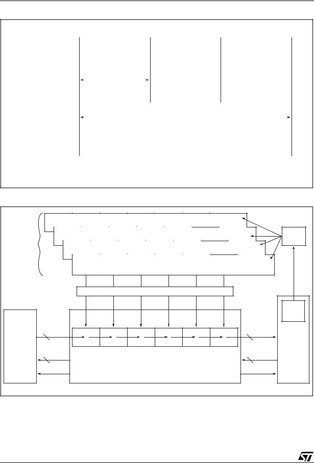
uPSD33xx
Figure 7. Comparison of uPSD33xx with Standard 8032 Performance
|
|
|
|
|
|
|
|
|
|
|
|
1-byte, 1-Cycle Instructions |
|
|
|||||||||||||||||||
|
|
|
|
|
|
Instruction A |
|
Instruction B |
|
|
Instruction C |
|
|
||||||||||||||||||||
|
|
|
|
|
|
|
|
|
|
|
|
|
|
|
|
|
|
|
|
|
|
|
|
|
|
|
|
|
|
|
|
|
|
Turbo uPSD33XX |
|
|
Execute Instruction and |
|
Execute Instruction and |
|
|
Execute Instruction and |
|
|
|||||||||||||||||||||||
|
Pre-Fetch Next Instruction |
Pre-Fetch Next Instruction |
|
Pre-Fetch Next Instruction |
|
|
|||||||||||||||||||||||||||
|
|
|
|
|
|
|
|
||||||||||||||||||||||||||
|
|
|
|
|
|
|
|
|
|
|
|
|
|
|
|
|
|
|
|
|
|
|
|
|
|
|
|
|
|
|
|
|
|
|
|
|
|
4 clocks (one machine cycle) |
|
one machine cycle |
|
|
one machine cycle |
|
|
||||||||||||||||||||||
MCU Clock |
|
|
|
|
|
|
|
|
|
|
|
|
|
|
|
|
|
|
|
|
|
|
|
|
|
|
|
|
|
|
|
|
|
|
|
|
|
|
|
|
|
|
|
|
|
|
|
|
|
|
|
|
|
|
|
|
|
|
|
|
|
|
|
|
|
||
|
|
|
|
|
|
|
|
|
|
|
|
|
|
|
|
|
|
|
|
|
|
|
|
|
|
|
|
|
|
|
|
||
|
|
|
|
|
|
|
|
|
|
|
|
|
|
|
|
|
|
|
|
|
|
|
|
|
|
|
|
|
|
|
|
|
|
|
|
|
|
|
|
|
|
|
|
|
|
|
|
12 clocks (one machine cycle) |
|
|
|
|
|
|
|
|
|
|
|
|
|||||||
|
|
|
|
|
|
|
|
|
|
|
|
|
|
|
|
|
|
|
|
|
|
|
|
|
|
|
|
|
|
|
|
|
|
|
|
|
|
|
|
|
|
|
|
|
|
|
|
|
Instruction A |
|
|
|
|
|
|
|
|
|
|
|
|
||||||
|
|
|
|
|
|
|
|
|
|
|
|
|
|
|
|
|
|
|
|
|
|
|
|
|
|
|
|
|
|
|
|
|
|
Standard 8032 |
|
|
|
Fetch Byte for Instruction A |
|
|
|
|
|
|
|
Execute Instruction A |
|
|
|||||||||||||||||||
|
|
|
|
|
|
|
|
and Fetch a Second Dummy Byte |
|
|
|||||||||||||||||||||||
|
|
|
|
|
|
|
|
|
|
|
|
|
|
|
|
|
|
|
|
|
|
||||||||||||
|
|
|
|
|
|
|
|
|
|
|
|
|
|
|
|
|
|
|
|
|
|
|
|
|
|
|
|
|
|
|
|
|
|
Dummy Byte is Ignored (wasted bus access)
Turbo uPSD33XX executes instructions A, B, and C in the same amount of time that a standard 8032 executes only instruction A.
AI08808
Figure 8. Instruction Pre-Fetch Queue and Branch Cache
|
Branch 4 |
Branch 4 |
Branch 4 |
Branch 4 |
Branch 4 |
Branch 4 |
|
Previous |
|
||||||||||||
|
Code |
|
Code |
|
Code |
|
Code |
|
|
Code |
|
|
Code |
|
|
Branch 4 |
|
||||
|
Branch 3 |
Branch 3 |
Branch 3 |
Branch 3 |
Branch 3 |
Branch 3 |
|
Previous |
Compare |
||||||||||||
Branch |
Code |
|
Code |
|
Code |
|
Code |
|
Code |
|
Code |
|
Branch 3 |
||||||||
Cache |
Branch 2 |
Branch 2 |
Branch 2 |
Branch 2 |
Branch 2 |
Branch 2 |
|
Previous |
|
||||||||||||
(BC) |
Code |
|
Code |
|
Code |
Code |
Code |
|
Code |
|
Branch 2 |
|
|||||||||
|
|
Branch 1 |
Branch 1 |
Branch 1 |
Branch 1 |
Branch 1 |
Branch 1 |
Previous |
|
||||||||||||
|
|
Branch 1 |
|
||||||||||||||||||
|
|
|
Code |
|
Code |
|
Code |
|
|
Code |
|
|
Code |
|
|
Code |
|
||||
|
|
|
|
|
|
|
|
|
|
|
Address |
|
|||||||||
|
|
|
|
|
|
|
|
|
|
|
|
|
|
|
|
|
|
|
|
|
|
|
|
|
|
|
|
|
Load on Branch Address Match |
|
|
|
|
|
|
|
|||||||
|
|
|
|
|
|
|
|
|
|
|
|
|
|
|
|
|
|
|
|
|
Current |
|
|
|
|
|
|
|
|
|
|
|
|
|
|
|
|
|
|
|
|
|
Branch |
|
|
|
|
|
|
|
|
|
|
|
|
|
|
|
|
|
|
|
|
|
Address |
|
Instruction |
|
|
|
|
|
|
|
|
|
|
|
|
|
|
|
|
|
|
Instruction |
|
|
Byte |
|
|
|
|
|
|
|
|
|
|
|
|
|
|
|
|
|
|
Byte |
8032 |
Program |
|
|
|
|
|
|
|
|
|
|
|
|
|
|
|
|
|
|
|
|
|
8 |
|
|
|
|
|
|
|
|
|
|
|
|
|
|
|
|
|
|
8 |
MCU |
|
Memory on |
|
|
|
|
|
|
|
|
|
|
|
|
|
|
|
|
|
|
|||
|
|
|
|
|
|
|
|
|
|
|
|
|
|
|
|
|
|
|
|
|
|
PSD Module |
Address |
|
|
|
|
|
|
6 Bytes of Instruction |
|
|
|
|
|
|
Address |
|
|||||
|
|
|
|
|
|
|
|
|
|
|
|
|
|
|
|
|
|
|
|
||
|
16 |
|
|
|
|
|
|
|
|
|
|
|
|
|
|
|
|
|
|
16 |
|
|
Wait |
|
|
|
|
Instruction Pre-Fetch Queue (PFQ) |
|
|
|
|
Stall |
|
|||||||||
|
|
|
|
|
|
|
|
|
|
|
|
|
|
|
|
|
|
|
|
|
AI08809 |
18/231 |
|
|
|
|
|
|
|
|
|
|
|
|
|
|
|
|
|
|
|
|
|

uPSD33xx
Pre-Fetch Queue (PFQ) and Branch Cache (BC)
The PFQ is always working to minimize the idle bus time inherent to 8032 MCU architecture, to eliminate wasted memory fetches, and to maximize memory bandwidth to the MCU. The PFQ does this by running asynchronously in relation to the MCU, looking ahead to pre-fetch code from program memory during any idle bus periods. Only necessary bytes will be fetched (no dummy fetches like standard 8032). The PFQ will queue up to six code bytes in advance of execution, which significantly optimizes sequential program performance. However, when program execution becomes non-sequential (program branch), a typical pre-fetch queue will empty itself and reload new code, causing the MCU to stall. The Turbo uPSD33xx diminishes this problem by using a Branch Cache with the PFQ. The BC is a four-way, fully associative cache, meaning that when a program branch occurs, it's branch destination address is compared simultaneously with four recent previous branch destinations stored in the BC. Each of the four cache entries contain up to six bytes of code related to a branch. If there is a hit (a match), then all six code bytes of the matching program branch are transferred immediately and simultaneously from the BC to the PFQ, and execution on that branch continues with minimal delay. This greatly reduces the chance that the MCU will stall from an empty PFQ, and improves performance in embedded control systems where it is quite common to branch and loop in relatively small code localities.
By default, the PFQ and BC are enabled after power-up or reset. The 8032 can disable the PFQ and BC at runtime if desired by writing to a specific SFR (BUSCON).
The memory in the PSD module operates with variable wait states depending on the value specified in the SFR named BUSCON. For example, a 5V uPSD33xx device operating at a 40MHz crystal frequency requires four memory wait states (equal to four MCU clocks). In this example, once the PFQ has one or more bytes of code, the wait states become transparent and a full 10 MIPS is achieved when the program stream consists of sequential one-byte, one machine-cycle instructions as shown in Figure 7., page 18 (transparent because a machine-cycle is four MCU clocks which equals the memory pre-fetch wait time that is also four MCU clocks). But it is also important to understand PFQ operation on multi-cycle instructions.
PFQ Example, Multi-cycle Instructions
Let us look at a string of two-byte, two-cycle instructions in Figure 9., page 20. There are three instructions executed sequentially in this example, instructions A, B, and C. Each of the time divisions in the figure is one machine-cycle of four clocks, and there are six phases to reference in this discussion. Each instruction is pre-fetched into the PFQ in advance of execution by the MCU. Prior to Phase 1, the PFQ has pre-fetched the two instruction bytes (A1 and A2) of instruction A. During Phase one, both bytes are loaded into the MCU execution unit. Also in Phase 1, the PFQ is prefetching the first byte (B1) of instruction B from program memory. In Phase 2, the MCU is processing Instruction A internally while the PFQ is pre-fetching the second byte (B2) of Instruction B. In Phase 3, both bytes of instruction B are loaded into the MCU execution unit and the PFQ begins to pre-fetch bytes for the third instruction C. In Phase 4 Instruction B is processed and the prefetching continues, eliminating idle bus cycles and feeding a continuous flow of operands and opcodes to the MCU execution unit.
The uPSD33xx MCU instructions are an exact 1/3 scale of all standard 8032 instructions with regard to number of cycles per instruction. Figure 10., page 20 shows the equivalent instruction sequence from the example above on a standard 8032 for comparison.
Aggregate Performance
The stream of two-byte, two-cycle instructions in Figure 9., page 20, running on a 40MHz, 5V, uPSD33xx will yield 5 MIPs. And we saw the stream of one-byte, one-cycle instructions in Figure 7., page 18, on the same MCU yield 10 MIPs. Effective performance will depend on a number of things: the MCU clock frequency; the mixture of instructions types (bytes and cycles) in the application; the amount of time an empty PFQ stalls the MCU (mix of instruction types and misses on Branch Cache); and the operating voltage. A 5V uPSD33xx device operates with four memory wait states, but a 3.3V device operates with five memory wait states yielding 8 MIPS peak compared to 10 MIPs peak for 5V device. The same number of wait states will apply to both program fetches and to data READ/WRITEs unless otherwise specified in the SFR named BUSCON.
In general, a 3X aggregate performance increase is expected over any standard 8032 application running at the same clock frequency.
19/231
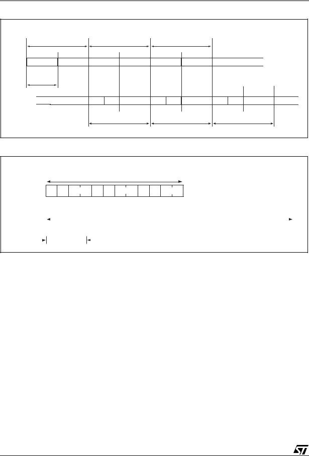
uPSD33xx
Figure 9. PFQ Operation on Multi-cycle Instructions
|
|
|
Three 2-byte, 2-cycle Instructions on uPSD33XX |
|
|
|
|
|||||
|
Pre-Fetch Inst A |
|
Pre-Fetch Inst B |
|
Pre-Fetch Inst C |
|
|
|
|
|||
PFQ |
Inst A, Byte 1 |
Inst A, Byte 2 |
Inst B, Byte 1 |
Inst B, Byte 2 |
Inst C, Byte 1 |
Inst C, Byte 2 |
Continue to Pre-Fetch |
|
||||
|
4-clock |
|
|
|
|
|
|
|
|
|
|
|
|
Macine Cycle |
|
|
|
|
|
|
|
|
|
|
|
|
|
|
Phase 1 |
Phase 2 |
Phase 3 |
Phase 4 |
Phase 5 |
Phase 6 |
|
|||
MCU |
Previous Instruction |
A1 |
A2 |
Process A |
B1 |
B2 |
Process B |
C1 |
C2 |
Process C |
Next Inst |
|
Execution |
|
|
|
|
|
|
|
|
|
|
|
|
|
|
|
|
Instruction A |
|
Instruction B |
|
Instruction C |
|
|||
|
|
|
|
|
|
|
|
|
|
|
|
AI08810 |
Figure 10. uPSD33xx Multi-cycle Instructions Compared to Standard 8032
Three 2-byte, 2-cycle Instructions, uPSD33XX vs. Standard 8032
24 Clocks Total (4 clocks per cycle) uPSD33XX A1 A2 Inst A B1 B2 Inst B C1 C2 Inst C


 1 Cycle
|
|
|
|
|
|
|
|
|
|
72 Clocks (12 clocks per cycle) |
|
|||||||
|
|
|
|
|
|
|
|
|
|
|
|
|
|
|
|
|
||
Std 8032 |
Byte 1 |
Byte 2 |
|
Process Inst A |
Byte 1 |
Byte 2 |
Process Inst B |
Byte 1 |
Byte 2 |
Process Inst C |
|
|||||||
|
|
|
|
|
|
|
|
|
|
|
|
|
|
|
|
|
|
|
|
|
|
|
|
|
|
|
1 Cycle |
|
|||||||||
|
|
|
|
|
|
|
|
|||||||||||
AI08811
20/231
uPSD33xx
MCU MODULE DISCRIPTION
This section provides a detail description of the MCU Module system functions and peripherals, including:
■8032 MCU Registers
■Special Function Registers
■8032 Addressing Modes
■uPSD33xx Instruction Set Summary
■Dual Data Pointers
■Debug Unit
■Interrupt System
■MCU Clock Generation
■Power Saving Modes
■Oscillator and External Components
8032 MCU REGISTERS
The uPSD33xx has the following 8032 MCU core registers, also shown in Figure 11.
Figure 11. 8032 MCU Registers
|
A |
Accumulator |
|
|
B Register |
|
B |
|
|
|
Stack Pointer |
|
SP |
|
|
|
Program Counter |
PCH |
PCL |
|
|
|
Program Status Word |
|
PSW |
|
|
|
General Purpose |
|
R0-R7 |
Register (Bank0-3) |
|
|
|
DPTR(DPH) |
DPTR(DPL) |
Data Pointer Register |
AI06636
Stack Pointer (SP)
The SP is an 8-bit register which holds the current location of the top of the stack. It is incremented before a value is pushed onto the stack, and decremented after a value is popped off the stack. The SP is initialized to 07h after reset. This causes the stack to begin at location 08h (top of stack). To avoid overlapping conflicts, the user must initialize the top of the stack to 20h if all four banks of registers R0 - R7 are used, and the user must initialize the top of stack to 30h if all of the 8032 bit memory locations are used.
Data Pointer (DPTR)
DPTR is a 16-bit register consisting of two 8-bit registers, DPL and DPH. The DPTR Register is used as a base register to create an address for indirect jumps, table look-up operations, and for external data transfers (XDATA). When not used for addressing, the DPTR Register can be used as a general purpose 16-bit data register.
■I/O Ports
■MCU Bus Interface
■Supervisory Functions
■Standard 8032 Timer/Counters
■Serial UART Interfaces
■IrDA Interface
■I2C Interface
■SPI Interface
■Analog to Digital Converter
■Programmable Counter Array (PCA)
Note: A full description of the 8032 instruction set may be found in the uPSD33xx Programmers Guide.
Very frequently, the DPTR Register is used to access XDATA using the External Direct addressing mode. The uPSD33xx has a special set of SFR registers (DPTC, DPTM) to control a secondary DPTR Register to speed memory-to-memory XDATA transfers. Having dual DPTR Registers allows rapid switching between source and destination addresses (see details in DUAL DATA POINTERS, page 37).
Program Counter (PC)
The PC is a 16-bit register consisting of two 8-bit registers, PCL and PCH. This counter indicates the address of the next instruction in program memory to be fetched and executed. A reset forces the PC to location 0000h, which is where the reset jump vector is stored.
Accumulator (ACC)
This is an 8-bit general purpose register which holds a source operand and receives the result of arithmetic operations. The ACC Register can also be the source or destination of logic and data movement operations. For MUL and DIV instructions, ACC is combined with the B Register to hold 16-bit operands. The ACC is referred to as “A” in the MCU instruction set.
B Register (B)
The B Register is a general purpose 8-bit register for temporary data storage and also used as a 16bit register when concatenated with the ACC Register for use with MUL and DIV instructions.
21/231
uPSD33xx
General Purpose Registers (R0 - R7)
There are four banks of eight general purpose 8- bit registers (R0 - R7), but only one bank of eight registers is active at any given time depending on the setting in the PSW word (described next). R0 - R7 are generally used to assist in manipulating values and moving data from one memory location to another. These register banks physically reside in the first 32 locations of 8032 internal DATA SRAM, starting at address 00h. At reset, only the first bank of eight registers is active (addresses 00h to 07h), and the stack begins at address 08h.
Program Status Word (PSW)
The PSW is an 8-bit register which stores several important bits, or flags, that are set and cleared by many 8032 instructions, reflecting the current state of the MCU core. Figure 12., page 22 shows the individual flags.
Carry Flag (CY). This flag is set when the last arithmetic operation that was executed results in a carry (addition) or borrow (subtraction). It is cleared by all other arithmetic operations. The CY flag is also affected by Shift and Rotate Instructions.
Auxiliary Carry Flag (AC). This flag is set when the last arithmetic operation that was executed results in a carry into (addition) or borrow from (subtraction) the high-order nibble. It is cleared by all other arithmetic operations.
Figure 12. Program Status Word (PSW) Register
General Purpose Flag (F0). This is a bit-addres- sable, general-purpose flag for use under software control.
Register Bank Select Flags (RS1, RS0). These bits select which bank of eight registers is used during R0 - R7 register accesses (see Table 4)
Overflow Flag (OV). The OV flag is set when: an ADD, ADDC, or SUBB instruction causes a sign change; a MUL instruction results in an overflow (result greater than 255); a DIV instruction causes a divide-by-zero condition. The OV flag is cleared by the ADD, ADDC, SUBB, MUL, and DIV instructions in all other cases. The CLRV instruction will clear the OV flag at any time.
Parity Flag (P). The P flag is set if the sum of the eight bits in the Accumulator is odd, and P is cleared if the sum is even.
Table 4. .Register Bank Select Addresses
RS1 |
RS0 |
Register |
8032 Internal |
|
Bank |
DATA Address |
|||
|
|
|||
|
|
|
|
|
0 |
0 |
0 |
00h - 07h |
|
|
|
|
|
|
0 |
1 |
1 |
08h - 0Fh |
|
|
|
|
|
|
1 |
0 |
2 |
10h - 17h |
|
|
|
|
|
|
1 |
1 |
3 |
18h - 1Fh |
|
|
|
|
|
MSB |
LSB |
|||
|
|
|
|
|
PSW |
CY |
AC FO RS1 RS0 OV |
P |
Reset Value 00h |
Carry Flag |
|
Parity Flag |
||
Auxillary Carry Flag |
|
Bit not assigned |
||
General Purpose Flag |
|
Overflow Flag |
||
|
|
Register Bank Select Flags |
|
|
|
|
(to select Bank0-3) |
|
AI06639 |
|
|
|
|
|
|
|
|
|
|
22/231

uPSD33xx
SPECIAL FUNCTION REGISTERS (SFR)
A group of registers designated as Special Function Register (SFR) is shown in Table 5., page 24. SFRs control the operating modes of the MCU core and also control the peripheral interfaces and I/O pins on the MCU Module. The SFRs can be accessed only by using the Direct Addressing method within the address range from 80h to FFh of internal 8032 SRAM. Sixteen addresses in SFR address space are both byteand bit-addressable. The bit-addressable SFRs are noted in Table 5.
86 of a possible 128 SFR addresses are occupied. The remaining unoccupied SFR addresses (designated as “RESERVED” in Table5) should not be written. Reading unoccupied locations will return an undefined value.
Note: There is a separate set of control registers for the PSD Module, designated as csiop, and they are described in the PSD MODULE, page 133. The I/O pins, PLD, and other functions on the PSD Module are NOT controlled by SFRs.
SFRs are categorized as follows:
■MCU core registers:
IP, A, B, PSW, SP, DPTL, DPTH, DPTC, DPTM
■MCU Module I/O Port registers:
P1, P3, P4, P1SFS0, P1SFS1, P3SFS, P4SFS0, P4SFS1
■Standard 8032 Timer registers
TCON, TMOD, T2CON, TH0, TH1, TH2, TL0, TL1, TL2, RCAP2L, RCAP2H
■Standard Serial Interfaces (UART)
SCON0, SBUF0, SCON1, SBUF1
■Power, clock, and bus timing registers
PCON, CCON0, BUSCON
■Hardware watchdog timer registers
WDKEY, WDRST
■Interrupt system registers
IP, IPA, IE, IEA
■Prog. Counter Array (PCA) control registers
PCACL0, PCACH0, PCACON0, PCASTA, PCACL1, PCACH1, PCACON1, CCON2, CCON3
■PCA capture/compare and PWM registers
CAPCOML0, CAPCOMH0, TCMMODE0, CAPCOML1, CAPCOMH1, TCMMODE2, CAPCOML2, CAPCOMH2, TCMMODE2, CAPCOML3, CAPCOMH3, TCMMODE3, CAPCOML4, CAPCOMH4, TCMMODE4, CAPCOML5, CAPCOMH5, TCMMODE5, PWMF0, PMWF1
■SPI interface registers
SPICLKD, SPISTAT, SPITDR, SPIRDR, SPICON0, SPICON1
■I2C interface registers
S1SETUP, S1CON, S1STA, S1DAT, S1ADR
■Analog to Digital Converter registers
ACON, ADCPS, ADAT0, ADAT1
■IrDA interface register
IRDACON
23/231

uPSD33xx
Table 5. SFR Memory Map with Direct Address and Reset Value
SFR |
SFR |
|
|
|
|
|
Bit Name and <Bit Address> |
|
|
|
Reset |
Reg. |
||||||
Addr |
|
|
|
|
|
|
|
|
|
|
|
|
|
|
Value |
Descr. |
||
Name |
7 |
6 |
|
5 |
4 |
|
3 |
2 |
|
1 |
|
0 |
||||||
(hex) |
|
|
|
|
(hex) |
with Link |
||||||||||||
|
|
|
|
|
|
|||||||||||||
|
|
|
|
|
|
|
|
|
|
|
|
|
|
|
|
|
|
|
80 |
|
|
|
|
|
|
|
RESERVED |
|
|
|
|
|
|
|
|
||
|
|
|
|
|
|
|
|
|
|
|
|
|
|
|
|
|
|
|
|
|
|
|
|
|
|
|
|
|
|
|
|
|
|
|
|
|
Stack |
81 |
SP |
|
|
|
|
|
SP[7:0] |
|
|
|
|
|
|
|
07 |
Pointer |
||
|
|
|
|
|
|
|
|
|
|
|
|
(SP), page |
||||||
|
|
|
|
|
|
|
|
|
|
|
|
|
|
|
|
|
|
|
|
|
|
|
|
|
|
|
|
|
|
|
|
|
|
|
|
|
21 |
|
|
|
|
|
|
|
|
|
|
|
|
|
|
|
|
|||
82 |
DPL |
|
|
|
|
|
DPL[7:0] |
|
|
|
|
|
|
00 |
Data |
|||
|
|
|
|
|
|
|
|
|
|
|
|
|
|
|
|
|
|
Pointer |
|
|
|
|
|
|
|
|
|
|
|
|
|
|
|
|
|
|
|
83 |
DPH |
|
|
|
|
|
DPH[7:0] |
|
|
|
|
|
|
00 |
(DPTR), p |
|||
|
|
|
|
|
|
|
|
|
|
|
age 21 |
|||||||
|
|
|
|
|
|
|
|
|
|
|
|
|
|
|
|
|
|
|
|
|
|
|
|
|
|
|
|
|
|
|
|
|
|
|
|
|
|
84 |
|
|
|
|
|
|
|
RESERVED |
|
|
|
|
|
|
|
|
||
|
|
|
|
|
|
|
|
|
|
|
|
|
|
|
|
|
|
|
85 |
|
|
|
|
|
|
|
|
|
|
|
|
|
|
|
|
|
Table |
DPTC |
– |
AT |
– |
– |
|
– |
|
|
DPSEL[2:0] |
|
00 |
13., page |
||||||
|
|
|
|
|
|
|
|
|
|
|
|
|
|
|
|
|
|
37 |
|
|
|
|
|
|
|
|
|
|
|
|
|
|
|
|
|
|
|
86 |
|
|
|
|
|
|
|
|
|
|
|
|
|
|
|
|
|
Table |
DPTM |
– |
– |
– |
– |
|
MD1[1:0] |
MD0[1:0] |
00 |
14., page |
|||||||||
|
|
|
|
|
|
|
|
|
|
|
|
|
|
|
|
|
|
38 |
|
|
|
|
|
|
|
|
|
|
|
|
|
|
|
|
|
|
|
87 |
|
|
|
|
|
|
|
|
|
|
|
|
|
|
|
|
|
Table |
PCON |
SMOD0 |
SMOD1 |
– |
POR |
|
RCLK1 |
TCLK1 |
PD |
|
IDLE |
00 |
24., page |
||||||
|
|
|
|
|
|
|
|
|
|
|
|
|
|
|
|
|
|
50 |
|
|
|
|
|
|
|
|
|
|
|
|
|
|
|
|
|
|
|
88(1) |
|
|
TF1 |
TR1 |
TF0 |
TR0 |
|
IE1 |
IT1 |
IE0 |
|
IT0 |
|
Table |
||||
TCON |
|
|
00 |
39., page |
||||||||||||||
<8Fh> |
<8Eh> |
<8Dh> |
<8Ch> |
|
<8Bh> |
<8Ah> |
<89h> |
|
<88h> |
|||||||||
|
|
|
|
|
|
70 |
||||||||||||
|
|
|
|
|
|
|
|
|
|
|
|
|
|
|
|
|
|
|
|
|
|
|
|
|
|
|
|
|
|
|
|
|
|
|
|
|
|
89 |
|
|
|
|
|
|
|
|
|
|
|
|
|
|
|
|
|
Table |
TMOD |
GATE |
C/T |
|
M1 |
M0 |
|
GATE |
C/T |
M1 |
|
M0 |
00 |
40., page |
|||||
|
|
|
|
|
|
|
|
|
|
|
|
|
|
|
|
|
|
72 |
|
|
|
|
|
|
|
|
|
|
|
|
|
|
|
|
|
|
|
8A |
TL0 |
|
|
|
|
|
TL0[7:0] |
|
|
|
|
|
|
|
00 |
Standard |
||
|
|
|
|
|
|
|
|
|
|
|
|
|
|
|
|
|
|
|
8B |
TL1 |
|
|
|
|
|
TL1[7:0] |
|
|
|
|
|
|
|
00 |
|||
|
|
|
|
|
|
|
|
|
|
|
|
Timer |
||||||
|
|
|
|
|
|
|
|
|
|
|
|
|
|
|
|
|
|
|
8C |
TH0 |
|
|
|
|
|
TH0[7:0] |
|
|
|
|
|
|
00 |
SFRs, pag |
|||
|
|
|
|
|
|
|
|
|
|
|
e 69 |
|||||||
|
|
|
|
|
|
|
|
|
|
|
|
|
|
|
|
|
|
|
8D |
TH1 |
|
|
|
|
|
TH1[7:0] |
|
|
|
|
|
|
00 |
||||
|
|
|
|
|
|
|
|
|
|
|
|
|||||||
|
|
|
|
|
|
|
|
|
|
|
|
|
|
|
|
|
|
|
8E |
|
|
|
|
|
|
|
|
|
|
|
|
|
|
|
|
|
Table |
P1SFS0 |
|
|
|
|
|
P1SFS0[7:0] |
|
|
|
|
|
|
00 |
29., page |
||||
|
|
|
|
|
|
|
|
|
|
|
|
|
|
|
|
|
|
60 |
|
|
|
|
|
|
|
|
|
|
|
|
|
|
|
|
|
|
|
8F |
|
|
|
|
|
|
|
|
|
|
|
|
|
|
|
|
|
Table |
P1SFS1 |
|
|
|
|
|
P1SFS1[7:0] |
|
|
|
|
|
|
00 |
30., page |
||||
|
|
|
|
|
|
|
|
|
|
|
|
|
|
|
|
|
|
60 |
|
|
|
|
|
|
|
|
|
|
|
|
|
|
|
|
|
|
|
90(1) |
|
|
P1.7 |
P1.6 |
P1.5 |
P1.4 |
|
P1.3 |
P1.2 |
P1.1 |
|
P1.0 |
|
Table |
||||
P1 |
|
|
FF |
25., page |
||||||||||||||
<97h> |
<96h> |
<95h> |
<94h> |
|
<93h> |
<92h> |
<91h> |
|
<90h> |
|||||||||
|
|
|
|
|
|
57 |
||||||||||||
|
|
|
|
|
|
|
|
|
|
|
|
|
|
|
|
|
|
|
|
|
|
|
|
|
|
|
|
|
|
|
|
|
|
|
|
|
|
91 |
|
|
|
|
|
|
|
|
|
|
|
|
|
|
|
|
|
Table |
P3SFS |
|
|
|
|
|
P3SFS[7:0] |
|
|
|
|
|
|
00 |
28., page |
||||
|
|
|
|
|
|
|
|
|
|
|
|
|
|
|
|
|
|
60 |
|
|
|
|
|
|
|
|
|
|
|
|
|
|
|
|
|
|
|
92 |
|
|
|
|
|
|
|
|
|
|
|
|
|
|
|
|
|
Table |
P4SFS0 |
|
|
|
|
|
P4SFS0[7:0] |
|
|
|
|
|
|
00 |
32., page |
||||
|
|
|
|
|
|
|
|
|
|
|
|
|
|
|
|
|
|
61 |
|
|
|
|
|
|
|
|
|
|
|
|
|
|
|
|
|
|
|
93 |
|
|
|
|
|
|
|
|
|
|
|
|
|
|
|
|
|
Table |
P4SFS1 |
|
|
|
|
|
P4SFS1[7:0] |
|
|
|
|
|
|
00 |
33., page |
||||
|
|
|
|
|
|
|
|
|
|
|
|
|
|
|
|
|
|
61 |
|
|
|
|
|
|
|
|
|
|
|
|
|
|
|
|
|
|
|
24/231 |
|
|
|
|
|
|
|
|
|
|
|
|
|
|
|
|
|
|

uPSD33xx
SFR |
SFR |
|
|
|
Bit Name and <Bit Address> |
|
|
|
Reset |
Reg. |
|||
Addr |
|
|
|
|
|
|
|
|
|
Value |
Descr. |
||
Name |
7 |
6 |
5 |
4 |
3 |
2 |
1 |
|
0 |
||||
(hex) |
|
(hex) |
with Link |
||||||||||
|
|
|
|||||||||||
|
|
|
|
|
|
|
|
|
|
|
|
|
|
94 |
|
|
|
|
|
|
|
|
|
|
|
|
Table |
ADCPS |
– |
– |
– |
– |
ADCCE |
ADCPS[2:0] |
|
00 |
64., page |
||||
|
|
|
|
|
|
|
|
|
|
|
|
|
122 |
|
|
|
|
|
|
|
|
|
|
|
|
|
|
95 |
|
|
|
|
|
|
|
|
|
|
|
|
Table |
ADAT0 |
|
|
|
ADATA[7:0] |
|
|
|
|
00 |
65., page |
|||
|
|
|
|
|
|
|
|
|
|
|
|
|
122 |
|
|
|
|
|
|
|
|
|
|
|
|
|
|
96 |
|
|
|
|
|
|
|
|
|
|
|
|
Table |
ADAT1 |
– |
– |
– |
– |
– |
– |
ADATA[9:8] |
00 |
66., page |
||||
|
|
|
|
|
|
|
|
|
|
|
|
|
122 |
|
|
|
|
|
|
|
|
|
|
|
|
|
|
97 |
|
|
|
|
|
|
|
|
|
|
|
|
Table |
ACON |
AINTF |
AINTEN |
ADEN |
|
ADS[2:0] |
|
ADST |
|
ADSF |
00 |
63., page |
||
|
|
|
|
|
|
|
|
|
|
|
|
|
121 |
|
|
|
|
|
|
|
|
|
|
|
|
|
|
98(1) |
|
|
SM0 |
SM1 |
SM2 |
REN |
TB8 |
RB8 |
TI |
|
RI |
|
Table |
SCON0 |
|
00 |
45., page |
||||||||||
<9Fh> |
<9Eh> |
<9Dh> |
<9Ch> |
<9Bh> |
<9Ah> |
<99h> |
|
<9h8> |
|||||
|
|
|
|
|
82 |
||||||||
|
|
|
|
|
|
|
|
|
|
|
|
|
|
|
|
|
|
|
|
|
|
|
|
|
|
|
|
99 |
|
|
|
|
|
|
|
|
|
|
|
|
Figure |
SBUF0 |
|
|
|
SBUF0[7:0] |
|
|
|
|
00 |
25., page |
|||
|
|
|
|
|
|
|
|
|
|
|
|
|
79 |
|
|
|
|
|
|
|
|
|
|
|
|
|
|
9A |
|
|
|
|
|
RESERVED |
|
|
|
|
|
|
|
|
|
|
|
|
|
|
|
|
|
|
|
|
|
9B |
|
|
|
|
|
RESERVED |
|
|
|
|
|
|
|
|
|
|
|
|
|
|
|
|
|
|
|
|
|
9C |
|
|
|
|
|
RESERVED |
|
|
|
|
|
|
|
|
|
|
|
|
|
|
|
|
|
|
|
|
|
9D |
|
|
|
|
|
|
|
|
|
|
|
|
Table |
BUSCON |
EPFQ |
EBC |
WRW1 |
WRW0 |
RDW1 |
RDW0 |
CW1 |
|
CW0 |
EB |
35., page |
||
|
|
|
|
|
|
|
|
|
|
|
|
|
63 |
|
|
|
|
|
|
|
|
|
|
|
|
|
|
9E |
|
|
|
|
|
RESERVED |
|
|
|
|
|
|
|
|
|
|
|
|
|
|
|
|
|
|
|
|
|
9F |
|
|
|
|
|
RESERVED |
|
|
|
|
|
|
|
|
|
|
|
|
|
|
|
|
|
|
|
|
|
A0 |
|
|
|
|
|
RESERVED |
|
|
|
|
|
|
|
|
|
|
|
|
|
|
|
|
|
|
|
|
|
A1 |
|
|
|
|
|
RESERVED |
|
|
|
|
|
|
|
|
|
|
|
|
|
|
|
|
|
|
|
|
|
A2 |
|
|
|
|
|
|
|
|
|
|
|
|
Table |
PCACL0 |
|
|
|
PCACL0[7:0] |
|
|
|
|
00 |
67., page |
|||
|
|
|
|
|
|
|
|
|
|
|
|
|
124 |
|
|
|
|
|
|
|
|
|
|
|
|
|
|
A3 |
|
|
|
|
|
|
|
|
|
|
|
|
Table |
PCACH0 |
|
|
|
PCACH0[7:0] |
|
|
|
|
00 |
67., page |
|||
|
|
|
|
|
|
|
|
|
|
|
|
|
124 |
|
|
|
|
|
|
|
|
|
|
|
|
|
|
A4 |
|
|
|
|
|
|
|
|
|
|
|
|
Table |
PCACON0 |
EN_ALL |
EN_PCA |
EOVF1 |
PCA_IDL |
– |
– |
CLK_SEL[1:0] |
00 |
70., page |
||||
|
|
|
|
|
|
|
|
|
|
|
|
|
129 |
|
|
|
|
|
|
|
|
|
|
|
|
|
|
A5 |
|
|
|
|
|
|
|
|
|
|
|
|
Table |
PCASTA |
OVF1 |
INTF5 |
INTF4 |
INTF3 |
OVF0 |
INTF2 |
INTF1 |
|
INTF0 |
00 |
72., page |
||
|
|
|
|
|
|
|
|
|
|
|
|
|
131 |
|
|
|
|
|
|
|
|
|
|
|
|
|
|
A6 |
|
|
|
|
|
|
|
|
|
|
|
|
Table |
WDTRST |
|
|
|
WDTRST[7:0] |
|
|
|
|
00 |
38., page |
|||
|
|
|
|
|
|
|
|
|
|
|
|
|
68 |
|
|
|
|
|
|
|
|
|
|
|
|
|
|
A7 |
|
|
|
|
|
|
|
|
|
|
|
|
Table |
IEA |
EADC |
ESPI |
EPCA |
ES1 |
– |
– |
EI2C |
|
– |
00 |
18., page |
||
|
|
|
|
|
|
|
|
|
|
|
|
|
44 |
|
|
|
|
|
|
|
|
|
|
|
|
|
|
25/231

uPSD33xx
SFR |
SFR |
|
|
|
Bit Name and <Bit Address> |
|
|
Reset |
Reg. |
||||
Addr |
|
|
|
|
|
|
|
|
|
Value |
Descr. |
||
Name |
7 |
6 |
5 |
|
4 |
3 |
2 |
1 |
0 |
||||
(hex) |
|
(hex) |
with Link |
||||||||||
|
|
|
|||||||||||
|
|
|
|
|
|
|
|
|
|
|
|
|
|
A8(1) |
IE |
EA |
– |
ET2 |
|
ES0 |
ET1 |
EX1 |
ET0 |
EX0 |
|
Table |
|
|
00 |
17., page |
|||||||||||
<AFh> |
<ADh> |
|
<ACh> |
<ABh> |
<AAh> |
<A9h> |
<A8h> |
||||||
|
|
|
|
|
|
43 |
|||||||
|
|
|
|
|
|
|
|
|
|
|
|
|
|
|
|
|
|
|
|
|
|
|
|
|
|
|
|
A9 |
TCMMODE |
EINTF |
E_COMP |
CAP_PE |
|
CAP_NE |
MATCH |
TOGGLE |
PWM[1:0] |
00 |
|
||
|
0 |
|
|
|
|
|
|
|
|
|
|
|
|
|
|
|
|
|
|
|
|
|
|
|
|
|
Table |
AA |
TCMMODE |
|
|
|
|
|
|
|
|
|
|
||
EINTF |
E_COMP |
CAP_PE |
|
CAP_NE |
MATCH |
TOGGLE |
PWM[1:0] |
00 |
73., page |
||||
|
1 |
|
|
|
|
|
|
|
|
|
|
|
132 |
AB |
TCMMODE |
EINTF |
E_COMP |
CAP_PE |
|
CAP_NE |
MATCH |
TOGGLE |
PWM[1:0] |
00 |
|
||
|
2 |
|
|
|
|
|
|
|
|
|
|
|
|
|
|
|
|
|
|
|
|
|
|
|
|
|
|
AC |
CAPCOML |
|
|
|
CAPCOML0[7:0] |
|
|
|
00 |
Table |
|||
0 |
|
|
|
|
|
|
|
||||||
|
|
|
|
|
|
|
|
|
|
|
|
||
|
|
|
|
|
|
|
|
|
|
|
|
|
67., page |
|
CAPCOMH |
|
|
|
|
|
|
|
|
|
|
||
AD |
|
|
|
CAPCOMH0[7:0] |
|
|
|
00 |
124 |
||||
0 |
|
|
|
|
|
|
|
|
|||||
|
|
|
|
|
|
|
|
|
|
|
|
|
|
|
|
|
|
|
|
|
|
|
|
|
|
|
|
AE |
|
|
|
|
|
|
|
|
|
|
|
|
Table |
WDTKEY |
|
|
|
|
WDTKEY[7:0] |
|
|
|
55 |
37., page |
|||
|
|
|
|
|
|
|
|
|
|
|
|
|
68 |
|
|
|
|
|
|
|
|
|
|
|
|
|
|
AF |
CAPCOML |
|
|
|
|
|
|
|
|
|
|
Table |
|
|
|
|
CAPCOML1[7:0] |
|
|
|
00 |
67., page |
|||||
1 |
|
|
|
|
|
|
|
||||||
|
|
|
|
|
|
|
|
|
|
|
|
124 |
|
|
|
|
|
|
|
|
|
|
|
|
|
|
|
|
|
|
|
|
|
|
|
|
|
|
|
|
|
B0(1) |
|
|
P3.7 |
P3.6 |
P3.5 |
|
P3.4 |
P3.3 |
P3.2 |
P3.1 |
P3.0 |
|
Table |
P3 |
|
FF |
26., page |
||||||||||
<B7h> |
<B6h> |
<B5h> |
|
<B4h> |
<B3h> |
<B2h> |
<B1h> |
<B0h> |
|||||
|
|
|
|
|
58 |
||||||||
|
|
|
|
|
|
|
|
|
|
|
|
|
|
|
|
|
|
|
|
|
|
|
|
|
|
|
|
B1 |
CAPCOMH |
|
|
|
CAPCOMH1[7:0] |
|
|
|
00 |
|
|||
1 |
|
|
|
|
|
|
|
|
|||||
|
|
|
|
|
|
|
|
|
|
|
|
|
|
|
|
|
|
|
|
|
|
|
|
|
|
|
|
B2 |
CAPCOML |
|
|
|
CAPCOML2[7:0] |
|
|
|
00 |
Table |
|||
2 |
|
|
|
|
|
|
|
||||||
|
|
|
|
|
|
|
|
|
|
|
|
67., page |
|
|
|
|
|
|
|
|
|
|
|
|
|
|
|
B3 |
CAPCOMH |
|
|
|
CAPCOMH2[7:0] |
|
|
|
00 |
124 |
|||
|
|
|
|
|
|
|
|||||||
2 |
|
|
|
|
|
|
|
|
|||||
|
|
|
|
|
|
|
|
|
|
|
|
|
|
|
|
|
|
|
|
|
|
|
|
|
|
||
B4 |
PWMF0 |
|
|
|
|
PWMF0[7:0] |
|
|
|
00 |
|
||
|
|
|
|
|
|
|
|
|
|
|
|
|
|
B5 |
|
|
|
|
|
|
RESERVED |
|
|
|
|
|
|
|
|
|
|
|
|
|
|
|
|
|
|
|
|
B6 |
|
|
|
|
|
|
RESERVED |
|
|
|
|
|
|
|
|
|
|
|
|
|
|
|
|
|
|
|
|
B7 |
|
|
|
|
|
|
|
|
|
|
|
|
Table |
IPA |
PADC |
PSPI |
PPCA |
|
PS1 |
– |
– |
PI2C |
– |
00 |
20., page |
||
|
|
|
|
|
|
|
|
|
|
|
|
|
45 |
|
|
|
|
|
|
|
|
|
|
|
|
|
|
B8(1) |
|
|
|
|
PT2 |
|
PS0 |
PT1 |
PX1 |
PT0 |
PX0 |
|
Table |
IP |
– |
– |
|
00 |
19., page |
||||||||
<BDh> |
|
<BCh> |
<BBh> |
<BAh> |
<B9h> |
<B8h> |
|||||||
|
|
|
|
|
|
|
44 |
||||||
|
|
|
|
|
|
|
|
|
|
|
|
|
|
|
|
|
|
|
|
|
|
|
|
|
|
|
|
B9 |
|
|
|
|
|
|
RESERVED |
|
|
|
|
|
|
|
|
|
|
|
|
|
|
|
|
|
|
|
|
BA |
PCACL1 |
|
|
|
|
PCACL1[7:0] |
|
|
|
00 |
Table |
||
|
|
|
|
|
|
|
|
|
|
|
|
|
67., page |
BB |
PCACH1 |
|
|
|
|
PCACH1[7:0] |
|
|
|
00 |
|||
|
|
|
|
|
|
|
124 |
||||||
|
|
|
|
|
|
|
|
|
|
|
|
|
|
BC |
|
|
|
|
|
|
|
|
|
|
|
|
Table |
PCACON1 |
– |
EN_PCA |
EOVF1 |
|
PCA_IDL |
– |
– |
CLK_SEL[1:0] |
00 |
71., page |
|||
|
|
|
|
|
|
|
|
|
|
|
|
|
130 |
|
|
|
|
|
|
|
|
|
|
|
|
|
|
26/231

uPSD33xx
SFR |
SFR |
|
|
|
Bit Name and <Bit Address> |
|
|
|
|
Reset |
Reg. |
||||
Addr |
|
|
|
|
|
|
|
|
|
|
|
Value |
Descr. |
||
Name |
7 |
6 |
5 |
|
4 |
3 |
2 |
1 |
|
0 |
|||||
(hex) |
|
|
(hex) |
with Link |
|||||||||||
|
|
|
|
||||||||||||
|
|
|
|
|
|
|
|
|
|
|
|
|
|
||
BD |
TCMMODE |
EINTF |
E_COMP |
CAP_PE |
|
CAP_NE |
MATCH |
TOGGLE |
PWM[1:0] |
00 |
|
||||
|
3 |
|
|
|
|
|
|
|
|
|
|
|
|
|
|
|
|
|
|
|
|
|
|
|
|
|
|
|
|
|
Table |
BE |
TCMMODE |
|
|
|
|
|
|
|
|
|
|
|
|
||
EINTF |
E_COMP |
CAP_PE |
|
CAP_NE |
MATCH |
TOGGLE |
PWM[1:0] |
00 |
73., page |
||||||
|
4 |
|
|
|
|
|
|
|
|
|
|
|
|
|
132 |
BF |
TCMMODE |
EINTF |
E_COMP |
CAP_PE |
|
CAP_NE |
MATCH |
TOGGLE |
PWM[1:0] |
00 |
|
||||
|
5 |
|
|
|
|
|
|
|
|
|
|
|
|
|
|
C0(1) |
|
|
P4.7 |
P4.6 |
P4.5 |
|
P4.4 |
P4.3 |
P4.2 |
P4.1 |
P4.0 |
|
Table |
||
P4 |
|
FF |
27., page |
||||||||||||
<C7h> |
<C6h> |
<C5h> |
|
<C4h> |
<C3h> |
<C2h> |
<C1h> |
<C0h> |
|||||||
|
|
|
|
|
58 |
||||||||||
|
|
|
|
|
|
|
|
|
|
|
|
|
|
|
|
|
|
|
|
|
|
|
|
|
|
|
|
|
|
|
|
C1 |
CAPCOML |
|
|
|
CAPCOML3[7:0] |
|
|
|
|
|
00 |
|
|||
3 |
|
|
|
|
|
|
|
|
|
|
|||||
|
|
|
|
|
|
|
|
|
|
|
|
|
|
|
|
|
|
|
|
|
|
|
|
|
|
|
|
|
|
|
|
C2 |
CAPCOMH |
|
|
CAPCOMH3[7:0] |
|
|
|
|
|
00 |
|
||||
3 |
|
|
|
|
|
|
|
|
|
||||||
|
|
|
|
|
|
|
|
|
|
|
|
|
|
|
|
|
|
|
|
|
|
|
|
|
|
|
|
|
|
|
|
C3 |
CAPCOML |
|
|
|
CAPCOML4[7:0] |
|
|
|
|
|
00 |
|
|||
4 |
|
|
|
|
|
|
|
|
|
|
|||||
|
|
|
|
|
|
|
|
|
|
|
|
|
|
Table |
|
|
|
|
|
|
|
|
|
|
|
|
|
|
|
|
|
C4 |
CAPCOMH |
|
|
CAPCOMH4[7:0] |
|
|
|
|
|
00 |
67., page |
||||
4 |
|
|
|
|
|
|
|
|
124 |
||||||
|
|
|
|
|
|
|
|
|
|
|
|
|
|
||
|
|
|
|
|
|
|
|
|
|
|
|
|
|
|
|
C5 |
CAPCOML |
|
|
|
CAPCOML5[7:0] |
|
|
|
|
|
00 |
|
|||
5 |
|
|
|
|
|
|
|
|
|
|
|||||
|
|
|
|
|
|
|
|
|
|
|
|
|
|
|
|
|
|
|
|
|
|
|
|
|
|
|
|
|
|
|
|
C6 |
CAPCOMH |
|
|
CAPCOMH5[7:0] |
|
|
|
|
|
00 |
|
||||
5 |
|
|
|
|
|
|
|
|
|
||||||
|
|
|
|
|
|
|
|
|
|
|
|
|
|
|
|
|
|
|
|
|
|
|
|
|
|
|
|
|
|
||
C7 |
PWMF1 |
|
|
|
|
PWMF1[7:0] |
|
|
|
|
|
00 |
|
||
|
|
|
|
|
|
|
|
|
|
|
|
|
|
|
|
|
|
|
|
|
|
|
|
|
|
|
|
|
CP/ |
|
Table |
C8(1) |
|
|
TF2 |
EXF2 |
RCLK |
|
TCLK |
EXEN2 |
TR2 |
C/T2 |
|
||||
T2CON |
|
RL2 |
00 |
41., page |
|||||||||||
<CFh> |
<CEh> |
<CDh> |
|
<CCh> |
<CBh> |
<CAh> |
<C9h> |
||||||||
|
|
|
|
<C8h> |
|
75 |
|||||||||
|
|
|
|
|
|
|
|
|
|
|
|
|
|
|
|
C9 |
|
|
|
|
|
|
RESERVED |
|
|
|
|
|
|
|
|
|
|
|
|
|
|
|
|
|
|
|
|
|
|
|
|
CA |
RCAP2L |
|
|
|
|
RCAP2L[7:0] |
|
|
|
|
|
00 |
Standard |
||
|
|
|
|
|
|
|
|
|
|
|
|
|
|
|
|
CB |
RCAP2H |
|
|
|
|
RCAP2H[7:0] |
|
|
|
|
|
00 |
|||
|
|
|
|
|
|
|
|
|
Timer |
||||||
|
|
|
|
|
|
|
|
|
|
|
|
|
|
|
|
CC |
TL2 |
|
|
|
|
TL2[7:0] |
|
|
|
|
|
00 |
SFRs, pag |
||
|
|
|
|
|
|
|
|
|
e 69 |
||||||
|
|
|
|
|
|
|
|
|
|
|
|
|
|
|
|
CD |
TH2 |
|
|
|
|
TH2[7:0] |
|
|
|
|
|
00 |
|||
|
|
|
|
|
|
|
|
|
|
||||||
|
|
|
|
|
|
|
|
|
|
|
|
|
|
|
|
CE |
|
|
|
|
|
|
|
|
|
|
|
|
|
|
Table |
IRDACON |
– |
IRDA_EN |
BIT_PULS |
|
CDIV4 |
CDIV3 |
CDIV2 |
CDIV1 |
CDIV0 |
0F |
48., page |
||||
|
|
|
|
|
|
|
|
|
|
|
|
|
|
|
93 |
|
|
|
|
|
|
|
|
|
|
|
|
|
|
|
|
|
|
|
|
|
|
|
|
|
|
|
|
|
|
|
Program |
D0(1) |
|
|
CY |
AC |
F0 |
|
RS[1:0] |
OV |
|
|
|
P |
|
Status |
|
PSW |
|
– |
00 |
Word |
|||||||||||
<D7h> |
<D6h> |
<D5h> |
|
<D4h, D3h> |
<D2h> |
<D0> |
|||||||||
|
|
|
|
|
|
|
|
(PSW), pa |
|||||||
|
|
|
|
|
|
|
|
|
|
|
|
|
|
|
|
|
|
|
|
|
|
|
|
|
|
|
|
|
|
|
ge 22 |
|
|
|
|
|
|
|
|
|
|
|
|
|
|
|
|
D1 |
|
|
|
|
|
|
RESERVED |
|
|
|
|
|
|
|
|
|
|
|
|
|
|
|
|
|
|
|
|
|
|
|
|
D2 |
|
|
|
|
|
|
|
|
|
|
|
|
|
|
Table |
SPICLKD |
|
|
SPICLKD[5:0] |
|
|
– |
– |
04 |
61., page |
||||||
|
|
|
|
|
|
|
|
|
|
|
|
|
|
|
118 |
|
|
|
|
|
|
|
|
|
|
|
|
|
|
|
|
D3 |
|
|
|
|
|
|
|
|
|
|
|
|
|
|
Table |
SPISTAT |
– |
– |
– |
|
BUSY |
TEISF |
RORISF |
TISF |
RISF |
02 |
62., page |
||||
|
|
|
|
|
|
|
|
|
|
|
|
|
|
|
119 |
|
|
|
|
|
|
|
|
|
|
|
|
|
|
|
|
27/231

uPSD33xx
SFR |
SFR |
|
|
|
Bit Name and <Bit Address> |
|
|
|
|
Reset |
Reg. |
||||
Addr |
|
|
|
|
|
|
|
|
|
|
|
Value |
Descr. |
||
Name |
7 |
6 |
5 |
4 |
3 |
|
2 |
1 |
|
0 |
|||||
(hex) |
|
|
(hex) |
with Link |
|||||||||||
|
|
|
|
||||||||||||
|
|
|
|
|
|
|
|
|
|
|
|
|
|
|
|
D4 |
SPITDR |
|
|
|
SPITDR[7:0] |
|
|
|
|
|
00 |
Table |
|||
|
|
|
|
|
|
|
|
|
|
|
|
|
|
|
62., page |
D5 |
SPIRDR |
|
|
|
SPIRDR[7:0] |
|
|
|
|
|
00 |
||||
|
|
|
|
|
|
|
|
119 |
|||||||
|
|
|
|
|
|
|
|
|
|
|
|
|
|
|
|
D6 |
|
|
|
|
|
|
|
|
|
|
|
|
|
|
Table |
SPICON0 |
– |
TE |
RE |
SPIEN |
SSEL |
|
FLSB |
|
SPO |
|
– |
00 |
59., page |
||
|
|
|
|
|
|
|
|
|
|
|
|
|
|
|
117 |
|
|
|
|
|
|
|
|
|
|
|
|
|
|
|
|
D7 |
|
|
|
|
|
|
|
|
|
|
|
|
|
|
Table |
SPICON1 |
– |
– |
– |
– |
TEIE |
|
RORIE |
|
TIE |
|
RIE |
00 |
60., page |
||
|
|
|
|
|
|
|
|
|
|
|
|
|
|
|
118 |
|
|
|
|
|
|
|
|
|
|
|
|
|
|
|
|
D8(1) |
|
|
SM0 |
SM1 |
SM2 |
REN |
TB8 |
|
RB8 |
|
TI |
|
RI |
|
Table |
SCON1 |
|
|
|
00 |
46., page |
||||||||||
<DF |
<DE> |
<DD> |
<DC> |
<DB> |
|
<DA> |
|
<D9> |
|
<D8> |
|||||
|
|
|
|
|
|
|
83 |
||||||||
|
|
|
|
|
|
|
|
|
|
|
|
|
|
|
|
|
|
|
|
|
|
|
|
|
|
|
|
|
|
|
|
D9 |
|
|
|
|
|
|
|
|
|
|
|
|
|
|
Figure |
SBUF1 |
|
|
|
SBUF1[7:0] |
|
|
|
|
|
00 |
25., page |
||||
|
|
|
|
|
|
|
|
|
|
|
|
|
|
|
79 |
|
|
|
|
|
|
|
|
|
|
|
|
|
|
|
|
DA |
|
|
|
|
|
RESERVED |
|
|
|
|
|
|
|
||
|
|
|
|
|
|
|
|
|
|
|
|
|
|
|
|
DB |
|
|
|
|
|
|
|
|
|
|
|
|
|
|
Table |
S1SETUP |
SS_EN |
|
|
SMPL_SET[6:0] |
|
|
|
|
|
00 |
55., page |
||||
|
|
|
|
|
|
|
|
|
|
|
|
|
|
|
105 |
|
|
|
|
|
|
|
|
|
|
|
|
|
|
|
|
DC |
|
|
|
|
|
|
|
|
|
|
|
|
|
|
Table |
S1CON |
CR2 |
EN1 |
STA |
STO |
ADDR |
|
AA |
|
CR1 |
|
CR0 |
00 |
50., page |
||
|
|
|
|
|
|
|
|
|
|
|
|
|
|
|
100 |
|
|
|
|
|
|
|
|
|
|
|
|
|
|
|
|
DD |
|
|
|
|
|
|
|
|
|
|
|
|
|
|
Table |
S1STA |
GC |
STOP |
INTR |
TX_MD |
B_BUSY |
B_LOST |
|
ACK_R |
|
SLV |
00 |
52., page |
|||
|
|
|
|
|
|
|
|
|
|
|
|
|
|
|
103 |
|
|
|
|
|
|
|
|
|
|
|
|
|
|
|
|
DE |
|
|
|
|
|
|
|
|
|
|
|
|
|
|
Table |
S1DAT |
|
|
|
S1DAT[7:0] |
|
|
|
|
|
00 |
53., page |
||||
|
|
|
|
|
|
|
|
|
|
|
|
|
|
|
104 |
|
|
|
|
|
|
|
|
|
|
|
|
|
|
|
|
DF |
|
|
|
|
|
|
|
|
|
|
|
|
|
|
Table |
S1ADR |
|
|
|
S1ADR[7:0] |
|
|
|
|
|
00 |
54., page |
||||
|
|
|
|
|
|
|
|
|
|
|
|
|
|
|
104 |
|
|
|
|
|
|
|
|
|
|
|
|
|
|
|
|
|
|
|
|
|
|
A[7:0] |
|
|
|
|
|
|
|
|
Accumulat |
E0(1) |
A |
|
|
|
|
|
|
|
|
|
|
00 |
or |
||
|
<bit addresses: E7h, E6h, E5h, E4h, E3h, E2h, E1h, E0h> |
|
|
(ACC), pa |
|||||||||||
|
|
|
|
|
|
|
|||||||||
|
|
|
|
|
|
|
|
|
|
|
|
|
|
|
ge 21 |
|
|
|
|
|
|
|
|
|
|
|
|
|
|
|
|
E1 |
|
|
|
|
|
|
|
|
|
|
|
|
|
|
|
to |
|
|
|
|
|
RESERVED |
|
|
|
|
|
|
|
||
EF |
|
|
|
|
|
|
|
|
|
|
|
|
|
|
|
|
|
|
|
|
|
|
|
|
|
|
|
|
|
|
|
F0(1) |
|
|
|
|
|
B[7:0] |
|
|
|
|
|
|
|
|
B Register |
B |
|
|
|
|
|
|
|
|
|
|
00 |
(B), page |
|||
|
<bit addresses: F7h, F6h, F5h, F4h, F3h, F2h, F1h, F0h> |
|
|
||||||||||||
|
|
|
|
|
|
|
21 |
||||||||
|
|
|
|
|
|
|
|
|
|
|
|
|
|
|
|
|
|
|
|
|
|
|
|
|
|
|
|
|
|
|
|
F1 |
|
|
|
|
|
RESERVED |
|
|
|
|
|
|
|
||
|
|
|
|
|
|
|
|
|
|
|
|
|
|
||
F2 |
|
|
|
|
|
RESERVED |
|
|
|
|
|
|
|
||
|
|
|
|
|
|
|
|
|
|
|
|
|
|
||
F3 |
|
|
|
|
|
RESERVED |
|
|
|
|
|
|
|
||
|
|
|
|
|
|
|
|
|
|
|
|
|
|
||
F4 |
|
|
|
|
|
RESERVED |
|
|
|
|
|
|
|
||
|
|
|
|
|
|
|
|
|
|
|
|
|
|
||
F5 |
|
|
|
|
|
RESERVED |
|
|
|
|
|
|
|
||
|
|
|
|
|
|
|
|
|
|
|
|
|
|
||
F6 |
|
|
|
|
|
RESERVED |
|
|
|
|
|
|
|
||
|
|
|
|
|
|
|
|
|
|
|
|
|
|
|
|
28/231

uPSD33xx
SFR |
SFR |
|
|
|
Bit Name and <Bit Address> |
|
|
|
|
|
Reset |
Reg. |
|||
Addr |
|
|
|
|
|
|
|
|
|
|
|
Value |
Descr. |
||
Name |
7 |
6 |
5 |
4 |
3 |
|
2 |
|
1 |
|
0 |
||||
(hex) |
|
|
|
(hex) |
with Link |
||||||||||
|
|
|
|
|
|||||||||||
|
|
|
|
|
|
|
|
|
|
|
|
|
|
|
|
F7 |
|
|
|
|
|
RESERVED |
|
|
|
|
|
|
|
||
|
|
|
|
|
|
|
|
|
|
|
|
|
|
||
F8 |
|
|
|
|
|
RESERVED |
|
|
|
|
|
|
|
||
|
|
|
|
|
|
|
|
|
|
|
|
|
|
|
|
F9 |
|
|
|
|
|
|
|
|
|
|
|
|
|
|
Table |
CCON0 |
– |
– |
– |
DBGCE |
CPU_AR |
|
|
CPUPS[2:0] |
|
10 |
21., page |
||||
|
|
|
|
|
|
|
|
|
|
|
|
|
|
|
47 |
|
|
|
|
|
|
|
|
|
|
|
|
|
|
|
|
FA |
|
|
|
|
|
RESERVED |
|
|
|
|
|
|
|
||
|
|
|
|
|
|
|
|
|
|
|
|
|
|
|
|
FB |
|
|
|
|
|
|
|
|
|
|
|
|
|
|
Table |
CCON2 |
– |
– |
– |
PCA0CE |
|
|
PCA0PS[3:0] |
|
10 |
68., page |
|||||
|
|
|
|
|
|
|
|
|
|
|
|
|
|
|
125 |
|
|
|
|
|
|
|
|
|
|
|
|
|
|
|
|
FC |
|
|
|
|
|
|
|
|
|
|
|
|
|
|
Table |
CCON3 |
– |
– |
– |
PCA1CE |
|
|
PCA1PS[3:0] |
|
10 |
69., page |
|||||
|
|
|
|
|
|
|
|
|
|
|
|
|
|
|
125 |
|
|
|
|
|
|
|
|
|
|
|
|
|
|
|
|
FD |
|
|
|
|
|
RESERVED |
|
|
|
|
|
|
|
||
|
|
|
|
|
|
|
|
|
|
|
|
|
|
||
FE |
|
|
|
|
|
RESERVED |
|
|
|
|
|
|
|
||
|
|
|
|
|
|
|
|
|
|
|
|
|
|
||
FF |
|
|
|
|
|
RESERVED |
|
|
|
|
|
|
|
||
|
|
|
|
|
|
|
|
|
|
|
|
|
|
|
|
Note: 1. This SFR can be addressed by individual bits (Bit Address mode) or addressed by the entire byte (Direct Address mode).
29/231

uPSD33xx
8032 ADDRESSING MODES
The 8032 MCU uses 11 different addressing modes listed below:
■Register
■Direct
■Register Indirect
■Immediate
■External Direct
■External Indirect
■Indexed
■Relative
■Absolute
■Long
■Bit
Register Addressing
This mode uses the contents of one of the registers R0 - R7 (selected by the last three bits in the instruction opcode) as the operand source or destination. This mode is very efficient since an additional instruction byte is not needed to identify the operand. For example:
MOV A, R7 ; Move contents of R7 to accumulator
Direct Addressing
This mode uses an 8-bit address, which is contained in the second byte of the instruction, to directly address an operand which resides in either 8032 DATA SRAM (internal address range 00h07Fh) or resides in 8032 SFR (internal address range 80h-FFh). This mode is quite fast since the range limit is 256 bytes of internal 8032 SRAM. For example:
MOV A, 40h ; Move contents of DATA SRAM
; at location 40h into the accumulator
Register Indirect Addressing
This mode uses an 8-bit address contained in either Register R0 or R1 to indirectly address an operand which resides in 8032 IDATA SRAM (internal address range 80h-FFh). Although 8032 SFR registers also occupy the same physical address range as IDATA, SFRs will not be accessed by Register Indirect mode. SFRs may only be accesses using Direct address mode. For example:
MOV A, @R0 |
; Move into the accumulator the |
|
; contents of IDATA SRAM that is |
|
; pointed to by the address |
|
; contained in R0. |
30/231
Immediate Addressing
This mode uses 8-bits of data (a constant) contained in the second byte of the instruction, and stores it into the memory location or register indicated by the first byte of the instruction. Thus, the data is immediately available within the instruction. This mode is commonly used to initialize registers and SFRs or to perform mask operations.
There is also a 16-bit version of this mode for loading the DPTR Register. In this case, the two bytes following the instruction byte contain the 16-bit value. For example:
MOV A, 40# ; Move the constant, 40h, into ; the accumulator
MOV DPTR, 1234# ; Move the constant, 1234h, into ; DPTR
External Direct Addressing
This mode will access external memory (XDATA) by using the 16-bit address stored in the DPTR Register. There are only two instructions using this mode and both use the accumulator to either receive a byte from external memory addressed by DPTR or to send a byte from the accumulator to the address in DPTR. The uPSD33xx has a special feature to alternate the contents (source and destination) of DPTR rapidly to implement very efficient memory-to-memory transfers. For example:
MOVX A, @DPTR ; Move contents of accumulator to
;XDATA at address contained in
;DPTR
MOVX @DPTR, A ; Move XDATA to accumulator
Note: See details in DUAL DATA POINTERS, page 37.
External Indirect Addressing
This mode will access external memory (XDATA) by using the 8-bit address stored in either Register R0 or R1. This is the fastest way to access XDATA (least bus cycles), but because only 8-bits are available for address, this mode limits XDATA to a size of only 256 bytes (the traditional Port 2 of the 8032 MCU is not available in the uPSD33xx, so it is not possible to write the upper address byte).
This mode is not supported by uPSD33xx. For example:
MOVX @R0,A |
; Move into the accumulator the |
|
; XDATA that is pointed to by |
|
; the address contained in R0. |
 Loading...