ST ULQ2801A, ULQ2804A, ULQ2805A, ULQ2802A, ULQ2803A User Manual

|
|
ULQ2801A |
|
|
ULQ2802A - ULQ2803A |
|
® |
ULQ2804A - ULQ2805A |
. |
|
EIGHT DARLINGTON ARRAYS |
EIGHT DARLINGTONS PER PACKAGE |
|
|
. |
EXTENDED TEMPERATURE RANGE |
|
(– 40 to 105 °C) |
|
|
.OUTPUT CURRENT TO 500mA |
|
|
.OUTPUT VOLTAGE TO 50V |
|
|
.INTEGRAL SUPPRESSION DIODES |
|
|
.VERSIONS FOR ALL POPULAR LOGIC FAMI- |
|
|
|
LIES |
|
.OUTPUT CAN BE PARALLELED |
|
|
.INPUTS PINNED OPPOSITE OUTPUTS TO |
|
|
|
SIMPLIFY BOARD LAYOUT |
|
|
|
DIP18 |
|
|
(Plastic Package) |
DESCRIPTION
The ULQ2801A-ULQ2805A each contain eight darlington transistors with common emitters and integral suppression diodes for inductive loads. Each darlington features a peak load current rating of 600mA (500mA continuous) and can withstand at least 50V in the off state. Outputs may be paralleled for higher current capability.
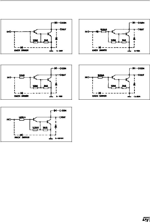
Five versions are available to simplify interfacing to standard logic families : the ULQ2801A is designed for general purpose applications with a current limit resistor ; the ULQ2802A has a 10.5kΩ input resistor and zener for 14-25V PMOS ; the ULQ2803A has a 2.7kΩ input resistor for 5V TTL and CMOS ; the ULQ2804A has a 10.5kΩ input resistor for 6-15V CMOS and the ULQ2805A is designed to sink a minimum of 350mA for standard and Schottky TTL where higher output current is required.
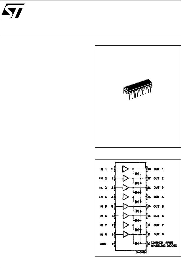
All types are supplied in a 18-lead plastic DIP with a copper lead frame and feature the convenient in- put-opposite-output pinout to simplify board layout.
September 2003
PIN CONNECTION (top view)
1/8 |

ULQ2801A - ULQ2802A - ULQ2803A - ULQ2804A - ULQ2805A
SCHEMATIC DIAGRAM AND ORDER CODES
For ULQ2801A (each driver for PMOS-CMOS) For ULQ2802A (each driver for 14-15 V PMOS)
For ULQ2803A (each driver for 5 V, TTL/CMOS)
For ULQ2804A (each driver for 6-15 V |
CMOS/PMOS |
For ULQ2805A (each driver for high out TTL)
ABSOLUTE MAXIMUM RATINGS
Symbol |
Parameter |
Value |
Unit |
|
|
|
|
Vo |
Output Voltage |
50 |
V |
Vi |
Input Voltage for ULQ2802A, 2803A, 2804A |
30 |
V |
|
for ULQ2805A |
15 |
V |
IC |
Continuous Collector Current |
500 |
mA |
IB |
Continuous Base Current |
25 |
mA |
Ptot |
Power Dissipation (one Darlington pair) |
1.0 |
W |
|
(total package) |
2.25 |
W |
Tamb |
Operating Ambient Temperature Range |
– 40 to 105 |
°C |
Tstg |
Storage Temperature Range |
– 55 to 150 |
°C |
|
|
|
|
THERMAL DATA
Symbol |
Parameter |
|
Value |
Unit |
|
|
|
|
|
Rth j-amb |
Thermal Resistance Junction-ambient |
Max. |
55 |
°C/W |
|
|
|
|
|
2/8 |
|
|
|
|
|
|
|
|
|

ULQ2801A - ULQ2802A - ULQ2803A - ULQ2804A - ULQ2805A
ELECTRICAL CHARACTERISTICS (Tj = –40 to 105oC, unless otherwise specified)
Symbol |
Parameter |
Test Conditions |
Min. |
Typ. |
Max. |
Unit |
Fig. |
|
ICEX |
Output Leakage Current |
VCE = 50V |
|
|
|
50 |
μA |
1a |
|
|
TJ = 105°C, VCE = 50V |
|
|
100 |
μA |
1a |
|
|
|
TJ = 105°C |
|
|
|
500 |
μA |
1b |
|
|
for ULQ2802A VCE = 50V, Vi = 6V |
|
|
||||
|
|
for ULQ2804A VCE = 50V, Vi = 1V |
|
|
500 |
μA |
1b |
|
VCE (sat) |
Collector-emitter |
IC = 100mA, IB = 250μA |
|
0.9 |
1.1 |
V |
2 |
|
|
Saturation Voltage |
IC = 200mA, IB = 350μA |
|
1.1 |
1.3 |
V |
||
|
|
IC = 350mA, IB = 500μA |
|
1.3 |
1.6 |
V |
|
|
Ii(on) |
Input Current |
for ULQ2802A |
Vi = 17V |
|
0.82 |
1.25 |
mA |
|
|
|
for ULQ2803A |
Vi = 3.85V |
|
0.93 |
1.35 |
mA |
|
|
|
for ULQ2804A |
Vi = 5V |
|
0.35 |
0.5 |
mA |
3 |
|
|
for ULQ2805A |
Vi = 12V |
|
1 |
1.45 |
mA |
|
|
|
Vi = 3V |
|
1.5 |
2.4 |
mA |
|
|
Ii(off) |
Input Current |
TJ = 105°C, IC = 500μA |
50 |
65 |
|
μA |
4 |
|
Vi(on) |
Input Voltage |
for ULQ2802A VCE = 2V, Ic = 300mA |
|
|
13 |
V |
|
|
|
|
for ULQ2803A VCE = 2V, Ic = 200mA |
|
|
2.4 |
V |
|
|
|
|
|
VCE = 2V, Ic = 250mA |
|
|
2.7 |
V |
|
|
|
|
VCE = 2V, Ic = 300mA |
|
|
3 |
V |
|
|
|
for ULQ2804A VCE = 2V, Ic = 125mA |
|
|
5 |
V |
5 |
|
|
|
|
VCE = 2V, Ic = 200mA |
|
|
6 |
V |
|
|
|
|
VCE = 2V, Ic = 275mA |
|
|
7 |
V |
|
|
|
|
VCE = 2V, Ic = 350mA |
|
|
8 |
V |
|
|
|
for ULQ2805A VCE = 2V, Ic = 350mA |
|
|
2.4 |
V |
|
|
hFE |
DC Forward Current Gain |
for ULQ2802A VCE = 2V, Ic = 350mA |
1000 |
|
|
– |
2 |
|
Ci |
Input Capacitance |
|
|
|
15 |
25 (*) |
pF |
– |
tPLH |
Turn-on Delay Time |
0.5 Vi to 0.5 Vo |
|
|
0.25 |
1 (*) |
μs |
– |
tPHL |
Turn-off Delay Time |
0.5 Vi to 0.5 Vo |
|
|
0.25 |
1 (*) |
μs |
– |
IR |
Clamp Diode Leakage |
VR = 50V |
|
|
|
50 |
μA |
6 |
|
Current |
TJ = 105°C, VR = 50V |
|
|
100 |
μA |
|
|
VF |
Clamp Diode Forward |
IF = 350mA |
|
|
1.7 |
2 |
V |
7 |
|
Voltage |
|
|
|
|
|
|
|
(*) Guaranteed by design
3/8
 Loading...