


 Loading...
ST PC560B60L7, SPC560B64L7, SPC560B54L5, SPC560B60L5, SPC560B64L5 User Manual
...SPC560B54x SPC560B60x, SPC560B64x
32-bit MCU family built on the Power Architecture® for automotive body electronics applications
Features
■High performance 64 MHz e200z0h CPU
–32-bit Power Architecture® technology CPU
–Up to 60 DMIPs operation
–Variable length encoding (VLE)
■Memory
–Up to 1.5 MB on-chip Code Flash with ECC
–64 KB on-chip Data Flash with ECC
–Up to 96 KB on-chip SRAM with ECC
–8-entry MPU
■Interrupts
–16 priority levels
–Non-maskable interrupt (NMI)
–Up to 51 external interrupts lines including 27 wake-up lines
■16-channel eDMA (linked to PITs, DSPI, ADCs, eMIOS, LINFlex and I2C)
■GPIOs: 77 (LQFP100), 121 (LQFP144) and 149 (LQFP176)
■Timer units
–8-channel 32-bit periodic interrupt timer
–4-channel 32-bit system timer
–System watchdog timer
–Real-time clock timer
■eMIOS, 16-bit counter timed I/O units
–Up to 64 channels with PWM/MC/IC/OC
–Up to 10 counter basis
–ADC diagnostic trigger via CTU
■One 10-bit and one 12-bit ADC with up to 53 channels
–Extendable to 81 channels
–Individual conversion registers
–Cross triggering unit (CTU)
■Dedicated diagnostic module for lighting
–Advanced PWM generation
–Time-triggered diagnostics
–PWM-synchronized ADC measurements
■On-chip CAN/UART bootstrap loader
■Communications interfaces
LQFP100 |
LQFP144 |
LQFP176 |
(14 x 14 x 1.4 mm) |
(20 x 20 x 1.4 mm) |
(24 x 24 x 1.4 mm) |
–Up to 6 FlexCAN (2.0B active) with 64 message buffers each
–Up to 10 LINFlex/UART channels
–Up to 6 buffered DSPI channels
–I2C interface
■Clock generation
–4 to 16 MHz fast external crystal oscillator
–32 kHz slow external crystal oscillator
–16 MHz fast internal RC oscillator
–128 kHz slow internal RC oscillator for lowpower modes
–Software-controlled FMPLL
–Clock monitoring unit
■Low-power capabilities
–Several low-power mode configurations
–Ultra-low-power standby with RTC and communication
–Fast wakeup schemes
■Exhaustive debugging capability
–Nexus 2+ interface on LBGA208 package
–Nexus 1 on all packages
■Voltage supply
–Single 5 V or 3.3 V supply
–On-chip voltage regulator
–External ballast resistor support
■LQFP100, LQFP144, and LQFP176 packages; LBGA208 package for Nexus2+
■Operating temperature range -40 to 125 °C
Table 1. |
Device summary |
|
|
Package |
768 KByte |
1 MByte |
1.5 MByte |
|
Code Flash |
Code Flash |
Code Flash |
|
|
|
|
LQFP176 |
— |
SPC560B60L7 |
SPC560B64L7 |
|
|
|
|
LQFP144 |
SPC560B54L5 |
SPC560B60L5 |
SPC560B64L5 |
|
|
|
|
LQFP100 |
SPC560B54L3 |
SPC560B60L3 |
— |
|
|
|
|
September 2011 |
Doc ID 15131 Rev 6 |
1/134 |
www.st.com

Contents |
SPC560B54/6x |
|
|
Contents
1 |
Introduction . . . . . . . . . . . . . . . . . . . . . . . . . . . . . . . . . . . . . . . . . . . . . . . |
. 8 |
|
|
1.1 |
Document overview . . . . . . . . . . . . . . . . . . . . . . . . . . . . . . . . . . . . . . . . . . |
8 |
|
1.2 |
Description . . . . . . . . . . . . . . . . . . . . . . . . . . . . . . . . . . . . . . . . . . . . . . . . . |
8 |
2 |
Block diagram . . . . . . . . . . . . . . . . . . . . . . . . . . . . . . . . . . . . . . . . . . . . . |
10 |
|
3 |
Package pinouts and signal descriptions . . . . . . . . . . . . . . . . . . . . . . . |
13 |
|
|
3.1 |
Package pinouts . . . . . . . . . . . . . . . . . . . . . . . . . . . . . . . . . . . . . . . . . . . . |
13 |
|
3.2 |
Pad configuration during reset phases . . . . . . . . . . . . . . . . . . . . . . . . . . . |
16 |
|
3.3 |
Pad configuration during standby mode exit . . . . . . . . . . . . . . . . . . . . . . |
17 |
|
3.4 |
Voltage supply pins . . . . . . . . . . . . . . . . . . . . . . . . . . . . . . . . . . . . . . . . . |
17 |
|
3.5 |
Pad types . . . . . . . . . . . . . . . . . . . . . . . . . . . . . . . . . . . . . . . . . . . . . . . . . |
18 |
|
3.6 |
System pins . . . . . . . . . . . . . . . . . . . . . . . . . . . . . . . . . . . . . . . . . . . . . . . |
18 |
|
3.7 |
Functional port pins . . . . . . . . . . . . . . . . . . . . . . . . . . . . . . . . . . . . . . . . . |
20 |
|
3.8 |
Nexus 2+ pins . . . . . . . . . . . . . . . . . . . . . . . . . . . . . . . . . . . . . . . . . . . . . . |
56 |
4 |
Electrical characteristics . . . . . . . . . . . . . . . . . . . . . . . . . . . . . . . . . . . . |
57 |
|
|
4.1 |
Parameter classification . . . . . . . . . . . . . . . . . . . . . . . . . . . . . . . . . . . . . . |
57 |
|
4.2 |
NVUSRO register . . . . . . . . . . . . . . . . . . . . . . . . . . . . . . . . . . . . . . . . . . . |
57 |
4.2.1 NVUSRO[PAD3V5V] field description . . . . . . . . . . . . . . . . . . . . . . . . . . 58 4.2.2 NVUSRO[OSCILLATOR_MARGIN] field description . . . . . . . . . . . . . . . 58 4.2.3 NVUSRO[WATCHDOG_EN] field description . . . . . . . . . . . . . . . . . . . . 58
4.3 Absolute maximum ratings . . . . . . . . . . . . . . . . . . . . . . . . . . . . . . . . . . . . 59 4.4 Recommended operating conditions . . . . . . . . . . . . . . . . . . . . . . . . . . . . 60 4.5 Thermal characteristics . . . . . . . . . . . . . . . . . . . . . . . . . . . . . . . . . . . . . . 61
4.5.1 External ballast resistor recommendations . . . . . . . . . . . . . . . . . . . . . . 61 4.5.2 Package thermal characteristics . . . . . . . . . . . . . . . . . . . . . . . . . . . . . . 62 4.5.3 Power considerations . . . . . . . . . . . . . . . . . . . . . . . . . . . . . . . . . . . . . . . 63
4.6 |
I/O pad electrical characteristics . . . . . . . . . . . . . . . . . . . . . . . . . . . . . . . |
64 |
|
|
4.6.1 |
I/O pad types . . . . . . . . . . . . . . . . . . . . . . . . . . . . . . . . . . . . . . . . . . . . . |
64 |
|
4.6.2 |
I/O input DC characteristics . . . . . . . . . . . . . . . . . . . . . . . . . . . . . . . . . . |
64 |
|
4.6.3 |
I/O output DC characteristics . . . . . . . . . . . . . . . . . . . . . . . . . . . . . . . . . |
65 |
|
4.6.4 |
Output pin transition times . . . . . . . . . . . . . . . . . . . . . . . . . . . . . . . . . . . |
68 |
2/134 |
Doc ID 15131 Rev 6 |

SPC560B54/6x |
Contents |
|
|
4.6.5 I/O pad current specification . . . . . . . . . . . . . . . . . . . . . . . . . . . . . . . . . 69
4.7 RESET electrical characteristics . . . . . . . . . . . . . . . . . . . . . . . . . . . . . . . 78 4.8 Power management electrical characteristics . . . . . . . . . . . . . . . . . . . . . 80
4.8.1 |
Voltage regulator electrical characteristics . . . . . . . . . . . . . . . . . . . . . . |
80 |
4.8.2 |
Low voltage detector electrical characteristics . . . . . . . . . . . . . . . . . . . . |
83 |
4.9 Power consumption . . . . . . . . . . . . . . . . . . . . . . . . . . . . . . . . . . . . . . . . . 84 4.10 Flash memory electrical characteristics . . . . . . . . . . . . . . . . . . . . . . . . . . 86
4.10.1 Program/erase characteristics . . . . . . . . . . . . . . . . . . . . . . . . . . . . . . . . 86 4.10.2 Flash power supply DC characteristics . . . . . . . . . . . . . . . . . . . . . . . . . 87 4.10.3 Start-up/Switch-off timings . . . . . . . . . . . . . . . . . . . . . . . . . . . . . . . . . . . 88
4.11 Electromagnetic compatibility (EMC) characteristics . . . . . . . . . . . . . . . . 88
4.11.1 Designing hardened software to avoid noise problems . . . . . . . . . . . . . |
88 |
|
4.11.2 |
Electromagnetic interference (EMI) . . . . . . . . . . . . . . . . . . . . . . . . . . . . |
89 |
4.11.3 |
Absolute maximum ratings (electrical sensitivity) . . . . . . . . . . . . . . . . . |
89 |
4.12Fast external crystal oscillator (4 to 16 MHz) electrical characteristics . . 90
4.13 |
Slow external crystal oscillator (32 kHz) electrical characteristics . . . . . . |
93 |
|
4.14 |
FMPLL electrical characteristics . . . . . . . . . . . . . . . . . . . . . . . . . . . . . . . |
95 |
|
4.15 |
Fast internal RC oscillator (16 MHz) electrical characteristics . . . . . . . . . |
96 |
|
4.16 |
Slow internal RC oscillator (128 kHz) electrical characteristics . . . . . . . . |
97 |
|
4.17 |
ADC electrical characteristics . . . . . . . . . . . . . . . . . . . . . . . . . . . . . . . . . |
98 |
|
|
4.17.1 |
Introduction . . . . . . . . . . . . . . . . . . . . . . . . . . . . . . . . . . . . . . . . . . . . . |
. 98 |
|
4.17.2 Input impedance and ADC accuracy . . . . . . . . . . . . . . . . . . . . . . . . . . |
. 99 |
|
|
4.17.3 |
ADC electrical characteristics . . . . . . . . . . . . . . . . . . . . . . . . . . . . . . . |
104 |
4.18 On-chip peripherals . . . . . . . . . . . . . . . . . . . . . . . . . . . . . . . . . . . . . . . . 109
4.18.1 Current consumption . . . . . . . . . . . . . . . . . . . . . . . . . . . . . . . . . . . . . . 109 4.18.2 DSPI characteristics . . . . . . . . . . . . . . . . . . . . . . . . . . . . . . . . . . . . . . 111 4.18.3 Nexus characteristics . . . . . . . . . . . . . . . . . . . . . . . . . . . . . . . . . . . . . . 117 4.18.4 JTAG characteristics . . . . . . . . . . . . . . . . . . . . . . . . . . . . . . . . . . . . . . 118
5 |
Package characteristics . . . . . . . . . . . . . . . . . . . . . . . . . . . . . . . . . . . . |
120 |
|
|
5.1 |
ECOPACK® . . . . . . . . . . . . . . . . . . . . . . . . . . . . . . . . . . . . . . . . . . . . . . |
120 |
|
5.2 |
Package mechanical data . . . . . . . . . . . . . . . . . . . . . . . . . . . . . . . . . . . |
120 |
5.2.1 LQFP176 . . . . . . . . . . . . . . . . . . . . . . . . . . . . . . . . . . . . . . . . . . . . . . . 120 5.2.2 LQFP144 . . . . . . . . . . . . . . . . . . . . . . . . . . . . . . . . . . . . . . . . . . . . . . . 122 5.2.3 LQFP100 . . . . . . . . . . . . . . . . . . . . . . . . . . . . . . . . . . . . . . . . . . . . . . . 124
Doc ID 15131 Rev 6 |
3/134 |

Contents |
|
|
SPC560B54/6x |
|
|
|
|
|
5.2.4 |
LBGA208 . . . . . . . . . . . . . . . . . . . . . . . . . . . . . . . . . . . . . . |
. . . . . . . . . 126 |
6 |
Ordering information . . . . . . . . . . . . . . . . . . . . . . . . . . . . . . . |
. . . . . . . 128 |
|
Appendix A Abbreviations . . . . . . . . . . . . . . . . . . . . . . . . . . . . . . . . . . . |
. . . . . . . 129 |
||
Revision history . . . . . |
. . . . . . . . . . . . . . . . . . . . . . . . . . . . . . . . . . . . . . . |
. . . . . . . 130 |
|
4/134 |
Doc ID 15131 Rev 6 |

SPC560B54/6x |
List of tables |
|
|
List of tables
Table 1. Device summary . . . . . . . . . . . . . . . . . . . . . . . . . . . . . . . . . . . . . . . . . . . . . . . . . . . . . . . . . . 1 Table 2. SPC560B54/6 family comparison . . . . . . . . . . . . . . . . . . . . . . . . . . . . . . . . . . . . . . . . . . . . . 8 Table 3. SPC560B54/6 series block summary . . . . . . . . . . . . . . . . . . . . . . . . . . . . . . . . . . . . . . . . . 11 Table 4. Voltage supply pin descriptions . . . . . . . . . . . . . . . . . . . . . . . . . . . . . . . . . . . . . . . . . . . . . 17 Table 5. System pin descriptions . . . . . . . . . . . . . . . . . . . . . . . . . . . . . . . . . . . . . . . . . . . . . . . . . . . 19 Table 6. Functional port pin descriptions . . . . . . . . . . . . . . . . . . . . . . . . . . . . . . . . . . . . . . . . . . . . . 20 Table 7. Nexus 2+ pin descriptions. . . . . . . . . . . . . . . . . . . . . . . . . . . . . . . . . . . . . . . . . . . . . . . . . . 56 Table 8. Parameter classifications . . . . . . . . . . . . . . . . . . . . . . . . . . . . . . . . . . . . . . . . . . . . . . . . . . 57 Table 9. PAD3V5V field description . . . . . . . . . . . . . . . . . . . . . . . . . . . . . . . . . . . . . . . . . . . . . . . . . 58 Table 10. OSCILLATOR_MARGIN field description. . . . . . . . . . . . . . . . . . . . . . . . . . . . . . . . . . . . . . 58 Table 11. WATCHDOG_EN field description . . . . . . . . . . . . . . . . . . . . . . . . . . . . . . . . . . . . . . . . . . . 58 Table 12. Absolute maximum ratings . . . . . . . . . . . . . . . . . . . . . . . . . . . . . . . . . . . . . . . . . . . . . . . . . 59 Table 13. Recommended operating conditions (3.3 V) . . . . . . . . . . . . . . . . . . . . . . . . . . . . . . . . . . . 60 Table 14. Recommended operating conditions (5.0 V) . . . . . . . . . . . . . . . . . . . . . . . . . . . . . . . . . . . 60 Table 15. LQFP thermal characteristics . . . . . . . . . . . . . . . . . . . . . . . . . . . . . . . . . . . . . . . . . . . . . . . 62 Table 16. I/O input DC electrical characteristics. . . . . . . . . . . . . . . . . . . . . . . . . . . . . . . . . . . . . . . . . 65 Table 17. I/O pull-up/pull-down DC electrical characteristics . . . . . . . . . . . . . . . . . . . . . . . . . . . . . . . 65 Table 18. SLOW configuration output buffer electrical characteristics . . . . . . . . . . . . . . . . . . . . . . . . 66 Table 19. MEDIUM configuration output buffer electrical characteristics . . . . . . . . . . . . . . . . . . . . . . 67 Table 20. FAST configuration output buffer electrical characteristics. . . . . . . . . . . . . . . . . . . . . . . . . 67 Table 21. Output pin transition times . . . . . . . . . . . . . . . . . . . . . . . . . . . . . . . . . . . . . . . . . . . . . . . . . 68 Table 22. I/O supply segments . . . . . . . . . . . . . . . . . . . . . . . . . . . . . . . . . . . . . . . . . . . . . . . . . . . . . . 69 Table 23. I/O consumption . . . . . . . . . . . . . . . . . . . . . . . . . . . . . . . . . . . . . . . . . . . . . . . . . . . . . . . . . 69 Table 24. I/O weight . . . . . . . . . . . . . . . . . . . . . . . . . . . . . . . . . . . . . . . . . . . . . . . . . . . . . . . . . . . . . . 71 Table 25. Reset electrical characteristics . . . . . . . . . . . . . . . . . . . . . . . . . . . . . . . . . . . . . . . . . . . . . . 79 Table 26. Voltage regulator electrical characteristics . . . . . . . . . . . . . . . . . . . . . . . . . . . . . . . . . . . . . 81 Table 27. Low voltage detector electrical characteristics . . . . . . . . . . . . . . . . . . . . . . . . . . . . . . . . . . 84 Table 28. Power consumption on VDD_BV and VDD_HV . . . . . . . . . . . . . . . . . . . . . . . . . . . . . . . . . 84 Table 29. Program and erase specifications . . . . . . . . . . . . . . . . . . . . . . . . . . . . . . . . . . . . . . . . . . . 86 Table 30. Flash module life. . . . . . . . . . . . . . . . . . . . . . . . . . . . . . . . . . . . . . . . . . . . . . . . . . . . . . . . . 86 Table 31. Flash read access timing . . . . . . . . . . . . . . . . . . . . . . . . . . . . . . . . . . . . . . . . . . . . . . . . . . 87 Table 32. Flash power supply DC electrical characteristics . . . . . . . . . . . . . . . . . . . . . . . . . . . . . . . . 87 Table 33. Start-up time/Switch-off time. . . . . . . . . . . . . . . . . . . . . . . . . . . . . . . . . . . . . . . . . . . . . . . . 88 Table 34. EMI radiated emission measurement . . . . . . . . . . . . . . . . . . . . . . . . . . . . . . . . . . . . . . . . . 89 Table 35. ESD absolute maximum ratings . . . . . . . . . . . . . . . . . . . . . . . . . . . . . . . . . . . . . . . . . . . . . 90 Table 36. Latch-up results . . . . . . . . . . . . . . . . . . . . . . . . . . . . . . . . . . . . . . . . . . . . . . . . . . . . . . . . . 90 Table 37. Crystal description . . . . . . . . . . . . . . . . . . . . . . . . . . . . . . . . . . . . . . . . . . . . . . . . . . . . . . . 91 Table 38. Fast external crystal oscillator (4 to 16 MHz) electrical characteristics. . . . . . . . . . . . . . . . 92 Table 39. Crystal motional characteristics . . . . . . . . . . . . . . . . . . . . . . . . . . . . . . . . . . . . . . . . . . . . . 94 Table 40. Slow external crystal oscillator (32 kHz) electrical characteristics . . . . . . . . . . . . . . . . . . . 95 Table 41. FMPLL electrical characteristics . . . . . . . . . . . . . . . . . . . . . . . . . . . . . . . . . . . . . . . . . . . . . 95 Table 42. Fast internal RC oscillator (16 MHz) electrical characteristics . . . . . . . . . . . . . . . . . . . . . . 96 Table 43. Slow internal RC oscillator (128 kHz) electrical characteristics . . . . . . . . . . . . . . . . . . . . . 97 Table 44. ADC input leakage current . . . . . . . . . . . . . . . . . . . . . . . . . . . . . . . . . . . . . . . . . . . . . . . . 104 Table 45. ADC_0 conversion characteristics (10-bit ADC_0). . . . . . . . . . . . . . . . . . . . . . . . . . . . . . 104 Table 46. ADC_1 conversion characteristics (12-bit ADC_1). . . . . . . . . . . . . . . . . . . . . . . . . . . . . . 106 Table 47. On-chip peripherals current consumption. . . . . . . . . . . . . . . . . . . . . . . . . . . . . . . . . . . . . 109 Table 48. DSPI characteristics . . . . . . . . . . . . . . . . . . . . . . . . . . . . . . . . . . . . . . . . . . . . . . . . . . . . . 111
Doc ID 15131 Rev 6 |
5/134 |

List of tables |
SPC560B54/6x |
|
|
Table 49. Nexus characteristics . . . . . . . . . . . . . . . . . . . . . . . . . . . . . . . . . . . . . . . . . . . . . . . . . . . . 117 Table 50. JTAG characteristics. . . . . . . . . . . . . . . . . . . . . . . . . . . . . . . . . . . . . . . . . . . . . . . . . . . . . 118 Table 51. LQFP176 mechanical data . . . . . . . . . . . . . . . . . . . . . . . . . . . . . . . . . . . . . . . . . . . . . . . . 121 Table 52. LQFP144 mechanical data . . . . . . . . . . . . . . . . . . . . . . . . . . . . . . . . . . . . . . . . . . . . . . . . 123 Table 53. LQFP100 mechanical data . . . . . . . . . . . . . . . . . . . . . . . . . . . . . . . . . . . . . . . . . . . . . . . . 125 Table 54. LBGA208 mechanical data . . . . . . . . . . . . . . . . . . . . . . . . . . . . . . . . . . . . . . . . . . . . . . . . 127 Table 55. Abbreviations . . . . . . . . . . . . . . . . . . . . . . . . . . . . . . . . . . . . . . . . . . . . . . . . . . . . . . . . . . 129 Table 56. Revision history . . . . . . . . . . . . . . . . . . . . . . . . . . . . . . . . . . . . . . . . . . . . . . . . . . . . . . . . 130
6/134 |
Doc ID 15131 Rev 6 |

SPC560B54/6x |
List of figures |
|
|
List of figures
Figure 1. SPC560B54/6 block diagram . . . . . . . . . . . . . . . . . . . . . . . . . . . . . . . . . . . . . . . . . . . . . . . 10 Figure 2. LQFP176 pin configuration . . . . . . . . . . . . . . . . . . . . . . . . . . . . . . . . . . . . . . . . . . . . . . . . . 13 Figure 3. LQFP144 pin configuration . . . . . . . . . . . . . . . . . . . . . . . . . . . . . . . . . . . . . . . . . . . . . . . . . 14 Figure 4. LQFP100 pin configuration . . . . . . . . . . . . . . . . . . . . . . . . . . . . . . . . . . . . . . . . . . . . . . . . . 15 Figure 5. LBGA208 configuration. . . . . . . . . . . . . . . . . . . . . . . . . . . . . . . . . . . . . . . . . . . . . . . . . . . . 16 Figure 6. I/O input DC electrical characteristics definition . . . . . . . . . . . . . . . . . . . . . . . . . . . . . . . . . 64 Figure 7. Start-up reset requirements . . . . . . . . . . . . . . . . . . . . . . . . . . . . . . . . . . . . . . . . . . . . . . . . 78 Figure 8. Noise filtering on reset signal . . . . . . . . . . . . . . . . . . . . . . . . . . . . . . . . . . . . . . . . . . . . . . . 78 Figure 9. Voltage regulator capacitance connection . . . . . . . . . . . . . . . . . . . . . . . . . . . . . . . . . . . . . 81 Figure 10. Low voltage detector vs reset . . . . . . . . . . . . . . . . . . . . . . . . . . . . . . . . . . . . . . . . . . . . . . . 83 Figure 11. Crystal oscillator and resonator connection scheme . . . . . . . . . . . . . . . . . . . . . . . . . . . . . 91 Figure 12. Fast external crystal oscillator (4 to 16 MHz) timing diagram . . . . . . . . . . . . . . . . . . . . . . . 92 Figure 13. Crystal oscillator and resonator connection scheme . . . . . . . . . . . . . . . . . . . . . . . . . . . . . 93 Figure 14. lEquivalent circuit of a quartz crystal . . . . . . . . . . . . . . . . . . . . . . . . . . . . . . . . . . . . . . . . . 94 Figure 15. Slow external crystal oscillator (32 kHz) timing diagram. . . . . . . . . . . . . . . . . . . . . . . . . . . 95 Figure 16. ADC_0 characteristic and error definitions . . . . . . . . . . . . . . . . . . . . . . . . . . . . . . . . . . . . . 99 Figure 17. Input equivalent circuit (precise channels) . . . . . . . . . . . . . . . . . . . . . . . . . . . . . . . . . . . . 100 Figure 18. Input equivalent circuit (extended channels) . . . . . . . . . . . . . . . . . . . . . . . . . . . . . . . . . . 101 Figure 19. Transient behavior during sampling phase. . . . . . . . . . . . . . . . . . . . . . . . . . . . . . . . . . . . 101 Figure 20. Spectral representation of input signal . . . . . . . . . . . . . . . . . . . . . . . . . . . . . . . . . . . . . . . 103 Figure 21. ADC_1 characteristic and error definitions . . . . . . . . . . . . . . . . . . . . . . . . . . . . . . . . . . . . 106 Figure 22. DSPI classic SPI timing — master, CPHA = 0 . . . . . . . . . . . . . . . . . . . . . . . . . . . . . . . . . 113 Figure 23. DSPI classic SPI timing — master, CPHA = 1 . . . . . . . . . . . . . . . . . . . . . . . . . . . . . . . . . 113 Figure 24. DSPI classic SPI timing — slave, CPHA = 0 . . . . . . . . . . . . . . . . . . . . . . . . . . . . . . . . . . 114 Figure 25. DSPI classic SPI timing — slave, CPHA = 1 . . . . . . . . . . . . . . . . . . . . . . . . . . . . . . . . . . 114 Figure 26. DSPI modified transfer format timing — master, CPHA = 0 . . . . . . . . . . . . . . . . . . . . . . . 115 Figure 27. DSPI modified transfer format timing — master, CPHA = 1 . . . . . . . . . . . . . . . . . . . . . . . 115 Figure 28. DSPI modified transfer format timing — slave, CPHA = 0 . . . . . . . . . . . . . . . . . . . . . . . . 116 Figure 29. DSPI modified transfer format timing — slave, CPHA = 1 . . . . . . . . . . . . . . . . . . . . . . . . 116 Figure 30. DSPI PCS strobe (PCSS) timing . . . . . . . . . . . . . . . . . . . . . . . . . . . . . . . . . . . . . . . . . . . 117 Figure 31. Nexus TDI, TMS, TDO timing . . . . . . . . . . . . . . . . . . . . . . . . . . . . . . . . . . . . . . . . . . . . . . 118 Figure 32. Timing diagram — JTAG boundary scan . . . . . . . . . . . . . . . . . . . . . . . . . . . . . . . . . . . . . 119 Figure 33. LQFP176 package mechanical drawing . . . . . . . . . . . . . . . . . . . . . . . . . . . . . . . . . . . . . . 120 Figure 34. LQFP144 package mechanical drawing . . . . . . . . . . . . . . . . . . . . . . . . . . . . . . . . . . . . . . 122 Figure 35. LQFP100 package mechanical drawing . . . . . . . . . . . . . . . . . . . . . . . . . . . . . . . . . . . . . . 124 Figure 36. LBGA208 package mechanical drawing. . . . . . . . . . . . . . . . . . . . . . . . . . . . . . . . . . . . . . 126 Figure 37. Commercial product code structure . . . . . . . . . . . . . . . . . . . . . . . . . . . . . . . . . . . . . . . . . 128
Doc ID 15131 Rev 6 |
7/134 |

Introduction |
SPC560B54/6x |
|
|
1 Introduction
1.1Document overview
This document describes the features of the family and options available within the family members, and highlights important electrical and physical characteristics of the device.
1.2Description
This family of 32-bit system-on-chip (SoC) microcontrollers is the latest achievement in integrated automotive application controllers. It belongs to an expanding family of automotive-focused products designed to address the next wave of body electronics applications within the vehicle.
The advanced and cost-efficient e200z0h host processor core of this automotive controller family complies with the Power Architecture technology and only implements the VLE (variable-length encoding) APU (Auxiliary Processor Unit), providing improved code density. It operates at speeds of up to 64 MHz and offers high performance processing optimized for low power consumption. It capitalizes on the available development infrastructure of current Power Architecture devices and is supported with software drivers, operating systems and configuration code to assist with users implementations.
Table 2. |
SPC560B54/6 family comparison(1) |
|
|
|
|
|
|
|
|
|||
Feature |
SPC560B54 |
|
SPC560B60 |
|
SPC560B64 |
|
||||||
|
|
|
|
|
|
|
|
|
|
|
|
|
CPU |
|
|
|
|
|
e200z0h |
|
|
|
|
||
|
|
|
|
|
|
|
|
|
|
|||
Execution speed(2) |
|
|
|
|
Up to 64 MHz |
|
|
|
|
|||
Code flash memory |
768 KB |
|
|
1 MB |
|
|
|
1.5 MB |
|
|||
|
|
|
|
|
|
|
|
|
|
|||
Data flash memory |
|
|
|
|
64 (4 × 16) KB |
|
|
|
|
|||
SRAM |
|
64 KB |
|
|
80 KB |
|
|
|
96 KB |
|
||
|
|
|
|
|
|
|
|
|
|
|
|
|
MPU |
|
|
|
|
|
8-entry |
|
|
|
|
||
|
|
|
|
|
|
|
|
|
|
|
|
|
eDMA |
|
|
|
|
|
|
16 ch |
|
|
|
|
|
|
|
|
|
|
|
|
|
|
|
|
|
|
10-bit ADC |
|
|
|
|
|
|
Yes |
|
|
|
|
|
|
|
|
|
|
|
|
|
|
|
|
|
|
|
dedicated(3) |
7 ch |
15 ch |
7 ch |
|
15 ch |
|
29 ch |
15 ch |
29 ch |
|
29 ch |
shared with 12-bit ADC |
|
|
|
|
|
19 ch |
|
|
|
|
||
|
|
|
|
|
|
|
|
|
|
|
|
|
12-bit ADC |
|
|
|
|
|
|
Yes |
|
|
|
|
|
|
|
|
|
|
|
|
|
|
|
|
|
|
|
dedicated(4) |
|
|
|
|
|
5 ch |
|
|
|
|
|
shared with 10-bit ADC |
|
|
|
|
|
19 ch |
|
|
|
|
||
|
|
|
|
|
|
|
|
|
|
|
|
|
Total timer I/O(5) eMIOS |
37 ch, |
64 ch, |
37 ch, |
|
64 ch, |
|
64 ch, |
64 ch, |
64 ch, |
|
64 ch, |
|
16-bit |
16-bit |
16-bit |
|
16-bit |
|
16-bit |
16-bit |
16-bit |
|
16-bit |
||
|
|
|
|
|
||||||||
|
|
|
|
|
|
|
|
|
|
|
|
|
Counter / OPWM / |
|
|
|
|
|
10 ch |
|
|
|
|
||
|
ICOC(6) |
|
|
|
|
|
|
|
|
|
||
|
|
|
|
|
|
|
|
|
|
|
|
|
O(I)PWM / OPWFMB / |
|
|
|
|
|
7 ch |
|
|
|
|
||
OPWMCB / ICOC(7) |
|
|
|
|
|
|
|
|
|
|||
|
|
|
|
|
|
|
|
|
|
|
||
8/134 |
Doc ID 15131 Rev 6 |

SPC560B54/6x |
|
|
|
|
|
|
|
|
Introduction |
||
|
|
|
|
|
|
|
|
|
|
|
|
Table 2. |
SPC560B54/6 family comparison(1) (continued) |
|
|
|
|
||||||
Feature |
SPC560B54 |
|
SPC560B60 |
|
|
SPC560B64 |
|||||
|
|
|
|
|
|
|
|
|
|
|
|
O(I)PWM / ICOC(8) |
7 ch |
14 ch |
7 ch |
|
14 ch |
|
14 ch |
14 ch |
14 ch |
14 ch |
|
OPWM / ICOC(9) |
13 ch |
33 ch |
13 ch |
|
33 ch |
|
33 ch |
33 ch |
33 ch |
33 ch |
|
SCI (LINFlex) |
|
4 |
8 |
4 |
|
8 |
|
10 |
8 |
10 |
10 |
|
|
|
|
|
|
|
|
|
|
|
|
SPI (DSPI) |
|
3 |
5 |
3 |
|
5 |
|
6 |
5 |
6 |
6 |
|
|
|
|
|
|
|
|
|
|
|
|
CAN (FlexCAN) |
|
|
|
6 |
|
|
|
|
|||
|
|
|
|
|
|
|
|
|
|
||
I2C |
|
|
|
|
1 |
|
|
|
|
||
32 KHz oscillator |
|
|
|
|
Yes |
|
|
|
|
||
|
|
|
|
|
|
|
|
|
|
|
|
GPIO(10) |
|
77 |
121 |
77 |
|
121 |
|
149 |
121 |
149 |
149 |
Debug |
|
|
|
|
|
JTAG |
|
|
|
N2+ |
|
|
|
|
|
|
|
|
|
|
|
|
|
Package |
|
LQFP100 |
LQFP144 |
LQFP100 |
LQFP144 |
LQFP176 |
LQFP144 |
LQFP176 |
LBGA208 |
||
|
(11) |
||||||||||
|
|
|
|
|
|
|
|
|
|
|
|
1.Feature set dependent on selected peripheral multiplexing; table shows example
2.Based on 125 °C ambient operating temperature
3.Not shared with 12-bit ADC, but possibly shared with other alternate functions
4.Not shared with 10-bit ADC, but possibly shared with other alternate functions
5.See the eMIOS section of the chip reference manual for information on the channel configuration and functions.
6.Each channel supports a range of modes including Modulus counters, PWM generation, Input Capture, Output Compare.
7.Each channel supports a range of modes including PWM generation with dead time, Input Capture, Output Compare.
8.Each channel supports a range of modes including PWM generation, Input Capture, Output Compare, Period and Pulse width measurement.
9.Each channel supports a range of modes including PWM generation, Input Capture, and Output Compare.
10.Maximum I/O count based on multiplexing with peripherals
11.LBGA208 available only as development package for Nexus2+
Doc ID 15131 Rev 6 |
9/134 |

Block diagram |
SPC560B54/6x |
|
|
2 Block diagram
Figure 1 shows a top-level block diagram of the SPC560B54/6.
Figure 1. SPC560B54/6 block diagram
JTAG Port
Nexus Port
NMI
Clocks
|
|
JTAG |
|
|
|
|
eDMA |
SRAM |
Code Flash |
Data Flash |
|
|
|
|
|
|
|
96 KB |
1.5 MB |
64 KB |
|||
|
|
|
|
|
|
|
|
|
|||
|
|
|
|
|
|
(Master) |
|
|
|
|
|
|
|
|
|
|
Instructions |
Switch |
|
SRAM |
|
|
|
Nexus |
|
|
e200z0h |
(Master) |
|
Flash |
|||||
|
|
|
|
Controller |
Controller |
||||||
|
|
|
|
|
|
|
Crossbar |
MPU |
|||
|
|
SIUL |
|
|
Data |
|
|
|
|
||
|
|
NMI |
|
Nexus 2+ |
|
|
|
|
(Slave) |
|
|
|
|
|
|
(Master) |
|
|
|
(Slave) |
|||
|
|
|
|
|
|
|
|
||||
Voltage |
|
|
|
|
|
|
3 |
|
|
|
|
|
|
|
|
|
|
2 x |
|
|
|
|
|
Regulator |
|
|
|
|
|
|
|
|
|
Interrupt |
|
|
|
Interrupt requests |
|
|
|
64-bit |
|
|
|
request with |
|
|
|
from peripheral |
|
|
|
|
(Slave) |
|
wakeup |
||
|
|
blocks |
|
|
MPU |
|
|
|
|
|
functionality |
|
|
|
|
INTC |
|
|
|
|
WKPU |
|
|
|
|
|
|
Registers |
|
|
|
|
|
||
|
|
CMU |
|
|
|
|
|
|
|
|
|
FMPLL |
|
|
|
|
|
|
|
|
|
|
|
RTC |
STM |
SWT |
ECSM |
PIT |
MC_RGM |
MC_CGM |
MC_ME |
MC_PCU |
BAM |
SSCM |
|
|
|
|
|
|
|||||||
|
|
|
|
|
Peripheral Bridge |
|
|
|
|
|
|
|
|
|
|
|
|
|
|
|
|
|
|
|
|
|
|
|
|
|
|
|
|
|
|
|
|
|
|
|
|
|
|
|
|
|
|
|
|
|
|
|
|
|
|
|
|
|
|
|
|
|
|
|
|
|
|
|
|
|
|
|
|
|
|
|
|
|
|
|
|
|
|
|
|
|
|
|
|
|
|
|
|
|
|
|
|
|
|
|
|
|
|
|
|
|
|
|
|
|
|
|
|
|
|
|
|
|
|
SIUL |
|
19 ch 10-bit/12-bit |
|
29 ch 10-bit |
|
|
|
CTU |
|
|
|
64 ch |
|
10 x |
|
6 x |
|
|
I2C |
|
|
6 x |
||||||||||||||||||||||
Interrupt |
|
Reset Control |
|
ADC |
|
ADC |
|
|
|
|
|
|
|
|
|
eMIOS |
|
LINFlex |
|
DSPI |
|
|
|
|
|
FlexCAN |
||||||||||||||||||||||||
|
|
|
|
|
|
|
|
|
|
|
|
|
|
|
|
|
|
|
|
|
|
|
|
|
|
|
|
|
|
|
|
|
|
|
|
|
|
|
|
|
|
|
|
|
|
|
|
|||
Request |
|
|
External |
|
|
|
|
|
|
|
|
|
|
|
|
|
|
|
|
|
|
|
|
|
|
|
|
|
|
|
|
|
|
|
|
|
|
|
|
|
|
|
||||||||
|
|
|
|
|
Interrupt |
|
|
|
|
|
|
|
|
|
|
|
|
|
|
|
|
|
|
|
|
|
|
|
|
|
|
|
|
|
|
|
|
|
|
|
|
|
|
|
||||||
|
|
|
|
|
|
|
|
|
|
|
|
|
|
|
|
|
|
|
|
|
|
|
|
|
|
|
|
|
|
|
|
|
|
|
|
|
|
|
|
|
|
|
||||||||
|
|
|
|
|
Request |
|
|
|
|
|
|
|
|
|
|
|
|
|
|
|
|
|
|
|
|
|
|
|
|
|
|
|
|
|
|
|
|
|
|
|
|
|
|
|
||||||
|
|
|
|
|
|
|
|
|
|
|
5 ch 12-bit |
|
|
|
|
|
|
|
|
|
|
|
|
|
|
|
|
|
|
|
|
|
|
|
|
|
|
|
|
|
||||||||||
|
|
|
|
|
|
|
|
|
|
|
|
|
|
|
|
|
|
|
|
|
|
|
|
|
|
|
|
|
|
|
|
|
|
|
|
|
|
|
|
|
|
|
|
|
|
|
|
|||
|
|
|
|
|
|
IMUX |
|
|
|
|
|
|
|
|
ADC |
|
|
|
|
|
|
|
|
|
|
|
|
|
|
|
|
|
|
|
|
|
|
|
|
|
|
|
|
|
||||||
|
|
|
|
|
|
|
|
|
|
|
|
|
|
|
|
|
|
|
|
|
|
|
|
|
|
|
|
|
|
|
|
|
|
|
|
|
|
|
|
|
|
|
|
|
|
|
|
|
|
|
|
|
|
|
|
GPIO & |
|
|
|
|
|
|
|
|
|
|
|
|
|
|
|
|
|
|
|
|
|
|
|
|
|
|
|
|
|
|
|
|
|
|
|
|
|
|
|
||||||
|
|
|
|
Pad Control |
|
|
|
|
|
|
|
|
|
|
|
|
|
|
|
|
|
|
|
|
|
|
|
|
|
|
|
|
|
|
|
|
|
|
|
|
|
|
|
|||||||
|
|
|
|
|
|
|
|
|
|
|
|
|
|
|
|
|
|
|
|
|
|
|
|
|
|
|
|
|
|
|
|
|
|
|
|
|
|
|
|
|
|
|
|
|
|
|
|
|
|
|
|
|
|
|
|
|
|
|
|
|
|
|
|
|
|
|
|
|
|
|
|
|
|
|
|
|
|
|
|
|
|
|
|
|
|
|
|
|
|
|
|
|
|
|
|
|
|
|
|
|
|
|
|
|
|
|
|
|
|
|
|
|
|
|
|
|
|
|
|
|
|
|
|
|
|
|
|
|
|
|
|
|
|
|
|
|
|
|
|
|
|
|
|
|
|
|
|
|
|
|
|
|
|
|
|
|
|
|
|
|
|
|
|
|
|
|
|
|
|
|
|
|
|
|
|
|
|
|
|
|
|
|
|
|
|
|
|
|
|
|
|
|
|
|
|
|
|
|
|
|
|
|
|
|
|
|
|
|
|
|
|
|
|
|
|
|
|
|
|
|
|
|
|
|
|
|
|
|
|
|
|
|
|
|
|
|
|
|
|
|
|
|
|
|
|
|
|
|
|
|
|
|
|
|
|
|
|
|
|
|
|
|
|
|
|
|
|
|
|
|
|
|
|
|
|
|
|
|
|
|
|
|
|
|
|
|
|
|
|
|
|
|
|
|
|
|
|
|
|
|
|
|
|
|
|
|
|
|
|
|
|
|
|
|
|
|
|
|
|
|
|
|
|
|
|
|
|
|
|
|
|
|
|
|
|
|
|
|
|
|
|
|
|
|
|
|
|
|
|
|
|
|
|
|
|
|
|
|
|
|
|
|
|
|
|
|
|
|
|
|
|
|
|
|
|
|
|
|
|
|
|
|
|
|
|
|
|
|
|
|
|
|
|
|
|
|
|
|
|
|
|
|
|
|
|
|
|
I/O |
. . . |
. . . |
. . . |
. . . |
. . . |
|
|
|
|
|
Legend:
ADC |
Analog-to-Digital Converter |
MC_CGM |
Clock Generation Module |
BAM |
Boot Assist Module |
MC_ME |
Mode Entry Module |
CMU |
Clock Monitor Unit |
MC_PCU |
Power Control Unit |
CTU |
Cross Triggering Unit |
MC_RGM |
Reset Generation Module |
DSPI |
Deserial Serial Peripheral Interface |
MPU |
Memory Protection Unit |
ECSM |
Error Correction Status Module |
NMI |
Non-Maskable Interrupt |
eDMA |
Enhanced Direct Memory Access |
PIT |
Periodic Interrupt Timer |
eMIOS |
Enhanced Modular Input Output System |
RTC |
Real-Time Clock |
Flash |
Flash memory |
SIUL |
System Integration Unit Lite |
FlexCAN |
Controller Area Network |
SRAM |
Static Random-Access Memory |
FMPLL |
Frequency-Modulated Phase-Locked Loop |
SSCM |
System Status Configuration Module |
GPIO |
General-purpose input/output |
STM |
System Timer Module |
I2C |
Inter-Integrated Circuit bus |
SWT |
Software Watchdog Timer |
IMUX |
Internal Multiplexer |
VREG |
Voltage regulator |
INTC |
Interrupt Controller |
WKPU |
Wakeup Unit |
JTAG |
JTAG controller |
XBAR |
Crossbar switch |
LINFlex |
Serial Communication Interface (LIN support) |
|
|
10/134 |
Doc ID 15131 Rev 6 |
SPC560B54/6x |
Block diagram |
||
|
|
|
|
|
Table 3 summarizes the functions of the blocks present on the SPC560B54/6. |
||
Table 3. |
SPC560B54/6 series block summary |
||
|
|
|
|
|
Block |
Function |
|
|
|
||
Analog-to-digital converter (ADC) |
Converts analog voltages to digital values |
||
|
|
|
|
Boot assist module (BAM) |
A block of read-only memory containing VLE code which is executed according |
||
to the boot mode of the device |
|||
|
|
||
|
|
||
Clock generation module |
Provides logic and control required for the generation of system and peripheral |
||
(MC_CGM) |
|
clocks |
|
|
|
||
Clock monitor unit (CMU) |
Monitors clock source (internal and external) integrity |
||
|
|
|
|
Cross triggering unit (CTU) |
Enables synchronization of ADC conversions with a timer event from the eMIOS |
||
or from the PIT |
|||
|
|
||
|
|
|
|
|
|
Supports simultaneous connections between two master ports and three slave |
|
Crossbar switch (XBAR) |
ports. The crossbar supports a 32-bit address bus width and a 64-bit data bus |
||
|
|
width. |
|
|
|
||
Deserial serial peripheral |
Provides a synchronous serial interface for communication with external |
||
interface (DSPI) |
devices |
||
|
|
||
Enhanced Direct Memory Access |
Performs complex data transfers with minimal intervention from a host |
||
(eDMA) |
|
processor via “n” programmable channels |
|
|
|
||
Enhanced modular input output |
Provides the functionality to generate or measure events |
||
system (eMIOS) |
|||
|
|||
|
|
|
|
|
|
Provides a myriad of miscellaneous control functions for the device including |
|
Error Correction Status Module |
program-visible information about configuration and revision levels, a reset |
||
(ECSM) |
|
status register, wakeup control for exiting sleep modes, and optional features |
|
|
|
such as information on memory errors reported by error-correcting codes |
|
|
|
||
Flash memory |
Provides non-volatile storage for program code, constants and variables |
||
|
|
||
FlexCAN (controller area |
Supports the standard CAN communications protocol |
||
network) |
|
||
|
|
||
|
|
||
Frequency-modulated phase- |
Generates high-speed system clocks and supports programmable frequency |
||
locked loop (FMPLL) |
modulation |
||
|
|
|
|
Inter-integrated circuit (I2C™) bus |
A two wire bidirectional serial bus that provides a simple and efficient method of |
||
data exchange between devices |
|||
|
|
||
Internal multiplexer (IMUX) SIU |
Allows flexible mapping of peripheral interface on the different pins of the device |
||
subblock |
|
||
|
|
||
|
|
||
Interrupt controller (INTC) |
Provides priority-based preemptive scheduling of interrupt requests |
||
|
|
|
|
JTAG controller (JTAGC) |
Provides the means to test chip functionality and connectivity while remaining |
||
transparent to system logic when not in test mode |
|||
|
|
||
|
|
|
|
LINFlex controller |
Manages a high number of LIN (Local Interconnect Network protocol) |
||
messages efficiently with a minimum of CPU load |
|||
|
|
||
|
|
|
|
Memory protection unit (MPU) |
Provides hardware access control for all memory references generated in a |
||
device |
|||
|
|
||
|
|
|
|
|
|
Provides a mechanism for controlling the device operational mode and |
|
Mode entry module (MC_ME) |
modetransition sequences in all functional states; also manages the power |
||
control unit, reset generation module and clock generation module, and holds |
|||
|
|
||
|
|
the configuration, control and status registers accessible for applications |
|
|
|
|
|
Doc ID 15131 Rev 6 |
11/134 |

Block diagram |
SPC560B54/6x |
||
|
|
|
|
Table 3. |
SPC560B54/6 series block summary (continued) |
||
|
|
|
|
|
Block |
Function |
|
|
|
|
|
Non-Maskable Interrupt (NMI) |
Handles external events that must produce an immediate response, such as |
||
power down detection |
|||
|
|
||
|
|
||
Periodic interrupt timer (PIT) |
Produces periodic interrupts and triggers |
||
|
|
|
|
|
|
Reduces the overall power consumption by disconnecting parts of the device |
|
Power control unit (MC_PCU) |
from the power supply via a power switching device; device components are |
||
|
|
grouped into sections called “power domains” which are controlled by the PCU |
|
|
|
|
|
|
|
A free running counter used for time keeping applications, the RTC can be |
|
Real-time counter (RTC) |
configured to generate an interrupt at a predefined interval independent of the |
||
|
|
mode of operation (run mode or low-power mode) |
|
|
|
||
Reset generation module |
Centralizes reset sources and manages the device reset sequence of the |
||
(MC_RGM) |
|
device |
|
|
|
||
Static random-access memory |
Provides storage for program code, constants, and variables |
||
(SRAM) |
|
||
|
|
||
|
|
|
|
|
|
Provides control over all the electrical pad controls and up 32 ports with 16 bits |
|
System integration unit lite (SIUL) |
of bidirectional, general-purpose input and output signals and supports up to 32 |
||
|
|
external interrupts with trigger event configuration |
|
|
|
|
|
System status and configuration |
Provides system configuration and status data (such as memory size and |
||
status, device mode and security status), device identification data, debug |
|||
module (SSCM) |
|||
status port enable and selection, and bus and peripheral abort enable/disable |
|||
|
|
||
|
|
|
|
System timer module (STM) |
Provides a set of output compare events to support AUTOSAR (AUTomotive |
||
Open System ARchitecture) and operating system tasks |
|||
|
|
||
|
|
||
System watchdog timer (SWT) |
Provides protection from runaway code |
||
|
|
|
|
|
|
The wakeup unit supports up to 27 external sources that can generate |
|
WKPU (wakeup unit) |
interrupts or wakeup events, of which 1 can cause non-maskable interrupt |
||
|
|
requests or wakeup events. |
|
|
|
|
|
12/134 |
Doc ID 15131 Rev 6 |
SPC560B54/6x |
Package pinouts and signal descriptions |
|
|
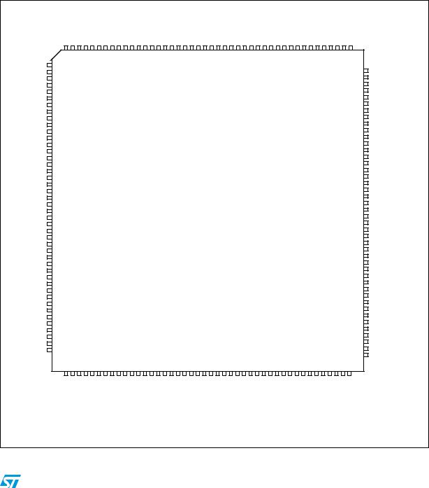
3 Package pinouts and signal descriptions
3.1Package pinouts
The available LQFP pinouts and the ballmap are provided in the following figures. For pin signal descriptions, please see Table 6.
Figure 2 shows the SPC560B54/6 in the LQFP176 package.
Figure 2. LQFP176 pin configuration
|
PB[2] PC[8] PC[13] PC[12] PI[0] |
PI[1] |
PI[2] |
PI[3] |
PE[7] |
PE[6] |
PH[8] |
PH[7] |
PH[6] |
PH[5] |
PH[4] PE[5] PE[4] PC[4] PC[5] |
PE[3] PE[2] PH[9] PC[0] VSS LV |
VDD LV |
VDD HV |
VSS HV |
PC[1] |
PH[10] |
PA[6] |
PA[5] |
PC[2] |
PC[3] PI[4] PI[5] PH[12] PH[11] |
PG[11] |
PG[10] |
PE[15] |
PE[14] |
PG[15] |
PG[14] |
PE[12] |
|
||||||||||||||||
PB[3] |
176 |
175 |
174 |
173 |
172 |
171 |
170 |
169 |
168 |
167 |
166 |
165 |
164 |
163 |
162 |
161 |
160 |
159 |
158 |
157 |
156 |
155 |
154 |
153 |
152 |
151 |
150 |
149 |
148 |
147 |
146 |
145 |
144 |
143 |
142 |
141 |
140 |
139 |
138 |
137 |
136 |
135 |
134 |
133 |
|
1 |
|
|
|
|
|
|
|
|
|
|
|
|
|
|
|
|
|
|
|
|
|
|
|
|
|
|
|
|
|
|
|
|
|
|
|
|
|
|
|
|
|
|
132 |
PA[11] |
|
PC[9] |
2 |
|
|
|
|
|
|
|
|
|
|
|
|
|
|
|
|
|
|
|
|
|
|
|
|
|
|
|
|
|
|
|
|
|
|
|
|
|
|
|
|
|
|
||
PC[14] |
3 |
|
|
|
|
|
|
|
|
|
|
|
|
|
|
|
|
|
|
|
|
|
|
|
|
|
|
|
|
|
|
|
|
|
|
|
|
|
|
|
|
|
|
131 |
PA[10] |
PC[15] |
4 |
|
|
|
|
|
|
|
|
|
|
|
|
|
|
|
|
|
|
|
|
|
|
|
|
|
|
|
|
|
|
|
|
|
|
|
|
|
|
|
|
|
|
130 |
PA[9] |
PJ[4] |
5 |
|
|
|
|
|
|
|
|
|
|
|
|
|
|
|
|
|
|
|
|
|
|
|
|
|
|
|
|
|
|
|
|
|
|
|
|
|
|
|
|
|
|
129 |
PA[8] |
VDD_HV |
6 |
|
|
|
|
|
|
|
|
|
|
|
|
|
|
|
|
|
|
|
|
|
|
|
|
|
|
|
|
|
|
|
|
|
|
|
|
|
|
|
|
|
|
128 |
PA[7] |
VSS_HV |
7 |
|
|
|
|
|
|
|
|
|
|
|
|
|
|
|
|
|
|
|
|
|
|
|
|
|
|
|
|
|
|
|
|
|
|
|
|
|
|
|
|
|
|
127 |
PE[13] |
PH[15] |
8 |
|
|
|
|
|
|
|
|
|
|
|
|
|
|
|
|
|
|
|
|
|
|
|
|
|
|
|
|
|
|
|
|
|
|
|
|
|
|
|
|
|
|
126 |
PF[14] |
PH[13] |
9 |
|
|
|
|
|
|
|
|
|
|
|
|
|
|
|
|
|
|
|
|
|
|
|
|
|
|
|
|
|
|
|
|
|
|
|
|
|
|
|
|
|
|
125 |
PF[15] |
PH[14] |
10 |
|
|
|
|
|
|
|
|
|
|
|
|
|
|
|
|
|
|
|
|
|
|
|
|
|
|
|
|
|
|
|
|
|
|
|
|
|
|
|
|
|
|
124 |
VDD_HV |
PI[6] |
11 |
|
|
|
|
|
|
|
|
|
|
|
|
|
|
|
|
|
|
|
|
|
|
|
|
|
|
|
|
|
|
|
|
|
|
|
|
|
|
|
|
|
|
123 |
VSS_HV |
PI[7] |
12 |
|
|
|
|
|
|
|
|
|
|
|
|
|
|
|
|
|
|
|
|
|
|
|
|
|
|
|
|
|
|
|
|
|
|
|
|
|
|
|
|
|
|
122 |
PG[0] |
PG[5] |
13 |
|
|
|
|
|
|
|
|
|
|
|
|
|
|
|
|
|
|
|
|
|
|
|
|
|
|
|
|
|
|
|
|
|
|
|
|
|
|
|
|
|
|
121 |
PG[1] |
PG[4] |
14 |
|
|
|
|
|
|
|
|
|
|
|
|
|
|
|
|
|
|
|
|
|
|
|
|
|
|
|
|
|
|
|
|
|
|
|
|
|
|
|
|
|
|
120 |
PH[3] |
PG[3] |
15 |
|
|
|
|
|
|
|
|
|
|
|
|
|
|
|
|
|
|
|
|
|
|
|
|
|
|
|
|
|
|
|
|
|
|
|
|
|
|
|
|
|
|
119 |
PH[2] |
PG[2] |
16 |
|
|
|
|
|
|
|
|
|
|
|
|
|
|
|
|
|
|
|
|
|
|
|
|
|
|
|
|
|
|
|
|
|
|
|
|
|
|
|
|
|
|
118 |
PH[1] |
PA[2] |
17 |
|
|
|
|
|
|
|
|
|
|
|
|
|
|
|
|
|
|
|
|
|
|
|
|
|
|
|
|
|
|
|
|
|
|
|
|
|
|
|
|
|
|
117 |
PH[0] |
PE[0] |
18 |
|
|
|
|
|
|
|
|
|
|
|
|
|
|
|
|
|
|
|
|
|
|
|
|
|
|
|
|
|
|
|
|
|
|
|
|
|
|
|
|
|
|
116 |
PG[12] |
PA[1] |
19 |
|
|
|
|
|
|
|
|
|
|
|
|
|
|
|
|
|
|
|
|
|
|
|
|
|
|
|
|
|
|
|
|
|
|
|
|
|
|
|
|
|
|
115 |
PG[13] |
PE[1] |
20 |
|
|
|
|
|
|
|
|
|
|
|
|
|
|
|
|
|
|
|
|
|
|
|
|
|
|
|
|
|
|
|
|
|
|
|
|
|
|
|
|
|
|
114 |
PA[3] |
PE[8] |
21 |
|
|
|
|
|
|
|
|
|
|
|
|
|
|
|
|
|
|
|
|
|
|
|
|
|
|
|
|
|
|
|
|
|
|
|
|
|
|
|
|
|
|
113 |
PI[13] |
PE[9] |
22 |
|
|
|
|
|
|
|
|
|
|
|
|
|
|
|
|
|
|
LQFP176 |
|
|
|
|
|
|
|
|
|
|
|
|
|
|
|
|
|
112 |
PI[12] |
||||||
|
|
|
|
|
|
|
|
|
|
|
|
|
|
|
|
|
|
|
|
|
|
|
|
|
|
|
|
|
|
|
|
|
|
|
111 |
PI[11] |
|||||||||
PE[10] |
23 |
|
|
|
|
|
|
|
|
|
|
|
|
|
|
|
|
|
|
|
|
|
|
|
|
|
|
|
|
|
|
|
|
|
|
|
|
|
|
|
|
|
|
||
PA[0] |
24 |
|
|
|
|
|
|
|
|
|
|
|
|
|
|
|
|
|
|
|
Top view |
|
|
|
|
|
|
|
|
|
|
|
|
|
|
|
|
|
|
110 |
PI[10] |
||||
PE[11] |
25 |
|
|
|
|
|
|
|
|
|
|
|
|
|
|
|
|
|
|
|
|
|
|
|
|
|
|
|
|
|
|
|
|
|
|
|
|
|
109 |
PI[9] |
|||||
VSS_HV |
26 |
|
|
|
|
|
|
|
|
|
|
|
|
|
|
|
|
|
|
|
|
|
|
|
|
|
|
|
|
|
|
|
|
|
|
|
|
|
|
|
|
|
|
108 |
PI[8] |
VDD_HV |
27 |
|
|
|
|
|
|
|
|
|
|
|
|
|
|
|
|
|
|
|
|
|
|
|
|
|
|
|
|
|
|
|
|
|
|
|
|
|
|
|
|
|
|
107 |
PB[15] |
VSS_HV |
28 |
|
|
|
|
|
|
|
|
|
|
|
|
|
|
|
|
|
|
|
|
|
|
|
|
|
|
|
|
|
|
|
|
|
|
|
|
|
|
|
|
|
|
106 |
PD[15] |
RESET |
29 |
|
|
|
|
|
|
|
|
|
|
|
|
|
|
|
|
|
|
|
|
|
|
|
|
|
|
|
|
|
|
|
|
|
|
|
|
|
|
|
|
|
|
105 |
PB[14] |
VSS_LV |
30 |
|
|
|
|
|
|
|
|
|
|
|
|
|
|
|
|
|
|
|
|
|
|
|
|
|
|
|
|
|
|
|
|
|
|
|
|
|
|
|
|
|
|
104 |
PD[14] |
VDD_LV |
31 |
|
|
|
|
|
|
|
|
|
|
|
|
|
|
|
|
|
|
|
|
|
|
|
|
|
|
|
|
|
|
|
|
|
|
|
|
|
|
|
|
|
|
103 |
PB[13] |
VDD_BV |
32 |
|
|
|
|
|
|
|
|
|
|
|
|
|
|
|
|
|
|
|
|
|
|
|
|
|
|
|
|
|
|
|
|
|
|
|
|
|
|
|
|
|
|
102 |
PD[13] |
PG[9] |
33 |
|
|
|
|
|
|
|
|
|
|
|
|
|
|
|
|
|
|
|
|
|
|
|
|
|
|
|
|
|
|
|
|
|
|
|
|
|
|
|
|
|
|
101 |
PB[12] |
PG[8] |
34 |
|
|
|
|
|
|
|
|
|
|
|
|
|
|
|
|
|
|
|
|
|
|
|
|
|
|
|
|
|
|
|
|
|
|
|
|
|
|
|
|
|
|
100 |
PD[12] |
PC[11] |
35 |
|
|
|
|
|
|
|
|
|
|
|
|
|
|
|
|
|
|
|
|
|
|
|
|
|
|
|
|
|
|
|
|
|
|
|
|
|
|
|
|
|
|
99 |
VDD_HV_ADC1 |
PC[10] |
36 |
|
|
|
|
|
|
|
|
|
|
|
|
|
|
|
|
|
|
|
|
|
|
|
|
|
|
|
|
|
|
|
|
|
|
|
|
|
|
|
|
|
|
98 |
VSS_HV_ADC1 |
|
|
|
|
|
|
|
|
|
|
|
|
|
|
|
|
|
|
|
|
|
|
|
|
|
|
|
|
|
|
|
|
|
|
|
|
|
|
|
|
|
|
97 |
PB[11] |
||
PG[7] |
37 |
|
|
|
|
|
|
|
|
|
|
|
|
|
|
|
|
|
|
|
|
|
|
|
|
|
|
|
|
|
|
|
|
|
|
|
|
|
|
|
|
|
|
||
|
|
|
|
|
|
|
|
|
|
|
|
|
|
|
|
|
|
|
|
|
|
|
|
|
|
|
|
|
|
|
|
|
|
|
|
|
|
|
|
|
|
96 |
PD[11] |
||
PG[6] |
38 |
|
|
|
|
|
|
|
|
|
|
|
|
|
|
|
|
|
|
|
|
|
|
|
|
|
|
|
|
|
|
|
|
|
|
|
|
|
|
|
|
|
|
||
PB[0] |
39 |
|
|
|
|
|
|
|
|
|
|
|
|
|
|
|
|
|
|
|
|
|
|
|
|
|
|
|
|
|
|
|
|
|
|
|
|
|
|
|
|
|
|
95 |
PD[10] |
PB[1] |
40 |
|
|
|
|
|
|
|
|
|
|
|
|
|
|
|
|
|
|
|
|
|
|
|
|
|
|
|
|
|
|
|
|
|
|
|
|
|
|
|
|
|
|
94 |
PD[9] |
PF[9] |
41 |
|
|
|
|
|
|
|
|
|
|
|
|
|
|
|
|
|
|
|
|
|
|
|
|
|
|
|
|
|
|
|
|
|
|
|
|
|
|
|
|
|
|
93 |
PB[7] |
PF[8] |
42 |
|
|
|
|
|
|
|
|
|
|
|
|
|
|
|
|
|
|
|
|
|
|
|
|
|
|
|
|
|
|
|
|
|
|
|
|
|
|
|
|
|
|
92 |
PB[6] |
|
|
|
|
|
|
|
|
|
|
|
|
|
|
|
|
|
|
|
|
|
|
|
|
|
|
|
|
|
|
|
|
|
|
|
|
|
|
|
|
|
|
91 |
PB[5] |
||
PF[12] |
43 |
|
|
|
|
|
|
|
|
|
|
|
|
|
|
|
|
|
|
|
|
|
|
|
|
|
|
|
|
|
|
|
|
|
|
|
|
|
|
|
|
|
|
||
|
|
|
|
|
|
|
|
|
|
|
|
|
|
|
|
|
|
|
|
|
|
|
|
|
|
|
|
|
|
|
|
|
|
|
|
|
|
|
|
|
|
90 |
VDD_HV_ADC0 |
||
PC[6] |
44 |
|
|
|
|
|
|
|
|
|
|
|
|
|
|
|
|
|
|
|
|
|
|
|
|
|
|
|
|
|
|
|
|
|
|
|
|
|
|
|
|
|
|
||
|
|
|
|
|
|
|
|
|
|
|
|
|
|
|
|
|
|
|
|
|
|
|
|
|
|
|
|
|
|
|
|
|
|
|
|
|
|
|
|
|
|
|
|
89 |
VSS_HV_ADC0 |
|
45 |
46 |
47 |
48 |
49 |
50 |
51 |
52 |
53 |
54 |
55 |
56 |
57 |
58 |
59 |
60 |
61 |
62 |
63 |
64 |
65 |
66 |
67 |
68 |
69 |
70 |
71 |
72 |
73 |
74 |
75 |
76 |
77 |
78 |
79 |
80 |
81 |
82 |
83 |
84 |
85 |
86 |
87 |
88 |
|
|
PC[7] |
PF[10] |
PF[11] |
PA[15] |
PF[13] |
PA[14] |
PA[4] |
PA[13] |
PA[12] |
VDD LV |
VSS LV |
XTAL |
VSS HV |
EXTAL |
VDD HV |
PB[9] |
PB[8] |
PB[10] |
PF[0] |
PF[1] |
PF[2] |
PF[3] |
PF[4] |
PF[5] |
PF[6] |
PF[7] |
PJ[3] |
PJ[2] |
PJ[1] |
PJ[0] |
PI[15] |
PI[14] |
PD[0] |
PD[1] |
PD[2] |
PD[3] |
PD[4] |
PD[5] |
PD[6] |
PD[7] |
VDD HV |
VSS HV |
PD[8] |
PB[4] |
|
Doc ID 15131 Rev 6 |
13/134 |

Package pinouts and signal descriptions |
SPC560B54/6x |
|
|
Figure 3 shows the SPC560B54/6 in the LQFP144 package.
Figure 3. LQFP144 pin configuration
|
|
|
|
PB[2] |
PC[8] |
PC[13] |
PC[12] |
PE[7] |
PE[6] |
PH[8] |
PH[7] |
PH[6] |
PH[5] |
PH[4] |
PE[5] |
PE[4] |
PC[4] |
PC[5] |
PE[3] |
PE[2] |
PH[9] |
PC[0] |
VSS_LV |
VDD_LV |
VDD_HV |
VSS_HV |
PC[1] |
PH[10] |
PA[6] |
PA[5] |
PC[2] |
PC[3] |
PG[11] |
PG[10] |
PE[15] |
PE[14] |
PG[15] |
PG[14] |
PE[12] |
|
|
|
||||||||||||||||||||||||||||||||||||||||||||||||||||||||||||||||
|
|
|
|
|
|
|
|
|
|
|
|
|
|
|
|
|
|
|
|
|
|
|
|
|
|
|
|
|
|
|
|
|
|
|
|
|
|
|
|
|
|
|
|
|
|
|
|
|
|
|
|
|
|
|
|
|
|
|
|
|
|
|
|
|
|
|
|
|
|
|
|
|
|
|
|
|
|
|
|
|
|
|
|
|
|
|
|
|
|
|
|
|
|
|
|
|
|
|
|
|
|
|
|
|
|
|
|
|
144 |
|
143 |
|
142 |
|
141 |
|
140 |
139 |
|
138 |
|
137 |
|
136 |
|
135 |
|
134 |
|
133 |
|
132 |
|
131 |
|
130 |
|
129 |
128 |
|
127 |
|
126 |
|
125 |
|
124 |
|
123 |
|
122 |
|
121 |
|
120 |
|
119 |
|
118 |
117 |
|
116 |
|
115 |
114 |
113 |
112 |
111 |
110 |
109 |
|
|
|
|
|||||||||||||||||||||||||||||||||||||||
PB[3] |
|
|
1 |
|
|
|
|
|
|
|
|
|
|
|
|
|
|
|
|
|
|
|
|
|
|
|
|
|
|
|
|
|
|
|
|
|
|
|
|
|
|
|
|
|
|
|
|
|
|
|
|
|
|
|
|
|
|
|
|
|
|
|
|
|
|
|
|
|
|
|
|
|
|
|
|
|
|
|
|
|
|
|
|
|
|
|
|
|
|
|
|
|
|
|
|
|
|
|
|
|
108 |
|
|
PA[11] |
||
PC[9] |
|
|
2 |
|
|
|
|
|
|
|
|
|
|
|
|
|
|
|
|
|
|
|
|
|
|
|
|
|
|
|
|
|
|
|
|
|
|
|
|
|
|
|
|
|
|
|
|
|
|
|
|
|
|
|
|
|
|
|
|
|
|
|
|
|
|
|
|
|
|
|
|
|
|
|
|
|
|
|
|
|
|
|
|
|
|
|
|
|
|
|
|
|
|
|
|
|
|
|
|
|
107 |
|
|
PA[10] |
||
PC[14] |
|
|
3 |
|
|
|
|
|
|
|
|
|
|
|
|
|
|
|
|
|
|
|
|
|
|
|
|
|
|
|
|
|
|
|
|
|
|
|
|
|
|
|
|
|
|
|
|
|
|
|
|
|
|
|
|
|
|
|
|
|
|
|
|
|
|
|
|
|
|
|
|
|
|
|
|
|
|
|
|
|
|
|
|
|
|
|
|
|
|
|
|
|
|
|
|
|
|
|
|
|
106 |
|
|
PA[9] |
||
PC[15] |
|
|
4 |
|
|
|
|
|
|
|
|
|
|
|
|
|
|
|
|
|
|
|
|
|
|
|
|
|
|
|
|
|
|
|
|
|
|
|
|
|
|
|
|
|
|
|
|
|
|
|
|
|
|
|
|
|
|
|
|
|
|
|
|
|
|
|
|
|
|
|
|
|
|
|
|
|
|
|
|
|
|
|
|
|
|
|
|
|
|
|
|
|
|
|
|
|
|
|
|
|
105 |
|
|
PA[8] |
||
PG[5] |
|
|
5 |
|
|
|
|
|
|
|
|
|
|
|
|
|
|
|
|
|
|
|
|
|
|
|
|
|
|
|
|
|
|
|
|
|
|
|
|
|
|
|
|
|
|
|
|
|
|
|
|
|
|
|
|
|
|
|
|
|
|
|
|
|
|
|
|
|
|
|
|
|
|
|
|
|
|
|
|
|
|
|
|
|
|
|
|
|
|
|
|
|
|
|
|
|
|
|
|
|
104 |
|
|
PA[7] |
||
PG[4] |
|
|
6 |
|
|
|
|
|
|
|
|
|
|
|
|
|
|
|
|
|
|
|
|
|
|
|
|
|
|
|
|
|
|
|
|
|
|
|
|
|
|
|
|
|
|
|
|
|
|
|
|
|
|
|
|
|
|
|
|
|
|
|
|
|
|
|
|
|
|
|
|
|
|
|
|
|
|
|
|
|
|
|
|
|
|
|
|
|
|
|
|
|
|
|
|
|
|
|
|
|
103 |
|
|
PE[13] |
||
PG[3] |
|
|
7 |
|
|
|
|
|
|
|
|
|
|
|
|
|
|
|
|
|
|
|
|
|
|
|
|
|
|
|
|
|
|
|
|
|
|
|
|
|
|
|
|
|
|
|
|
|
|
|
|
|
|
|
|
|
|
|
|
|
|
|
|
|
|
|
|
|
|
|
|
|
|
|
|
|
|
|
|
|
|
|
|
|
|
|
|
|
|
|
|
|
|
|
|
|
|
|
|
|
102 |
|
|
PF[14] |
||
PG[2] |
|
|
8 |
|
|
|
|
|
|
|
|
|
|
|
|
|
|
|
|
|
|
|
|
|
|
|
|
|
|
|
|
|
|
|
|
|
|
|
|
|
|
|
|
|
|
|
|
|
|
|
|
|
|
|
|
|
|
|
|
|
|
|
|
|
|
|
|
|
|
|
|
|
|
|
|
|
|
|
|
|
|
|
|
|
|
|
|
|
|
|
|
|
|
|
|
|
|
|
|
|
101 |
|
|
PF[15] |
||
PA[2] |
|
|
9 |
|
|
|
|
|
|
|
|
|
|
|
|
|
|
|
|
|
|
|
|
|
|
|
|
|
|
|
|
|
|
|
|
|
|
|
|
|
|
|
|
|
|
|
|
|
|
|
|
|
|
|
|
|
|
|
|
|
|
|
|
|
|
|
|
|
|
|
|
|
|
|
|
|
|
|
|
|
|
|
|
|
|
|
|
|
|
|
|
|
|
|
|
|
|
|
|
|
100 |
|
|
VDD_HV |
||
PE[0] |
|
|
10 |
|
|
|
|
|
|
|
|
|
|
|
|
|
|
|
|
|
|
|
|
|
|
|
|
|
|
|
|
|
|
|
|
|
|
|
|
|
|
|
|
|
|
|
|
|
|
|
|
|
|
|
|
|
|
|
|
|
|
|
|
|
|
|
|
|
|
|
|
|
|
|
|
|
|
|
|
|
|
|
|
|
|
|
|
|
|
|
|
|
|
|
|
|
|
|
|
|
99 |
|
|
VSS_HV |
||
PA[1] |
|
|
11 |
|
|
|
|
|
|
|
|
|
|
|
|
|
|
|
|
|
|
|
|
|
|
|
|
|
|
|
|
|
|
|
|
|
|
|
|
|
|
|
|
|
|
|
|
|
|
|
|
|
|
|
|
|
|
|
|
|
|
|
|
|
|
|
|
|
|
|
|
|
|
|
|
|
|
|
|
|
|
|
|
|
|
|
|
|
|
|
|
|
|
|
|
|
|
|
|
|
98 |
|
|
PG[0] |
||
PE[1] |
|
|
12 |
|
|
|
|
|
|
|
|
|
|
|
|
|
|
|
|
|
|
|
|
|
|
|
|
|
|
|
|
|
|
|
|
|
|
|
|
|
|
|
|
|
|
|
|
|
|
|
|
|
|
|
|
|
|
|
|
|
|
|
|
|
|
|
|
|
|
|
|
|
|
|
|
|
|
|
|
|
|
|
|
|
|
|
|
|
|
|
|
|
|
|
|
|
|
|
|
|
97 |
|
|
PG[1] |
||
PE[8] |
|
|
13 |
|
|
|
|
|
|
|
|
|
|
|
|
|
|
|
|
|
|
|
|
|
|
|
|
|
|
|
|
|
|
|
|
|
|
|
|
|
|
|
|
|
|
|
|
|
|
|
|
|
|
|
|
|
|
|
|
|
|
|
|
|
|
|
|
|
|
|
|
|
|
|
|
|
|
|
|
|
|
|
|
|
|
|
|
|
|
|
|
|
|
|
|
|
|
|
|
|
96 |
|
|
PH[3] |
||
PE[9] |
|
|
14 |
|
|
|
|
|
|
|
|
|
|
|
|
|
|
|
|
|
|
|
|
|
|
|
|
|
|
|
|
|
|
|
|
|
|
|
|
|
|
|
|
|
|
|
|
|
|
|
|
|
|
|
|
|
|
|
|
|
|
|
|
|
|
|
|
|
|
|
|
|
|
|
|
|
|
|
|
|
|
|
|
|
|
|
|
|
|
|
|
|
|
|
|
|
|
|
|
|
95 |
|
|
PH[2] |
||
PE[10] |
|
|
15 |
|
|
|
|
|
|
|
|
|
|
|
|
|
|
|
|
|
|
|
|
|
|
|
|
|
|
|
|
|
|
|
|
|
|
|
|
|
|
|
|
|
|
|
|
|
|
|
|
|
|
|
|
|
|
|
|
|
|
|
|
|
|
|
|
|
|
|
|
|
|
|
|
|
|
|
|
|
|
|
|
|
|
|
|
|
|
|
|
|
|
|
|
|
|
|
|
|
94 |
|
|
PH[1] |
||
PA[0] |
|
|
16 |
|
|
|
|
|
|
|
|
|
|
|
|
|
|
|
|
|
|
|
|
|
|
|
|
|
|
|
|
|
|
|
|
|
|
|
|
|
|
|
|
|
|
|
|
|
|
|
|
|
|
|
|
|
|
|
|
|
|
|
|
|
|
|
|
|
|
|
|
|
|
|
|
|
|
|
|
|
|
|
|
|
|
|
|
|
|
|
|
|
|
|
|
|
|
|
|
|
93 |
|
|
PH[0] |
||
PE[11] |
|
|
17 |
|
|
|
|
|
|
|
|
|
|
|
|
|
|
|
|
|
|
|
|
|
|
|
|
|
|
|
|
|
|
|
|
|
|
|
|
|
|
|
|
|
|
|
|
|
|
LQFP144 |
|
|
|
|
|
|
|
|
|
|
|
|
|
|
|
|
|
|
|
|
|
|
|
|
|
|
|
|
|
|
|
|
|
|
|
92 |
|
|
PG[12] |
|||||||||||||||||
VSS_HV |
|
|
18 |
|
|
|
|
|
|
|
|
|
|
|
|
|
|
|
|
|
|
|
|
|
|
|
|
|
|
|
|
|
|
|
|
|
|
|
|
|
|
|
|
|
|
|
|
|
|
|
|
|
|
|
|
|
|
|
|
|
|
|
|
|
|
|
|
|
|
|
|
|
|
|
|
|
|
|
|
|
|
|
|
|
91 |
|
|
PG[13] |
||||||||||||||||||
VDD_HV |
|
|
19 |
|
|
|
|
|
|
|
|
|
|
|
|
|
|
|
|
|
|
|
|
|
|
|
|
|
|
|
|
|
|
|
|
|
|
|
|
|
|
|
|
|
|
|
|
|
|
|
|
|
|
|
|
|
|
|
|
|
|
|
|
|
|
|
|
|
|
|
|
|
|
|
|
|
|
|
|
|
|
|
|
|
|
|
|
|
|
|
|
|
|
|
|
|
|
|
|
|
90 |
|
|
PA[3] |
||
VSS_HV |
|
|
20 |
|
|
|
|
|
|
|
|
|
|
|
|
|
|
|
|
|
|
|
|
|
|
|
|
|
|
|
|
|
|
|
|
|
|
|
|
|
|
|
|
|
|
|
|
|
|
|
Top view |
|
|
|
|
|
|
|
|
|
|
|
|
|
|
|
|
|
|
|
|
|
|
|
|
|
|
|
|
|
|
|
|
|
|
|
89 |
|
|
PB[15] |
||||||||||||||||
RESET |
|
|
21 |
|
|
|
|
|
|
|
|
|
|
|
|
|
|
|
|
|
|
|
|
|
|
|
|
|
|
|
|
|
|
|
|
|
|
|
|
|
|
|
|
|
|
|
|
|
|
|
|
|
|
|
|
|
|
|
|
|
|
|
|
|
|
|
|
|
|
|
|
|
|
|
|
|
|
|
|
|
|
|
|
|
|
88 |
|
|
PD[15] |
|||||||||||||||||
VSS_LV |
|
|
22 |
|
|
|
|
|
|
|
|
|
|
|
|
|
|
|
|
|
|
|
|
|
|
|
|
|
|
|
|
|
|
|
|
|
|
|
|
|
|
|
|
|
|
|
|
|
|
|
|
|
|
|
|
|
|
|
|
|
|
|
|
|
|
|
|
|
|
|
|
|
|
|
|
|
|
|
|
|
|
|
|
|
|
|
|
|
|
|
|
|
|
|
|
|
|
|
|
|
87 |
|
|
PB[14] |
||
VDD_LV |
|
|
23 |
|
|
|
|
|
|
|
|
|
|
|
|
|
|
|
|
|
|
|
|
|
|
|
|
|
|
|
|
|
|
|
|
|
|
|
|
|
|
|
|
|
|
|
|
|
|
|
|
|
|
|
|
|
|
|
|
|
|
|
|
|
|
|
|
|
|
|
|
|
|
|
|
|
|
|
|
|
|
|
|
|
|
|
|
|
|
|
|
|
|
|
|
|
|
|
|
|
86 |
|
|
PD[14] |
||
VDD_BV |
|
|
24 |
|
|
|
|
|
|
|
|
|
|
|
|
|
|
|
|
|
|
|
|
|
|
|
|
|
|
|
|
|
|
|
|
|
|
|
|
|
|
|
|
|
|
|
|
|
|
|
|
|
|
|
|
|
|
|
|
|
|
|
|
|
|
|
|
|
|
|
|
|
|
|
|
|
|
|
|
|
|
|
|
|
|
|
|
|
|
|
|
|
|
|
|
|
|
|
|
|
85 |
|
|
PB[13] |
||
PG[9] |
|
|
25 |
|
|
|
|
|
|
|
|
|
|
|
|
|
|
|
|
|
|
|
|
|
|
|
|
|
|
|
|
|
|
|
|
|
|
|
|
|
|
|
|
|
|
|
|
|
|
|
|
|
|
|
|
|
|
|
|
|
|
|
|
|
|
|
|
|
|
|
|
|
|
|
|
|
|
|
|
|
|
|
|
|
|
|
|
|
|
|
|
|
|
|
|
|
|
|
|
|
84 |
|
|
PD[13] |
||
PG[8] |
|
|
26 |
|
|
|
|
|
|
|
|
|
|
|
|
|
|
|
|
|
|
|
|
|
|
|
|
|
|
|
|
|
|
|
|
|
|
|
|
|
|
|
|
|
|
|
|
|
|
|
|
|
|
|
|
|
|
|
|
|
|
|
|
|
|
|
|
|
|
|
|
|
|
|
|
|
|
|
|
|
|
|
|
|
|
|
|
|
|
|
|
|
|
|
|
|
|
|
|
|
83 |
|
|
PB[12] |
||
PC[11] |
|
|
27 |
|
|
|
|
|
|
|
|
|
|
|
|
|
|
|
|
|
|
|
|
|
|
|
|
|
|
|
|
|
|
|
|
|
|
|
|
|
|
|
|
|
|
|
|
|
|
|
|
|
|
|
|
|
|
|
|
|
|
|
|
|
|
|
|
|
|
|
|
|
|
|
|
|
|
|
|
|
|
|
|
|
|
|
|
|
|
|
|
|
|
|
|
|
|
|
|
|
82 |
|
|
VDD_HV_ADC1 |
||
PC[10] |
|
|
28 |
|
|
|
|
|
|
|
|
|
|
|
|
|
|
|
|
|
|
|
|
|
|
|
|
|
|
|
|
|
|
|
|
|
|
|
|
|
|
|
|
|
|
|
|
|
|
|
|
|
|
|
|
|
|
|
|
|
|
|
|
|
|
|
|
|
|
|
|
|
|
|
|
|
|
|
|
|
|
|
|
|
|
|
|
|
|
|
|
|
|
|
|
|
|
|
|
|
81 |
|
|
VSS_HV_ADC1 |
||
PG[7] |
|
|
29 |
|
|
|
|
|
|
|
|
|
|
|
|
|
|
|
|
|
|
|
|
|
|
|
|
|
|
|
|
|
|
|
|
|
|
|
|
|
|
|
|
|
|
|
|
|
|
|
|
|
|
|
|
|
|
|
|
|
|
|
|
|
|
|
|
|
|
|
|
|
|
|
|
|
|
|
|
|
|
|
|
|
|
|
|
|
|
|
|
|
|
|
|
|
|
|
|
|
80 |
|
|
PD[11] |
||
PG[6] |
|
|
30 |
|
|
|
|
|
|
|
|
|
|
|
|
|
|
|
|
|
|
|
|
|
|
|
|
|
|
|
|
|
|
|
|
|
|
|
|
|
|
|
|
|
|
|
|
|
|
|
|
|
|
|
|
|
|
|
|
|
|
|
|
|
|
|
|
|
|
|
|
|
|
|
|
|
|
|
|
|
|
|
|
|
|
|
|
|
|
|
|
|
|
|
|
|
|
|
|
|
79 |
|
|
PD[10] |
||
PB[0] |
|
|
31 |
|
|
|
|
|
|
|
|
|
|
|
|
|
|
|
|
|
|
|
|
|
|
|
|
|
|
|
|
|
|
|
|
|
|
|
|
|
|
|
|
|
|
|
|
|
|
|
|
|
|
|
|
|
|
|
|
|
|
|
|
|
|
|
|
|
|
|
|
|
|
|
|
|
|
|
|
|
|
|
|
|
|
|
|
|
|
|
|
|
|
|
|
|
|
|
|
|
78 |
|
|
PD[9] |
||
PB[1] |
|
|
32 |
|
|
|
|
|
|
|
|
|
|
|
|
|
|
|
|
|
|
|
|
|
|
|
|
|
|
|
|
|
|
|
|
|
|
|
|
|
|
|
|
|
|
|
|
|
|
|
|
|
|
|
|
|
|
|
|
|
|
|
|
|
|
|
|
|
|
|
|
|
|
|
|
|
|
|
|
|
|
|
|
|
|
|
|
|
|
|
|
|
|
|
|
|
|
|
|
|
77 |
|
|
PB[7] |
||
PF[9] |
|
|
33 |
|
|
|
|
|
|
|
|
|
|
|
|
|
|
|
|
|
|
|
|
|
|
|
|
|
|
|
|
|
|
|
|
|
|
|
|
|
|
|
|
|
|
|
|
|
|
|
|
|
|
|
|
|
|
|
|
|
|
|
|
|
|
|
|
|
|
|
|
|
|
|
|
|
|
|
|
|
|
|
|
|
|
|
|
|
|
|
|
|
|
|
|
|
|
|
|
|
76 |
|
|
PB[6] |
||
PF[8] |
|
|
34 |
|
|
|
|
|
|
|
|
|
|
|
|
|
|
|
|
|
|
|
|
|
|
|
|
|
|
|
|
|
|
|
|
|
|
|
|
|
|
|
|
|
|
|
|
|
|
|
|
|
|
|
|
|
|
|
|
|
|
|
|
|
|
|
|
|
|
|
|
|
|
|
|
|
|
|
|
|
|
|
|
|
|
|
|
|
|
|
|
|
|
|
|
|
|
|
|
|
75 |
|
|
PB[5] |
||
PF[12] |
|
|
35 |
|
|
|
|
|
|
|
|
|
|
|
|
|
|
|
|
|
|
|
|
|
|
|
|
|
|
|
|
|
|
|
|
|
|
|
|
|
|
|
|
|
|
|
|
|
|
|
|
|
|
|
|
|
|
|
|
|
|
|
|
|
|
|
|
|
|
|
|
|
|
|
|
|
|
|
|
|
|
|
|
|
|
|
|
|
|
|
|
|
|
|
|
|
|
|
|
|
74 |
|
|
VDD_HV_ADC0 |
||
PC[6] |
|
|
36 |
|
|
|
|
|
|
|
|
|
|
|
|
|
|
|
|
|
|
|
|
|
|
|
|
|
|
|
|
|
|
|
|
|
|
|
|
|
|
|
|
|
|
|
|
|
|
|
|
|
|
|
|
|
|
|
|
|
|
|
|
|
|
|
|
|
|
|
|
|
|
|
|
|
|
|
|
|
|
|
|
|
|
|
|
|
|
|
|
|
|
|
|
|
|
|
|
|
73 |
|
|
VSS_HV_ADC0 |
||
|
|
37 |
|
38 |
|
39 |
|
40 |
|
41 |
42 |
|
43 |
|
44 |
|
45 |
|
46 |
|
47 |
|
48 |
|
49 |
|
50 |
|
51 |
|
52 |
53 |
|
54 |
|
55 |
|
56 |
|
57 |
|
58 |
|
59 |
|
60 |
|
61 |
|
62 |
|
63 |
64 |
|
65 |
|
66 |
67 |
68 |
69 |
70 |
71 |
72 |
|
|
|
|
|||||||||||||||||||||||||||||||||||||||
|
|
|
|
|
|
|
|
|
|
|
|
|
|
|
|
|
|
|
|
|
|
|
|
|
|
|
|
|
|
|
|
|
|
|
|
|
|
|
|
|
|
|
|
|
|
|
|
|
|
|
|
|
|
|
|
|
|
|
|
|
||||||||||||||||||||||||||||||||||||||||||||||
|
|
|
|
|
|
|
|
|
|
|
|
|
|
|
|
|
|
|
|
|
|
|
|
|
|
|
|
|
|
|
|
|
|
|
|
|
|
|
|
|
|
|
|
|
|
|
|
|
|
|
|
|
|
|
|
|
|
|
|
|
|
|
|
|
|
|
|
|
|
|
|
|
|
|
|
|
|
|
|
|
|
|
|
|
|
|
|
|
|
|
|
|
|
|
|
|
|
|
|
|
|
|
|
|
|
|
|
|
|
|
|
PC[7] |
|
PF[10] |
|
PF[11] |
|
PA[15] |
|
PF[13] |
|
PA[14] |
|
PA[4] |
|
PA[13] |
|
PA[12] |
|
VDD_LV |
|
VSS_LV |
|
XTAL |
|
VSS_HV |
|
EXTAL |
|
VDD_HV |
|
PB[9] |
|
PB[8] |
PB[10] |
PF[0] |
|
PF[1] |
PF[2] |
PF[3] |
PF[4] |
PF[5] |
PF[6] |
PF[7] |
PD[0] |
PD[1] |
PD[2] |
PD[3] |
PD[4] |
PD[5] |
PD[6] |
PD[7] |
PD[8] |
PB[4] |
|
|
|
||||||||||||||||||||||||||||||||||||||||||||||
|
|
|
|
|
|
|
|
|
|
|
|
|
|
|
|
|
|
|
|
|
|
|
|
|
|
|
|
|
|
|
|
|
|
|
|
|
|
|
|
|
|
|
|
|
|
|
|
|
|
|
|
|
|
|
|
|
|
|
|
|
|
|
|
|
|
|
|
|
|
|
|
|
|
|
|
|
|
|
|
|
|
|
|
|
|
|
|
|
|
|
|
|
|
|
|
|
|
|
|
|
|
|
|
|
|
|
Figure 4 shows the SPC560B54/6 in the LQFP100 package.
14/134 |
Doc ID 15131 Rev 6 |

SPC560B54/6x |
|
|
|
|
|
|
|
|
|
|
|
|
|
|
|
|
|
|
|
|
|
|
|
|
|
|
|
|
|
|
|
|
|
|
|
|
|
|
|
|
|
|
|
|
|
|
|
|
|
|
|
|
|
|
|
Package pinouts and signal descriptions |
|||||||||||||||||
|
|
|
|
|
|
|
|
|
|
|
|
|
|
|
|
|
|
|
|
|
|
|
|
|
|
|
|
|
|
|
|
|
|
|
|
|
|
|
|
|
|
|
|
|
|
|
|
|
|
|
|
|
|
|
|
|
|
|
|
|
|
|
|
|
|||||||||
Figure 4. |
LQFP100 pin configuration |
|
|
|
|
|
|
|
|
|
|
|
|
|
|
|
|
|
|
|
|
|
|
|
|
|
|
|
|
|
|
|
|
|
|
|
|
|
|
|
|
|
|
|
|||||||||||||||||||||||||||||
|
|
|
|
|
|
|
|
|
|
|
|
|
|
|
|
|
|
|
|
|
|
|
|
|
|
|
|
|
|
|
|
|
|
|
|
|
|
|
|
|
|
|
|||||||||||||||||||||||||||||||
|
|
|
|
|
PB[2] |
|
PC[8] |
|
PC[13] |
|
PC[12] |
|
PE[7] |
|
PE[6] |
|
PE[5] |
|
PE[4] |
|
PC[4] |
|
PC[5] |
|
PE[3] |
PE[2] |
PH[9] |
PC[0] |
VSS LV |
VDD LV |
VDD HV |
VSS HV |
PC[1] |
PH[10] |
PA[6] |
PA[5] |
PC[2] |
PC[3] |
PE[12] |
|
|
|
|||||||||||||||||||||||||||||||
|
|
|
|
|
|
|
|
|
|
|
|
|
|
|
|
|
|
|
|
|
|
|
|
|
|
|
|
|
|
|
|
|
|
|
|
|
|
|
|
|
|
|
|
|
|
|
|
|
|
|
|
|
|
|
|
|
|
|
|
|
|
|
|
|
|
|
|
|
|
|
|
|
|
|
|
|
|
|
|
|
|
|
|
|
|
|
|
|
|
|
|
|
|
|
|
|
|
|
|
|
|
|
|
|
|
|
|
|
|
|
|
|
|
|
|
|
|
|
|
|
|
|
|
|
|
|
|
|
|
|
|
|
|
|
|
|
|
|
|
|
|
|
|
|
|
|
|
|
|
|
100 |
99 |
98 |
97 |
96 |
95 |
94 |
93 |
92 |
91 |
90 |
89 |
88 |
87 |
|
86 |
|
85 |
|
84 |
|
83 |
82 |
81 |
80 |
79 |
78 |
77 |
76 |
|
|
|
|
||||||||||||||||||||||||||||||||||||||
|
PB[3] |
|
|
1 |
|
|
|
|
|
|
|
|
|
|
|
|
|
|
|
|
|
|
|
|
|
|
|
|
|
|
|
|
|
|
|
|
|
|
|
|
|
|
|
|
|
|
|
|
|
|
|
|
|
|
|
|
|
|
|
|
|
|
|
|
|
|
|
75 |
|
|
PA[11] |
||
|
|
|
|
|
|
|
|
|
|
|
|
|
|
|
|
|
|
|
|
|
|
|
|
|
|
|
|
|
|
|
|
|
|
|
|
|
|
|
|
|
|
|
|
|
|
|
|
|
|
|
|
|
|
|
|
|
|
|
|
|
|
|
|
|
|
|
|
||||||
|
PC[9] |
|
|
2 |
|
|
|
|
|
|
|
|
|
|
|
|
|
|
|
|
|
|
|
|
|
|
|
|
|
|
|
|
|
|
|
|
|
|
|
|
|
|
|
|
|
|
|
|
|
|
|
|
|
|
|
|
|
|
|
|
|
|
|
|
|
|
|
74 |
|
|
PA[10] |
||
|
|
|
|
|
|
|
|
|
|
|
|
|
|
|
|
|
|
|
|
|
|
|
|
|
|
|
|
|
|
|
|
|
|
|
|
|
|
|
|
|
|
|
|
|
|
|
|
|
|
|
|
|
|
|
|
|
|
|
|
|
|
|
|
|
|
|
|
||||||
|
PC[14] |
|
|
3 |
|
|
|
|
|
|
|
|
|
|
|
|
|
|
|
|
|
|
|
|
|
|
|
|
|
|
|
|
|
|
|
|
|
|
|
|
|
|
|
|
|
|
|
|
|
|
|
|
|
|
|
|
|
|
|
|
|
|
|
|
|
|
|
73 |
|
|
PA[9] |
||
|
|
|
|
|
|
|
|
|
|
|
|
|
|
|
|
|
|
|
|
|
|
|
|
|
|
|
|
|
|
|
|
|
|
|
|
|
|
|
|
|
|
|
|
|
|
|
|
|
|
|
|
|
|
|
|
|
|
|
|
|
|
|
|
|
|
|
|
||||||
|
PC[15] |
|
|
4 |
|
|
|
|
|
|
|
|
|
|
|
|
|
|
|
|
|
|
|
|
|
|
|
|
|
|
|
|
|
|
|
|
|
|
|
|
|
|
|
|
|
|
|
|
|
|
|
|
|
|
|
|
|
|
|
|
|
|
|
|
|
|
|
72 |
|
|
PA[8] |
||
|
|
|
|
|
|
|
|
|
|
|
|
|
|
|
|
|
|
|
|
|
|
|
|
|
|
|
|
|
|
|
|
|
|
|
|
|
|
|
|
|
|
|
|
|
|
|
|
|
|
|
|
|
|
|
|
|
|
|
|
|
|
|
|
|
|
|
|
||||||
|
PA[2] |
|
|
5 |
|
|
|
|
|
|
|
|
|
|
|
|
|
|
|
|
|
|
|
|
|
|
|
|
|
|
|
|
|
|
|
|
|
|
|
|
|
|
|
|
|
|
|
|
|
|
|
|
|
|
|
|
|
|
|
|
|
|
|
|
|
|
|
71 |
|
|
PA[7] |
||
|
|
|
|
|
|
|
|
|
|
|
|
|
|
|
|
|
|
|
|
|
|
|
|
|
|
|
|
|
|
|
|
|
|
|
|
|
|
|
|
|
|
|
|
|
|
|
|
|
|
|
|
|
|
|
|
|
|
|
|
|
|
|
|
|
|
|
|
||||||
|
PE[0] |
|
|
6 |
|
|
|
|
|
|
|
|
|
|
|
|
|
|
|
|
|
|
|
|
|
|
|
|
|
|
|
|
|
|
|
|
|
|
|
|
|
|
|
|
|
|
|
|
|
|
|
|
|
|
|
|
|
|
|
|
|
|
|
|
|
|
|
70 |
|
|
VDD_HV |
||
|
|
|
|
|
|
|
|
|
|
|
|
|
|
|
|
|
|
|
|
|
|
|
|
|
|
|
|
|
|
|
|
|
|
|
|
|
|
|
|
|
|
|
|
|
|
|
|
|
|
|
|
|
|
|
|
|
|
|
|
|
|
|
|
|
|
|
|
||||||
|
PA[1] |
|
|
7 |
|
|
|
|
|
|
|
|
|
|
|
|
|
|
|
|
|
|
|
|
|
|
|
|
|
|
|
|
|
|
|
|
|
|
|
|
|
|
|
|
|
|
|
|
|
|
|
|
|
|
|
|
|
|
|
|
|
|
|
|
|
|
|
69 |
|
|
VSS_HV |
||
|
|
|
|
|
|
|
|
|
|
|
|
|
|
|
|
|
|
|
|
|
|
|
|
|
|
|
|
|
|
|
|
|
|
|
|
|
|
|
|
|
|
|
|
|
|
|
|
|
|
|
|
|
|
|
|
|
|
|
|
|
|
|
|
|
|
|
|
||||||
|
PE[1] |
|
|
8 |
|
|
|
|
|
|
|
|
|
|
|
|
|
|
|
|
|
|
|
|
|
|
|
|
|
|
|
|
|
|
|
|
|
|
|
|
|
|
|
|
|
|
|
|
|
|
|
|
|
|
|
|
|
|
|
|
|
|
|
|
|
|
|
68 |
|
|
PA[3] |
||
|
|
|
|
|
|
|
|
|
|
|
|
|
|
|
|
|
|
|
|
|
|
|
|
|
|
|
|
|
|
|
|
|
|
|
|
|
|
|
|
|
|
|
|
|
|
|
|
|
|
|
|
|
|
|
|
|
|
|
|
|
|
|
|
|
|
|
|
||||||
|
PE[8] |
|
|
9 |
|
|
|
|
|
|
|
|
|
|
|
|
|
|
|
|
|
|
|
|
|
|
|
|
|
|
|
|
|
|
|
|
|
|
|
|
|
|
|
|
|
|
|
|
|
|
|
|
|
|
|
|
|
|
|
|
|
|
|
|
|
|
|
67 |
|
|
PB[15] |
||
|
|
|
|
|
|
|
|
|
|
|
|
|
|
|
|
|
|
|
|
|
|
|
|
|
|
|
|
|
|
|
|
|
|
|
|
|
|
|
|
|
|
|
|
|
|
|
|
|
|
|
|
|
|
|
|
|
|
|
|
|
|
|
|
|
|
|
|
||||||
|
PE[9] |
|
|
10 |
|
|
|
|
|
|
|
|
|
|
|
|
|
|
|
|
|
|
|
|
|
|
|
|
|
|
LQFP100 |
|
|
|
|
|
|
|
|
|
|
|
|
|
|
|
|
|
|
|
|
66 |
|
|
PD[15] |
||||||||||||||||||
|
|
|
|
|
|
|
|
|
|
|
|
|
|
|
|
|
|
|
|
|
|
|
|
|
|
|
|
|
|
|
|
|
|
|
|
|
|
|
|
|
|
|
|
|
|
|
|
|
|
|
|||||||||||||||||||||||
|
PE[10] |
|
|
11 |
|
|
|
|
|
|
|
|
|
|
|
|
|
|
|
|
|
|
|
|
|
|
|
|
|
|
|
|
|
|
|
|
|
|
|
|
|
|
|
|
|
|
|
|
|
|
65 |
|
|
PB[14] |
|||||||||||||||||||
|
|
|
|
|
|
|
|
|
|
|
|
|
|
|
|
|
|
|
|
|
|
|
|
|
|
|
|
|
|
|
|
|
|
|
|
|
|
|
|
|
|
|
|
|
|
|
|
|
|
|
|||||||||||||||||||||||
|
PA[0] |
|
|
12 |
|
|
|
|
|
|
|
|
|
|
|
|
|
|
|
|
|
|
|
|
|
|
|
|
|
|
|
|
|
|
|
|
|
|
|
|
|
|
|
|
|
|
|
|
|
|
|
|
|
|
|
|
|
|
|
|
|
|
|
|
|
|
|
64 |
|
|
PD[14] |
||
|
|
|
|
|
|
|
|
|
|
|
|
|
|
|
|
|
|
|
|
|
|
|
|
|
|
|
|
|
|
|
|
|
|
|
|
|
|
|
|
|
|
|
|
|
|
|
|
|
|
|
|
|
|
|
|
|
|
|
|
|
|
|
|
|
|
|
|
||||||
|
PE[11] |
|
|
13 |
|
|
|
|
|
|
|
|
|
|
|
|
|
|
|
|
|
|
|
|
|
|
|
|
|
|
|
|
|
|
|
|
|
|
|
|
|
|
|
|
|
|
|
|
|
|
|
|
|
|
|
|
|
|
|
|
|
|
|
|
|
|
|
63 |
|
|
PB[13] |
||
|
|
|
|
|
|
|
|
|
|
|
|
|
|
|
|
|
|
|
|
|
|
|
|
|
|
|
|
|
|
|
|
|
|
|
|
|
|
|
|
|
|
|
|
|
|
|
|
|
|
|
|
|
|
|
|
|
|
|
|
|
|
|
|
|
|
|
|
||||||
|
VSS_HV |
|
|
14 |
|
|
|
|
|
|
|
|
|
|
|
|
|
|
|
|
|
|
|
|
|
|
|
|
|
|
|
|
|
|
|
Top view |
|
|
|
|
|
|
|
|
|
|
|
|
|
|
|
|
|
62 |
|
|
PD[13] |
||||||||||||||||
|
|
|
|
|
|
|
|
|
|
|
|
|
|
|
|
|
|
|
|
|
|
|
|
|
|
|
|
|
|
|
|
|
|
|
|
|
|
|
|
|
|
|
|
|
|
|
|
|
|
|
|
|
|||||||||||||||||||||
|
VDD_HV |
|
|
15 |
|
|
|
|
|
|
|
|
|
|
|
|
|
|
|
|
|
|
|
|
|
|
|
|
|
|
|
|
|
|
|
|
|
|
|
|
|
|
|
|
|
|
|
|
|
|
|
|
61 |
|
|
PB[12] |
|||||||||||||||||
|
VSS_HV |
|
|
16 |
|
|
|
|
|
|
|
|
|
|
|
|
|
|
|
|
|
|
|
|
|
|
|
|
|
|
|
|
|
|
|
|
|
|
|
|
|
|
|
|
|
|
|
|
|
|
|
|
|
|
|
|
|
|
|
|
|
|
|
|
|
|
|
60 |
|
|
VDD_HV_ADC1 |
||
|
RESET |
|
|
17 |
|
|
|
|
|
|
|
|
|
|
|
|
|
|
|
|
|
|
|
|
|
|
|
|
|
|
|
|
|
|
|
|
|
|
|
|
|
|
|
|
|
|
|
|
|
|
|
|
|
|
|
|
|
|
|
|
|
|
|
|
|
|
|
59 |
|
|
VSS_HV_ADC1 |
||
|
VSS_LV |
|
|
18 |
|
|
|
|
|
|
|
|
|
|
|
|
|
|
|
|
|
|
|
|
|
|
|
|
|
|
|
|
|
|
|
|
|
|
|
|
|
|
|
|
|
|
|
|
|
|
|
|
|
|
|
|
|
|
|
|
|
|
|
|
|
|
|
58 |
|
|
PD[11] |
||
|
VDD_LV |
|
|
19 |
|
|
|
|
|
|
|
|
|
|
|
|
|
|
|
|
|
|
|
|
|
|
|
|
|
|
|
|
|
|
|
|
|
|
|
|
|
|
|
|
|
|
|
|
|
|
|
|
|
|
|
|
|
|
|
|
|
|
|
|
|
|
|
57 |
|
|
PD[10] |
||
|
VDD_BV |
|
|
20 |
|
|
|
|
|
|
|
|
|
|
|
|
|
|
|
|
|
|
|
|
|
|
|
|
|
|
|
|
|
|
|
|
|
|
|
|
|
|
|
|
|
|
|
|
|
|
|
|
|
|
|
|
|
|
|
|
|
|
|
|
|
|
|
56 |
|
|
PD[9] |
||
|
PC[11] |
|
|
21 |
|
|
|
|
|
|
|
|
|
|
|
|
|
|
|
|
|
|
|
|
|
|
|
|
|
|
|
|
|
|
|
|
|
|
|
|
|
|
|
|
|
|
|
|
|
|
|
|
|
|
|
|
|
|
|
|
|
|
|
|
|
|
|
55 |
|
|
PB[7] |
||
|
PC[10] |
|
|
22 |
|
|
|
|
|
|
|
|
|
|
|
|
|
|
|
|
|
|
|
|
|
|
|
|
|
|
|
|
|
|
|
|
|
|
|
|
|
|
|
|
|
|
|
|
|
|
|
|
|
|
|
|
|
|
|
|
|
|
|
|
|
|
|
54 |
|
|
PB[6] |
||
|
PB[0] |
|
|
23 |
|
|
|
|
|
|
|
|
|
|
|
|
|
|
|
|
|
|
|
|
|
|
|
|
|
|
|
|
|
|
|
|
|
|
|
|
|
|
|
|
|
|
|
|
|
|
|
|
|
|
|
|
|
|
|
|
|
|
|
|
|
|
|
53 |
|
|
PB[5] |
||
|
PB[1] |
|
|
24 |
|
|
|
|
|
|
|
|
|
|
|
|
|
|
|
|
|
|
|
|
|
|
|
|
|
|
|
|
|
|
|
|
|
|
|
|
|
|
|
|
|
|
|
|
|
|
|
|
|
|
|
|
|
|
|
|
|
|
|
|
|
|
|
52 |
|
|
VDD_HV_ADC0 |
||
|
PC[6] |
|
|
25 |
|
|
|
|
|
|
|
|
|
|
|
|
|
|
|
|
|
|
|
|
|
|
|
|
|
|
|
|
|
|
|
|
|
|
|
|
|
|
|
|
|
|
|
|
|
|
|
|
|
|
|
|
|
|
|
|
|
|
|
|
|
|
|
51 |
|
|
VSS_HV_ADC0 |
||
|
|
|
26 |
27 |
28 |
29 |
30 |
31 |
32 |
33 |
34 |
35 |
36 |
37 |
38 |
39 |
|
40 |
|
41 |
|
42 |
|
43 |
44 |
45 |
46 |
47 |
48 |
49 |
50 |
|
|
|
|
||||||||||||||||||||||||||||||||||||||
|
|
|
|
|
|
|
|
|
|
|
|
|
|
|
|
|
|
|
|
|
|
|
|
|
|
|
|
|
|
|
|
||||||||||||||||||||||||||||||||||||||||||
|
|
|
|
PC[7] |
PA[15] |
PA[14] |
PA[4] |
PA[13] |
PA[12] |
VDD LV |
VSS LV |
XTAL |
VSS HV |
EXTAL |
VDD HV |
PB[9] |
PB[8] |
PB[10] |
PD[0] |
PD[1] |
PD[2] |
PD[3] |
PD[4] |
PD[5] |
PD[6] |
PD[7] |
PD[8] |
PB[4] |
|
|
|
||||||||||||||||||||||||||||||||||||||||||
|
|
|
|
|
|
|
|
|
|
|
|
|
|
|
|
|
|
|
|
|
|
|
|
|
|
|
|
|
|
|
|
|
|
|
|
|
|
|
|
|
|
|
|
|
|
|
|
|
|
|
|
|
|
|
|
|
|
|
|
|
|
|
|
|
|
|
|
|
|
|
|
|
|
Figure 5 shows the SPC560B54/6 in the LBGA208 package.
Doc ID 15131 Rev 6 |
15/134 |

Package pinouts and signal descriptions |
|
|
|
|
|
|
|
SPC560B54/6x |
|||||||
|
|
|
|
|
|
|
|
|
|
|
|
||||
Figure 5. |
LBGA208 configuration |
|
|
|
|
|
|
|
|
|
|
||||
1 |
2 |
3 |
4 |
5 |
6 |
7 |
8 |
9 |
10 |
11 |
12 |
13 |
14 |
15 |
16 |
A |
PC[8] |
PC[13] |
PH[15] |
PJ[4] |
PH[8] |
PH[4] |
PC[5] |
PC[0] |
PI[0] |
PI[1] |
PC[2] |
PI[4] |
PE[15] |
PH[11] |
NC |
NC |
|
B |
|
|
|
|
|
|
|
|
|
|
|
|
|
|
|
|
|
PC[9] |
PB[2] |
PH[13] |
PC[12] |
PE[6] |
PH[5] |
PC[4] |
PH[9] |
PH[10] |
PI[2] |
PC[3] |
PG[11] |
PG[15] |
PG[14] |
PA[11] |
PA[10] |
||
|
|
|
|
|
|
|
|
|
|
|
|
|
|
|
|
|
|
C |
PC[14] |
VDD_H |
PB[3] |
PE[7] |
PH[7] |
PE[5] |
PE[3] |
VSS_LV |
PC[1] |
PI[3] |
PA[5] |
PI[5] |
PE[14] |
PE[12] |
PA[9] |
PA[8] |
|
V |
|||||||||||||||||
|
|
|
|
|
|
|
|
|
|
|
|
|
|
|
|
||
|
|
|
|
|
|
|
|
|
|
|
|
|
|
|
|
|
|
D |
PH[14] |
PI[6] |
PC[15] |
PI[7] |
PH[6] |
PE[4] |
PE[2] |
VDD_LV |
VDD_H |
NC |
PA[6] |
PH[12] |
PG[10] |
PF[14] |
PE[13] |
PA[7] |
|
V |
|||||||||||||||||
|
|
|
|
|
|
|
|
|
|
|
|
|
|
|
|
||
|
|
|
|
|
|
|
|
|
|
|
|
|
|
|
|
|
|
E |
PG[4] |
PG[5] |
PG[3] |
PG[2] |
|
|
|
|
|
|
|
|
PG[1] |
PG[0] |
PF[15] |
VDD_H |
|
|
|
|
|
|
|
|
|
V |
|||||||||
|
|
|
|
|
|
|
|
|
|
|
|
|
|
|
|
||
F |
|
|
|
|
|
|
|
|
|
|
|
|
|
|
|
|
|
PE[0] |
PA[2] |
PA[1] |
PE[1] |
|
|
|
|
|
|
|
|
PH[0] |
PH[1] |
PH[3] |
PH[2] |
||
|
|
|
|
|
|
|
|
|
|
|
|
|
|
|
|
|
|
G |
PE[9] |
PE[8] |
PE[10] |
PA[0] |
|
|
VSS_H |
VSS_H |
VSS_H |
VSS_H |
|
|
VDD_H |
PI[12] |
PI[13] |
MSEO |
|
|
|
V |
V |
V |
V |
|
|
V |
|||||||||
|
|
|
|
|
|
|
|
|
|
|
|
||||||
|
|
|
|
|
|
|
|
|
|
|
|
|
|
|
|
|
|
H |
VSS_HV |
PE[11] |
VDD_H |
NC |
|
|
VSS_H |
VSS_H |
VSS_H |
VSS_H |
|
|
MDO3 |
MDO2 |
MDO0 |
MDO1 |
|
V |
|
|
V |
V |
V |
V |
|
|
|||||||||
|
|
|
|
|
|
|
|
|
|
|
|
||||||
|
|
|
|
|
|
|
|
|
|
|
|
|
|
|
|
|
|
J |
RESET |
VSS_LV |
NC |
NC |
|
|
VSS_H |
VSS_H |
VSS_H |
VSS_H |
|
|
PI[8] |
PI[9] |
PI[10] |
PI[11] |
|
|
|
V |
V |
V |
V |
|
|
||||||||||
|
|
|
|
|
|
|
|
|
|
|
|
|
|||||
|
|
|
|
|
|
|
|
|
|
|
|
|
|
|
|
|
|
K |
|
|
VDD_B |
|
|
|
VSS_H |
VSS_H |
VSS_H |
VSS_H |
|
|
VDD_H |
|
|
|
|
EVTI |
NC |
VDD_LV |
|
|
|
|
V_ADC |
PG[12] |
PA[3] |
PG[13] |
|||||||
V |
|
|
V |
V |
V |
V |
|
|
|||||||||
|
|
|
|
|
|
|
|
1 |
|
|
|
||||||
|
|
|
|
|
|
|
|
|
|
|
|
|
|
|
|
||
L |
|
|
|
|
|
|
|
|
|
|
|
|
|
|
|
|
|
PG[9] |
PG[8] |
NC |
EVTO |
|
|
|
|
|
|
|
|
PB[15] |
PD[15] |
PD[14] |
PB[14] |
||
M |
|
|
|
|
|
|
|
|
|
|
|
|
|
|
|
|
|
PG[7] |
PG[6] |
PC[10] |
PC[11] |
|
|
|
|
|
|
|
|
PB[13] |
PD[13] |
PD[12] |
PB[12] |
||
|
|
|
|
|
|
|
|
|
|
|
|
|
|
|
|
|
|
N |
|
|
|
VDD_H |
|
|
|
|
VDD_H |
|
|
VSS_H |
|
|
|
|
|
PB[1] |
PF[9] |
PB[0] |
PJ[0] |
PA[4] |
VSS_LV |
EXTAL |
PF[0] |
PF[4] |
V_ADC |
PB[11] |
PD[10] |
PD[9] |
PD[11] |
||||
V |
V |
||||||||||||||||
|
|
|
|
|
|
|
|
|
|
1 |
|
|
|
|
|||
|
|
|
|
|
|
|
|
|
|
|
|
|
|
|
|
||
|
|
|
|
|
|
|
|
|
|
|
|
|
|
|
|
|
|
P |
|
|
|
|
|
|
|
|
|
|
|
|
|
VDD_H |
|
|
|
PF[8] |
PJ[3] |
PC[7] |
PJ[2] |
PJ[1] |
PA[14] |
VDD_LV |
XTAL |
PB[10] |
PF[1] |
PF[5] |
PD[0] |
PD[3] |
V_ADC |
PB[6] |
PB[7] |
||
|
|
|
|
|
|
|
|
|
|
|
|
|
|
0 |
|
|
|
|
|
|
|
|
|
|
|
|
|
|
|
|
|
|
|
|
|
R |
|
|
|
|
VDD_H |
|
|
|
|
|
|
|
|
|
VSS_H |
|
|
PF[12] |
PC[6] |
PF[10] |
PF[11] |
PA[15] |
PA[13] |
PI[14] |
XTAL32 |
PF[3] |
PF[7] |
PD[2] |
PD[4] |
PD[7] |
V_ADC |
PB[5] |
|||
V |
|||||||||||||||||
|
|
|
|
|
|
|
|
|
|
|
|
|
|
0 |
|
||
|
|
|
|
|
|
|
|
|
|
|
|
|
|
|
|
||
|
|
|
|
|
|
|
|
|
|
|
|
|
|
|
|
|
|
T |
NC |
NC |
NC |
MCKO |
NC |
PF[13] |
PA[12] |
PI[15] |
EXTAL |
PF[2] |
PF[6] |
PD[1] |
PD[5] |
PD[6] |
PD[8] |
PB[4] |
|
32 |
|||||||||||||||||
|
|
|
|
|
|
|
|
|
|
|
|
|
|
|
|
||
|
|
|
|
|
|
|
|
|
|
|
|
|
|
|
|
|
A
B
C
D
E
F
G
H
J
K
L
M
N
P
R
T
1 |
2 |
3 |
4 |
5 |
6 |
7 |
8 |
9 |
10 |
11 |
12 |
13 |
14 |
15 |
16 |
|
|
|
|
|
|
||||||||||
NOTE: The LBGA208 is available only as development package for Nexus 2+. |
|
|
|
NC |
= Not connected |
||||||||||
|
|
|
|
|
|
|
|
|
|
|
|
|
|
|
|
3.2Pad configuration during reset phases
All pads have a fixed configuration under reset.
During the power-up phase, all pads are forced to tristate.
After power-up phase, all pads are tristate with the following exceptions:
●PA[9] (FAB) is pull-down. Without external strong pull-up the device starts fetching from flash.
●PA[8], PC[0] and PH[9:10] are in input weak pull-up when out of reset.
●RESET pad is driven low by the device till 40 FIRC clock cycles after phase2 completion. Minimum phase3 duration is 40 FIRC cycles.
●Nexus output pads (MDO[n], MCKO, EVTO, MSEO) are forced to output.
16/134 |
Doc ID 15131 Rev 6 |

SPC560B54/6x |
Package pinouts and signal descriptions |
|
|
3.3Pad configuration during standby mode exit
Pad configuration (input buffer enable, pull enable) for low-power wakeup pads is controlled by both the SIUL and WKPU modules. During standby exit, all low power pads PA[0,1,2,4,15], PB[1,3,8,9,10](a), PC[7,9,11], PD[0,1], PE[0,9,11], PF[9,11,13](b), PG[3,5,7,9]b, PI[1,3](c) are configured according to their respective configuration done in the WKPU module. All other pads will have the same configuration as expected after a reset.
The TDO pad has been moved into the STANDBY domain in order to allow low-power debug handshaking in STANDBY mode. However, no pull-resistor is active on the TDO pad while in STANDBY mode. At this time the pad is configured as an input. When no debugger is connected the TDO pad is floating causing additional current consumption.
To avoid the extra consumption TDO must be connected. An external pull-up resistor in the range of 47–100 kOhms should be added between the TDO pin and VDD. Only if the TDO pin is used as an application pin and a pull-up cannot be used should a pull-down resistor with the same value be used instead between the TDO pin and GND.
3.4Voltage supply pins
Voltage supply pins are used to provide power to the device. Three dedicated
VDD_LV/VSS_LV supply pairs are used for 1.2 V regulator stabilization.
Table 4. |
Voltage supply pin descriptions |
|
|
|
|
|||
Port pin |
|
|
Function |
|
Pin number |
|
||
|
|
|
|
|
|
|||
|
|
LQFP100 |
LQFP144 |
LQFP176 |
LBGA208 |
|||
|
|
|
|
|
||||
|
|
|
|
|
|
|
|
|
|
|
|
|
|
15, 37, 70, 84 |
19, 51, 100, |
6, 27, 59, 85, |
C2, D9, E16, |
VDD_HV |
|
Digital supply voltage |
|
123 |
G13, H3, N4, |
|||
|
|
|
|
|
|
|
124, 151 |
N9, R5 |
|
|
|
|
|
|
|
|
|
|
|
|
|
|
|
|
|
|
|
|
|
|
|
14, 16, 35, |
18, 20, 49, |
|
G7, G8, G9, |
|
|
|
|
|
69, 83 |
99, 122 |
|
G10, H7, H8, |
VSS_HV |
|
Digital ground |
|
|
|
7, 26, 28, 57, |
H9, H10, J7, |
|
|
|
|
|
86, 123, 150 |
J8, J9, J10, |
|||
|
|
|
|
|
|
|
||
|
|
|
|
|
|
|
|
K7, K8, K9, |
|
|
|
|
|
|
|
|
K10 |
|
|
|
|
|
|
|
||
|
|
1.2 V decoupling pins. Decoupling |
19, 32, 85 |
23, 46, 124 |
|
D8, K4, P7 |
||
VDD_LV |
|
capacitor must be connected |
|
|
31, 54, 152 |
|
||
|
between these pins and the |
|
|
|
||||
|
|
|
|
|
|
|||
|
|
nearest V |
SS_LV |
pin.(1) |
|
|
|
|
|
|
|
|
|
|
|
|
|
|
|
|
|
|
|
|
||
|
|
1.2 V decoupling pins. Decoupling |
18, 33, 86 |
22, 47, 125 |
|
C8, J2, N7 |
||
VSS_LV |
|
capacitor must be connected |
|
|
30, 55, 153 |
|
||
|
between these pins and the |
|
|
|
||||
|
|
|
|
|
|
|||
|
|
nearest V |
DD_LV |
pin.1 |
|
|
|
|
|
|
|
|
|
|
|
|
|
|
|
|
|
|
|
|
||
VDD_BV |
|
Internal regulator supply voltage |
20 |
24 |
32 |
K3 |
||
|
|
|
|
|
|
|
|
|
a.PB[8, 9] ports have wakeup functionality in all modes except STANDBY.
b.PF[9,11,13], PG[3,5,7,9], PI[1,3] are not available in the 100-pin LQFP.
c.PI[1,3] are not available in the 144-pin LQFP.
Doc ID 15131 Rev 6 |
17/134 |

Package pinouts and signal descriptions |
|
|
|
SPC560B54/6x |
|||
|
|
|
|
|
|
|
|
Table 4. |
Voltage supply pin descriptions (continued) |
|
|
|
|
||
|
|
|
|
|
|
|
|
Port pin |
|
Function |
|
Pin number |
|
|
|
|
|
|
|
|
|
||
|
LQFP100 |
LQFP144 |
LQFP176 |
|
LBGA208 |
||
|
|
|
|
||||
|
|
|
|
|
|
|
|
|
|
Reference ground and analog |
51 |
73 |
|
|
R15 |
VSS_HV_ADC0 |
ground for the A/D converter 0 (10- |
|
|
89 |
|
|
|
|
|
bit) |
|
|
|
|
|
|
|
|
|
|
|
|
|
|
|
Reference voltage and analog |
52 |
74 |
|
|
P14 |
VDD_HV_ADC0 |
supply for the A/D converter 0 (10- |
|
|
90 |
|
|
|
|
|
bit) |
|
|
|
|
|
|
|
|
|
|
|
|
|
|
|
Reference ground and analog |
59 |
81 |
|
|
N12 |
VSS_HV_ADC1 |
ground for the A/D converter 1 (12- |
|
|
98 |
|
|
|
|
|
bit) |
|
|
|
|
|
|
|
|
|
|
|
|
|
|
|
Reference voltage and analog |
60 |
82 |
|
|
K13 |
VDD_HV_ADC1 |
supply for the A/D converter 1 (12- |
|
|
99 |
|
|
|
|
|
bit) |
|
|
|
|
|
|
|
|
|
|
|
|
|
1.A decoupling capacitor must be placed between each of the three VDD_LV/VSS_LV supply pairs to ensure stable voltage (see the recommended operating conditions in the device datasheet).
3.5Pad types
In the device the following types of pads are available for system pins and functional port pins:
S = Slow(d)
M = Mediumd (e) F = Fastd e
I = Input only with analog featured
J = Input/Output (‘S’ pad) with analog feature
X = Oscillator
3.6System pins
The system pins are listed in Table 5.
d.See the I/O pad electrical characteristics in the chip datasheet for details.
e.All medium and fast pads are in slow configuration by default at reset and can be configured as fast or medium. The only exception is PC[1] which is in medium configuration by default (see the PCR.SRC description in the chip reference manual, Pad Configuration Registers (PCR0–PCR148)).
18/134 |
Doc ID 15131 Rev 6 |

SPC560B54/6x |
|
|
Package pinouts and signal descriptions |
||||||
|
|
|
|
|
|
|
|
|
|
Table 5. |
System pin descriptions |
|
|
|
|
|
|
|
|
|
|
|
|
|
|
|
|
|
|
|
|
directionI/O |
typePad |
|
|
Pin number |
|
||
|
|
|
|
|
|
|
|||
Port pin |
Function |
|
|
RESET |
|
|
|
|
|
|
|
LQFP |
LQFP |
LQFP |
LBGA |
||||
|
|
configuration |
|||||||
|
|
|
|
||||||
|
|
|
|
|
100 |
144 |
176 |
208(1) |
|
|
|
|
|
Input weak |
|
|
|
|
|
|
Bidirectional reset with Schmitt- |
|
|
pull-up after |
|
|
|
|
|
RESET |
Trigger characteristics and noise |
I/O |
M |
RGM PHASE2 |
17 |
21 |
29 |
J1 |
|
|
filter. |
|
|
and 40 FIRC |
|
|
|
|
|
|
|
|
|
cycles |
|
|
|
|
|
|
|
|
|
|
|
|
|
|
|
|
Analog output of the oscillator |
|
|
|
|
|
|
|
|
|
amplifier circuit, when the oscillator is |
|
|
|
|
|
|
|
|
EXTAL |
not in bypass mode. |
I/O |
X |
Tristate |
36 |
50 |
58 |
N8 |
|
Analog input for the clock generator |
|||||||||
|
|
|
|
|
|
|
|
||
|
when the oscillator is in bypass |
|
|
|
|
|
|
|
|
|
mode. |
|
|
|
|
|
|
|
|
|
|
|
|
|
|
|
|
|
|
|
Analog input of the oscillator amplifier |
|
|
|
|
|
|
|
|
XTAL |
circuit. Needs to be grounded if |
I |
X |
Tristate |
34 |
48 |
56 |
P8 |
|
|
oscillator bypass mode is used. |
|
|
|
|
|
|
|
|
|
|
|
|
|
|
|
|
|
|
1. LBGA208 available only as development package for Nexus2+
Doc ID 15131 Rev 6 |
19/134 |

20/134
6 Rev 15131 ID Doc
3.7Functional port pins
The functional port pins are listed in Table 6.
Table 6. Functional port pin descriptions
|
|
(1) |
|
|
Port pin |
PCR |
function |
|
Function |
Alternate |
|
|||
|
|
|
|
|
|
|
AF0 |
|
GPIO[0] |
|
|
|
||
|
|
|
||
|
|
AF1 |
|
E0UC[0] |
PA[0] |
PCR[0] |
AF2 |
|
CLKOUT |
|
|
AF3 |
|
E0UC[13] |
|
|
— |
|
WKPU[19](5) |
|
|
AF0 |
|
GPIO[1] |
|
|
AF1 |
|
E0UC[1] |
PA[1] |
PCR[1] |
AF2 |
|
NMI(6) |
|
|
AF3 |
|
— |
|
|
— |
|
WKPU[2]5 |
|
|
AF0 |
|
GPIO[2] |
|
|
AF1 |
|
E0UC[2] |
PA[2] |
PCR[2] |
AF2 |
|
— |
|
|
AF3 |
|
MA[2] |
|
|
— |
|
WKPU[3]5 |
|
|
AF0 |
|
GPIO[3] |
|
|
AF1 |
|
E0UC[3] |
PA[3] |
PCR[3] |
AF2 |
|
LIN5TX |
AF3 |
|
CS4_1 |
||
|
|
|
||
|
|
— |
|
EIRQ[0] |
|
|
— |
|
ADC1_S[0] |
|
|
|
|
|
|
|
(2) |
Peripheral |
|
directionI/O |
|
|
|
|
|
|
Port A |
||
SIUL |
|
I/O |
|
||
eMIOS_0 |
|
I/O |
MC_CGM |
|
O |
eMIOS_0 |
|
I/O |
WKPU |
|
I |
SIUL |
|
I/O |
eMIOS_0 |
|
I/O |
WKPU |
|
I |
— |
|
— |
WKPU |
|
I |
SIUL |
|
I/O |
eMIOS_0 |
|
I/O |
— |
|
— |
ADC_0 |
|
O |
WKPU |
|
I |
SIUL |
|
I/O |
eMIOS_0 |
|
I/O |
LINFlex_5 |
|
O |
DSPI_1 |
|
O |
SIUL |
|
I |
ADC_1 |
|
I |
|
|
|
|
|
(3) |
Pad type |
RESET |
configuration |
|
|
|
M Tristate
S Tristate
S Tristate
J Tristate
Pin number
LQFP LQFP LQFP LBGA 100 144 176 208(4)
12 |
16 |
24 |
G4 |
7 |
11 |
19 |
F3 |
5 |
9 |
17 |
F2 |
68 90 114 K15
descriptions signal and pinouts Package
SPC560B54/6x
|
Table 6. |
Functional port pin descriptions (continued) |
|
|
|
|
|
|
|
||||
|
|
|
(1) |
|
|
|
|
|
|
Pin number |
|
||
|
|
|
functionAlternate |
|
|
directionI/O |
typePad |
RESET configuration |
|
|
|||
|
|
|
|
|
|
|
|
|
|||||
|
Port pin |
PCR |
|
Function |
Peripheral |
(2) |
|
(3) |
|
|
|
|
|
|
|
|
LQFP |
LQFP |
LQFP |
LBGA |
|||||||
|
|
|
|
|
|||||||||
|
|
|
|
|
|
|
|
|
|||||
|
|
|
|
|
|
|
|
|
100 |
144 |
176 |
208(4) |
|
|
|
|
|
|
|
|
|
|
|
|
|
|
|
|
|
|
AF0 |
GPIO[4] |
SIUL |
I/O |
|
|
|
|
|
|
|
|
|
|
AF1 |
E0UC[4] |
eMIOS_0 |
I/O |
|
|
|
|
|
|
|
|
PA[4] |
PCR[4] |
AF2 |
— |
— |
— |
S |
Tristate |
29 |
43 |
51 |
N6 |
|
|
AF3 |
CS0_1 |
DSPI_1 |
I/O |
|||||||||
|
|
|
|
|
|
|
|
|
|||||
|
|
|
— |
LIN5RX |
LINFlex_5 |
I |
|
|
|
|
|
|
|
|
|
|
— |
WKPU[9]5 |
WKPU |
I |
|
|
|
|
|
|
|
Doc |
|
|
AF0 |
GPIO[5] |
SIUL |
I/O |
|
|
|
|
|
|
|
|
|
AF1 |
E0UC[5] |
eMIOS_0 |
I/O |
|
|
|
|
|
|
||
ID |
PA[5] |
PCR[5] |
M |
Tristate |
79 |
118 |
146 |
C11 |
|||||
AF2 |
LIN4TX |
LINFlex_4 |
O |
||||||||||
15131 |
|
|
|
|
|
|
|
|
|||||
|
|
AF3 |
— |
— |
— |
|
|
|
|
|
|
||
|
|
|
|
|
|
|
|
|
|||||
|
|
|
|
|
|
|
|
|
|
|
|
|
|
Rev |
|
|
AF0 |
GPIO[6] |
SIUL |
I/O |
|
|
|
|
|
|
|
|
|
AF1 |
E0UC[6] |
eMIOS_0 |
I/O |
|
|
|
|
|
|
||
6 |
|
|
|
|
|
|
|
|
|||||
|
|
AF2 |
— |
— |
— |
|
|
|
|
|
|
||
|
PA[6] |
PCR[6] |
S |
Tristate |
80 |
119 |
147 |
D11 |
|||||
|
AF3 |
CS1_1 |
DSPI_1 |
O |
|||||||||
|
|
|
|
|
|
|
|
|
|||||
|
|
|
— |
EIRQ[1] |
SIUL |
I |
|
|
|
|
|
|
|
|
|
|
— |
LIN4RX |
LINFlex_4 |
I |
|
|
|
|
|
|
|
|
|
|
|
|
|
|
|
|
|
|
|
|
|
|
|
|
AF0 |
GPIO[7] |
SIUL |
I/O |
|
|
|
|
|
|
|
|
|
|
AF1 |
E0UC[7] |
eMIOS_0 |
I/O |
|
|
|
|
|
|
|
|
PA[7] |
PCR[7] |
AF2 |
LIN3TX |
LINFlex_3 |
O |
J |
Tristate |
71 |
104 |
128 |
D16 |
|
|
AF3 |
— |
— |
— |
|||||||||
|
|
|
|
|
|
|
|
|
|||||
|
|
|
— |
EIRQ[2] |
SIUL |
I |
|
|
|
|
|
|
|
|
|
|
— |
ADC1_S[1] |
ADC_1 |
I |
|
|
|
|
|
|
|
21/134 |
|
|
|
|
|
|
|
|
|
|
|
|
|
|
|
|
|
|
|
|
|
|
|
|
|
||
SPC560B54/6x
descriptions signal and pinouts Package

22/134
6 Rev 15131 ID Doc
Table 6. |
Functional port pin descriptions (continued) |
|
|
|
|
|
|
|
||||
|
|
(1) |
|
|
|
|
|
|
Pin number |
|
||
|
|
functionAlternate |
|
|
directionI/O |
typePad |
RESET configuration |
|
|
|||
|
|
|
|
|
|
|
|
|||||
Port pin |
PCR |
|
Function |
Peripheral |
(2) |
|
(3) |
|
|
|
|
|
|
|
LQFP |
LQFP |
LQFP |
LBGA |
|||||||
|
|
|
|
|||||||||
|
|
|
|
|
|
|
|
|||||
|
|
|
|
|
|
|
|
100 |
144 |
176 |
208(4) |
|
|
|
|
|
|
|
|
|
|
|
|
|
|
|
|
AF0 |
GPIO[8] |
SIUL |
I/O |
|
|
|
|
|
|
|
|
|
AF1 |
E0UC[8] |
eMIOS_0 |
I/O |
|
|
|
|
|
|
|
|
|
AF2 |
E0UC[14] |
eMIOS_0 |
I/O |
|
|
|
|
|
|
|
PA[8] |
PCR[8] |
AF3 |
— |
— |
— |
S |
Input, weak pull-up |
72 |
105 |
129 |
C16 |
|
|
|
— |
EIRQ[3] |
SIUL |
I |
|
|
|
|
|
|
|
|
|
N/A(7) |
ABS[0] |
BAM |
I |
|
|
|
|
|
|
|
|
|
— |
LIN3RX |
LINFlex_3 |
I |
|
|
|
|
|
|
|
|
|
|
|
|
|
|
|
|
|
|
|
|
|
|
AF0 |
GPIO[9] |
SIUL |
I/O |
|
|
|
|
|
|
|
|
|
AF1 |
E0UC[9] |
eMIOS_0 |
I/O |
|
Pull- |
|
|
|
|
|
PA[9] |
PCR[9] |
AF2 |
— |
— |
— |
S |
73 |
106 |
130 |
C15 |
||
down |
||||||||||||
|
|
AF3 |
CS2_1 |
DSPI_1 |
O |
|
|
|
|
|
||
|
|
|
|
|
|
|
|
|||||
|
|
N/A7 |
FAB |
BAM |
I |
|
|
|
|
|
|
|
|
|
AF0 |
GPIO[10] |
SIUL |
I/O |
|
|
|
|
|
|
|
|
|
AF1 |
E0UC[10] |
eMIOS_0 |
I/O |
|
|
|
|
|
|
|
PA[10] |
PCR[10] |
AF2 |
SDA |
I2C_0 |
I/O |
J |
Tristate |
74 |
107 |
131 |
B16 |
|
|
|
AF3 |
LIN2TX |
LINFlex_2 |
O |
|
|
|
|
|
|
|
|
|
— |
ADC1_S[2] |
ADC_1 |
I |
|
|
|
|
|
|
|
|
|
|
|
|
|
|
|
|
|
|
|
|
|
|
AF0 |
GPIO[11] |
SIUL |
I/O |
|
|
|
|
|
|
|
|
|
AF1 |
E0UC[11] |
eMIOS_0 |
I/O |
|
|
|
|
|
|
|
|
|
AF2 |
SCL |
I2C_0 |
I/O |
|
|
|
|
|
|
|
PA[11] |
PCR[11] |
AF3 |
— |
— |
— |
J |
Tristate |
75 |
108 |
132 |
B15 |
|
|
|
— |
EIRQ[16] |
SIUL |
I |
|
|
|
|
|
|
|
|
|
— |
LIN2RX |
LINFlex_2 |
I |
|
|
|
|
|
|
|
|
|
— |
ADC1_S[3] |
ADC_1 |
I |
|
|
|
|
|
|
|
|
|
|
|
|
|
|
|
|
|
|
|
|
descriptions signal and pinouts Package
SPC560B54/6x

6 Rev 15131 ID Doc
23/134
Table 6.
Port pin
PA[12]
PA[13]
PA[14]
PA[15]
PB[0]
Functional port pin descriptions (continued)
|
(1) |
|
|
|
|
|
directionI/O |
|
Alternatefunction |
|
|
|
|
|
|
|
|
|
|
|
|
|
(2) |
PCR |
|
|
Function |
|
Peripheral |
|
|
|
AF0 |
|
GPIO[12] |
|
SIUL |
|
I/O |
|
AF1 |
|
— |
|
— |
|
— |
PCR[12] |
AF2 |
|
E0UC[28] |
|
eMIOS_0 |
|
I/O |
AF3 |
|
CS3_1 |
|
DSPI_1 |
|
O |
|
|
|
|
|
||||
|
— |
|
EIRQ[17] |
|
SIUL |
|
I |
|
— |
|
SIN_0 |
|
DSPI_0 |
|
I |
|
AF0 |
|
GPIO[13] |
|
SIUL |
|
I/O |
PCR[13] |
AF1 |
|
SOUT_0 |
|
DSPI_0 |
|
O |
AF2 |
|
E0UC[29] |
|
eMIOS_0 |
|
I/O |
|
|
|
|
|
||||
|
AF3 |
|
— |
|
— |
|
— |
|
AF0 |
|
GPIO[14] |
|
SIUL |
|
I/O |
|
AF1 |
|
SCK_0 |
|
DSPI_0 |
|
I/O |
PCR[14] |
AF2 |
|
CS0_0 |
|
DSPI_0 |
|
I/O |
|
AF3 |
|
E0UC[0] |
|
eMIOS_0 |
|
I/O |
|
— |
|
EIRQ[4] |
|
SIUL |
|
I |
|
AF0 |
|
GPIO[15] |
|
SIUL |
|
I/O |
|
AF1 |
|
CS0_0 |
|
DSPI_0 |
|
I/O |
PCR[15] |
AF2 |
|
SCK_0 |
|
DSPI_0 |
|
I/O |
|
AF3 |
|
E0UC[1] |
|
eMIOS_0 |
|
I/O |
|
— |
|
WKPU[10]5 |
|
WKPU |
|
I |
|
|
|
|
|
Port B |
||
|
AF0 |
|
GPIO[16] |
|
SIUL |
|
I/O |
|
|
|
|
||||
PCR[16] |
AF1 |
|
CAN0TX |
|
FlexCAN_0 |
|
O |
AF2 |
|
E0UC[30] |
|
eMIOS_0 |
|
I/O |
|
|
|
|
|
||||
|
AF3 |
|
LIN0TX |
|
LINFlex_0 |
|
O |
|
|
|
|
|
|
|
|
|
|
(3) |
Pad type |
RESET |
configuration |
S Tristate
M Tristate
M Tristate
M Tristate
M Tristate
Pin number
LQFP LQFP LQFP LBGA 100 144 176 208(4)
31 |
45 |
53 |
T7 |
30 |
44 |
52 |
R7 |
28 |
42 |
50 |
P6 |
27 |
40 |
48 |
R6 |
23 |
31 |
39 |
N3 |
|
|
|
|
SPC560B54/6x
descriptions signal and pinouts Package

24/134
6 Rev 15131 ID Doc
Table 6. |
Functional port pin descriptions (continued) |
|
|
|
|
|
|
|
||||
|
|
(1) |
|
|
|
|
|
|
Pin number |
|
||
|
|
functionAlternate |
|
|
directionI/O |
typePad |
RESET configuration |
|
|
|||
|
|
|
|
|
|
|
|
|||||
Port pin |
PCR |
|
Function |
Peripheral |
(2) |
|
(3) |
|
|
|
|
|
|
|
LQFP |
LQFP |
LQFP |
LBGA |
|||||||
|
|
|
|
|||||||||
|
|
|
|
|
|
|
|
|||||
|
|
|
|
|
|
|
|
100 |
144 |
176 |
208(4) |
|
|
|
|
|
|
|
|
|
|
|
|
|
|
|
|
AF0 |
GPIO[17] |
SIUL |
I/O |
|
|
|
|
|
|
|
|
|
AF1 |
— |
— |
— |
|
|
|
|
|
|
|
|
|
AF2 |
E0UC[31] |
eMIOS_0 |
I/O |
|
|
|
|
|
|
|
PB[1] |
PCR[17] |
AF3 |
— |
— |
— |
S |
Tristate |
24 |
32 |
40 |
N1 |
|
|
|
— |
WKPU[4]5 |
WKPU |
I |
|
|
|
|
|
|
|
|
|
— |
CAN0RX |
FlexCAN_0 |
I |
|
|
|
|
|
|
|
|
|
— |
LIN0RX |
LINFlex_0 |
I |
|
|
|
|
|
|
|
|
|
|
|
|
|
|
|
|
|
|
|
|
|
|
AF0 |
GPIO[18] |
SIUL |
I/O |
|
|
|
|
|
|
|
PB[2] |
PCR[18] |
AF1 |
LIN0TX |
LINFlex_0 |
O |
M |
Tristate |
100 |
144 |
176 |
B2 |
|
AF2 |
SDA |
I2C_0 |
I/O |
|||||||||
|
|
|
|
|
|
|
|
|||||
|
|
AF3 |
E0UC[30] |
eMIOS_0 |
I/O |
|
|
|
|
|
|
|
|
|
|
|
|
|
|
|
|
|
|
|
|
|
|
AF0 |
GPIO[19] |
SIUL |
I/O |
|
|
|
|
|
|
|
|
|
AF1 |
E0UC[31] |
eMIOS_0 |
I/O |
|
|
|
|
|
|
|
PB[3] |
PCR[19] |
AF2 |
SCL |
I2C_0 |
I/O |
S |
Tristate |
1 |
1 |
1 |
C3 |
|
AF3 |
— |
— |
— |
|||||||||
|
|
|
|
|
|
|
|
|||||
|
|
— |
WKPU[11]5 |
WKPU |
I |
|
|
|
|
|
|
|
|
|
— |
LIN0RX |
LINFlex_0 |
I |
|
|
|
|
|
|
|
|
|
|
|
|
|
|
|
|
|
|
|
|
|
|
AF0 |
— |
— |
— |
|
|
|
|
|
|
|
|
|
AF1 |
— |
— |
— |
|
|
|
|
|
|
|
|
|
AF2 |
— |
— |
— |
|
|
|
|
|
|
|
PB[4] |
PCR[20] |
AF3 |
— |
— |
— |
I |
Tristate |
50 |
72 |
88 |
T16 |
|
|
|
— |
ADC0_P[0] |
ADC_0 |
I |
|
|
|
|
|
|
|
|
|
— |
ADC1_P[0] |
ADC_1 |
I |
|
|
|
|
|
|
|
|
|
— |
GPIO[20] |
SIUL |
I |
|
|
|
|
|
|
|
|
|
|
|
|
|
|
|
|
|
|
|
|
descriptions signal and pinouts Package
SPC560B54/6x

|
Table 6. |
Functional port pin descriptions (continued) |
|
|
|
|
|
|
|
|||
|
|
|
(1) |
|
|
|
|
|
|
Pin number |
|
|
|
|
|
functionAlternate |
|
|
directionI/O |
typePad |
RESET configuration |
|
|
||
|
|
|
|
|
|
|
|
|
||||
|
Port pin |
PCR |
|
Function |
Peripheral |
(2) |
|
(3) |
|
|
|
|
|
|
|
LQFP |
LQFP |
LQFP |
LBGA |
||||||
|
|
|
|
|
||||||||
|
|
|
|
|
|
|
|
|
||||
|
|
|
|
|
|
|
|
|
100 |
144 |
176 |
208(4) |
|
|
|
|
|
|
|
|
|
|
|
|
|
|
|
|
AF0 |
— |
— |
— |
|
|
|
|
|
|
|
|
|
AF1 |
— |
— |
— |
|
|
|
|
|
|
|
|
|
AF2 |
— |
— |
— |
|
|
|
|
|
|
|
PB[5] |
PCR[21] |
AF3 |
— |
— |
— |
I |
Tristate |
53 |
75 |
91 |
R16 |
|
|
|
— |
ADC0_P[1] |
ADC_0 |
I |
|
|
|
|
|
|
|
|
|
— |
ADC1_P[1] |
ADC_1 |
I |
|
|
|
|
|
|
Doc |
|
|
— |
GPIO[21] |
SIUL |
I |
|
|
|
|
|
|
|
|
|
|
|
|
|
|
|
|
|
|
|
|
|
AF0 |
— |
— |
— |
|
|
|
|
|
|
|
ID |
|
|
|
|
|
|
|
|
||||
|
|
AF1 |
— |
— |
— |
|
|
|
|
|
|
|
15131 |
|
|
|
|
|
|
|
|
||||
|
|
AF2 |
— |
— |
— |
|
|
|
|
|
|
|
|
|
|
|
|
|
|
|
|
||||
Rev |
PB[6] |
PCR[22] |
AF3 |
— |
— |
— |
I |
Tristate |
54 |
76 |
92 |
P15 |
|
|
— |
ADC0_P[2] |
ADC_0 |
I |
|
|
|
|
|
|
|
6 |
|
|
— |
ADC1_P[2] |
ADC_1 |
I |
|
|
|
|
|
|
|
|
|
|
|
|
|
|
|
||||
|
|
|
— |
GPIO[22] |
SIUL |
I |
|
|
|
|
|
|
|
|
|
|
|
|
|
|
|
|
|
|
|
|
|
|
AF0 |
— |
— |
— |
|
|
|
|
|
|
|
|
|
AF1 |
— |
— |
— |
|
|
|
|
|
|
|
|
|
AF2 |
— |
— |
— |
|
|
|
|
|
|
|
PB[7] |
PCR[23] |
AF3 |
— |
— |
— |
I |
Tristate |
55 |
77 |
93 |
P16 |
|
|
|
— |
ADC0_P[3] |
ADC_0 |
I |
|
|
|
|
|
|
|
|
|
— |
ADC1_P[3] |
ADC_1 |
I |
|
|
|
|
|
|
|
|
|
— |
GPIO[23] |
SIUL |
I |
|
|
|
|
|
|
25/134 |
|
|
|
|
|
|
|
|
|
|
|
|
|
|
|
|
|
|
|
|
|
|
|
|
|
SPC560B54/6x
descriptions signal and pinouts Package

26/134
6 Rev 15131 ID Doc
Table 6. |
Functional port pin descriptions (continued) |
|
|
|
|
|
|
|
|
|||
|
|
(1) |
|
|
|
|
|
|
|
Pin number |
|
|
|
|
functionAlternate |
|
|
directionI/O |
typePad |
RESET |
configuration |
|
|
||
|
|
|
|
|
|
|
|
|||||
Port pin |
PCR |
|
Function |
Peripheral |
(2) |
|
|
(3) |
|
|
|
|
|
|
|
LQFP |
LQFP |
LQFP |
LBGA |
||||||
|
|
|
|
|
||||||||
|
|
|
|
|
|
|
|
|
||||
|
|
|
|
|
|
|
|
|
100 |
144 |
176 |
208(4) |
|
|
|
|
|
|
|
|
|
|
|
|
|
|
|
AF0 |
GPIO[24] |
SIUL |
I |
|
|
|
|
|
|
|
|
|
AF1 |
— |
— |
— |
|
|
|
|
|
|
|
|
|
AF2 |
— |
— |
— |
|
|
|
|
|
|
|
PB[8] |
PCR[24] |
AF3 |
— |
— |
— |
I |
|
— |
39 |
53 |
61 |
R9 |
— |
OSC32K_XTAL(8) |
OSC32K |
— |
|
||||||||
|
|
|
|
|
|
|
|
|
||||
|
|
— |
WKPU[25]5 |
WKPU |
I(9) |
|
|
|
|
|
|
|
|
|
— |
ADC0_S[0] |
ADC_0 |
I |
|
|
|
|
|
|
|
|
|
— |
ADC1_S[4] |
ADC_1 |
I |
|
|
|
|
|
|
|
|
|
|
|
|
|
|
|
|
|
|
|
|
|
|
AF0 |
GPIO[25] |
SIUL |
I |
|
|
|
|
|
|
|
|
|
AF1 |
— |
— |
— |
|
|
|
|
|
|
|
|
|
AF2 |
— |
— |
— |
|
|
|
|
|
|
|
PB[9] |
PCR[25] |
AF3 |
— |
— |
— |
I |
|
— |
38 |
52 |
60 |
T9 |
— |
OSC32K_EXTAL8 |
OSC32K |
— |
|
||||||||
|
|
|
|
|
|
|
|
|
||||
|
|
— |
WKPU[26]5 |
WKPU |
I9 |
|
|
|
|
|
|
|
|
|
— |
ADC0_S[1] |
ADC_0 |
I |
|
|
|
|
|
|
|
|
|
— |
ADC1_S[5] |
ADC_1 |
I |
|
|
|
|
|
|
|
|
|
|
|
|
|
|
|
|
|
|
|
|
|
|
AF0 |
GPIO[26] |
SIUL |
I/O |
|
|
|
|
|
|
|
|
|
AF1 |
— |
— |
— |
|
|
|
|
|
|
|
|
|
AF2 |
— |
— |
— |
|
|
|
|
|
|
|
PB[10] |
PCR[26] |
AF3 |
— |
— |
— |
J |
Tristate |
40 |
54 |
62 |
P9 |
|
|
|
— |
WKPU[8]5 |
WKPU |
I |
|
|
|
|
|
|
|
|
|
— |
ADC0_S[2] |
ADC_0 |
I |
|
|
|
|
|
|
|
|
|
— |
ADC1_S[6] |
ADC_1 |
I |
|
|
|
|
|
|
|
|
|
|
|
|
|
|
|
|
|
|
|
|
descriptions signal and pinouts Package
SPC560B54/6x

|
Table 6. |
Functional port pin descriptions (continued) |
|
|
|
|
|
|
|
||||
|
|
|
(1) |
|
|
|
|
|
|
Pin number |
|
||
|
|
|
functionAlternate |
|
|
directionI/O |
typePad |
RESET configuration |
|
|
|||
|
|
|
|
|
|
|
|
|
|||||
|
Port pin |
PCR |
|
Function |
Peripheral |
(2) |
|
(3) |
|
|
|
|
|
|
|
|
LQFP |
LQFP |
LQFP |
LBGA |
|||||||
|
|
|
|
|
|||||||||
|
|
|
|
|
|
|
|
|
|||||
|
|
|
|
|
|
|
|
|
100 |
144 |
176 |
208(4) |
|
|
|
|
|
|
|
|
|
|
|
|
|
|
|
|
|
|
AF0 |
GPIO[27] |
SIUL |
I/O |
|
|
|
|
|
|
|
|
|
|
AF1 |
E0UC[3] |
eMIOS_0 |
I/O |
|
|
|
|
|
|
|
|
PB[11] |
PCR[27] |
AF2 |
— |
— |
— |
J |
Tristate |
— |
— |
97 |
N13 |
|
|
|
|
AF3 |
CS0_0 |
DSPI_0 |
I/O |
|
|
|
|
|
|
|
|
|
|
— |
ADC0_S[3] |
ADC_0 |
I |
|
|
|
|
|
|
|
|
|
|
|
|
|
|
|
|
|
|
|
|
|
|
|
|
AF0 |
GPIO[28] |
SIUL |
I/O |
|
|
|
|
|
|
|
Doc |
|
|
AF1 |
E0UC[4] |
eMIOS_0 |
I/O |
|
|
|
|
|
|
|
PB[12] |
PCR[28] |
AF2 |
— |
— |
— |
J |
Tristate |
61 |
83 |
101 |
M16 |
||
ID |
|||||||||||||
|
|
AF3 |
CS1_0 |
DSPI_0 |
O |
|
|
|
|
|
|
||
15131 |
|
|
|
|
|
|
|
|
|||||
|
|
— |
ADC0_X[0] |
ADC_0 |
I |
|
|
|
|
|
|
||
|
|
|
|
|
|
|
|
|
|||||
|
|
|
|
|
|
|
|
|
|
|
|
|
|
Rev |
|
|
AF0 |
GPIO[29] |
SIUL |
I/O |
|
|
|
|
|
|
|
|
|
AF1 |
E0UC[5] |
eMIOS_0 |
I/O |
|
|
|
|
|
|
||
6 |
|
|
|
|
|
|
|
|
|||||
PB[13] |
PCR[29] |
AF2 |
— |
— |
— |
J |
Tristate |
63 |
85 |
103 |
M13 |
||
|
|||||||||||||
|
|
|
AF3 |
CS2_0 |
DSPI_0 |
O |
|
|
|
|
|
|
|
|
|
|
— |
ADC0_X[1] |
ADC_0 |
I |
|
|
|
|
|
|
|
|
|
|
|
|
|
|
|
|
|
|
|
|
|
|
|
|
AF0 |
GPIO[30] |
SIUL |
I/O |
|
|
|
|
|
|
|
|
|
|
AF1 |
E0UC[6] |
eMIOS_0 |
I/O |
|
|
|
|
|
|
|
|
PB[14] |
PCR[30] |
AF2 |
— |
— |
— |
J |
Tristate |
65 |
87 |
105 |
L16 |
|
|
|
|
AF3 |
CS3_0 |
DSPI_0 |
O |
|
|
|
|
|
|
|
|
|
|
— |
ADC0_X[2] |
ADC_0 |
I |
|
|
|
|
|
|
|
|
|
|
|
|
|
|
|
|
|
|
|
|
|
|
|
|
AF0 |
GPIO[31] |
SIUL |
I/O |
|
|
|
|
|
|
|
|
|
|
AF1 |
E0UC[7] |
eMIOS_0 |
I/O |
|
|
|
|
|
|
|
|
PB[15] |
PCR[31] |
AF2 |
— |
— |
— |
J |
Tristate |
67 |
89 |
107 |
L13 |
|
27/134 |
|
|
AF3 |
CS4_0 |
DSPI_0 |
O |
|
|
|
|
|
|
|
|
|
— |
ADC0_X[3] |
ADC_0 |
I |
|
|
|
|
|
|
||
|
|
|
|
|
|
|
|
|
|||||
|
|
|
|
|
|
|
|
|
|
|
|
|
|
SPC560B54/6x
descriptions signal and pinouts Package

28/134
6 Rev 15131 ID Doc
Table 6.
Port pin
PC[0](10)
PC[1]10
PC[2]
PC[3]
Functional port pin descriptions (continued)
|
(1) |
|
|
|
|
|
directionI/O |
|
Alternatefunction |
|
|
|
|
|
|
|
|
|
|
|
|
|
(2) |
PCR |
|
|
Function |
|
Peripheral |
|
|
|
|
|
|
|
|
|
|
|
|
|
|
|
Port C |
||
|
AF0 |
|
GPIO[32] |
|
SIUL |
|
I/O |
|
|
|
|
||||
PCR[32] |
AF1 |
|
— |
|
— |
|
— |
AF2 |
|
TDI |
|
JTAGC |
|
I |
|
|
|
|
|
||||
|
AF3 |
|
— |
|
— |
|
— |
|
AF0 |
|
GPIO[33] |
|
SIUL |
|
I/O |
PCR[33] |
AF1 |
|
— |
|
— |
|
— |
AF2 |
|
TDO |
|
JTAGC |
|
O |
|
|
|
|
|
||||
|
AF3 |
|
— |
|
— |
|
— |
|
AF0 |
|
GPIO[34] |
|
SIUL |
|
I/O |
|
AF1 |
|
SCK_1 |
|
DSPI_1 |
|
I/O |
PCR[34] |
AF2 |
|
CAN4TX |
|
FlexCAN_4 |
|
O |
|
AF3 |
|
DEBUG[0] |
|
SSCM |
|
O |
|
— |
|
EIRQ[5] |
|
SIUL |
|
I |
|
AF0 |
|
GPIO[35] |
|
SIUL |
|
I/O |
|
AF1 |
|
CS0_1 |
|
DSPI_1 |
|
I/O |
|
AF2 |
|
MA[0] |
|
ADC_0 |
|
O |
PCR[35] |
AF3 |
|
DEBUG[1] |
|
SSCM |
|
O |
|
— |
|
EIRQ[6] |
|
SIUL |
|
I |
|
— |
|
CAN1RX |
|
FlexCAN_1 |
|
I |
|
— |
|
CAN4RX |
|
FlexCAN_4 |
|
I |
|
|
|
|
|
|
|
|
|
|
(3) |
Pad type |
RESET |
configuration |
|
|
|
M Input, weak pull-up
F(11) Tristate
M Tristate
S Tristate
Pin number
LQFP LQFP LQFP LBGA 100 144 176 208(4)
87 |
126 |
154 |
A8 |
82 |
121 |
149 |
C9 |
78 117 145 A11
77 116 144 B11
descriptions signal and pinouts Package
SPC560B54/6x

|
Table 6. |
Functional port pin descriptions (continued) |
|
|
|
|
|
|
|
||||
|
|
|
(1) |
|
|
|
|
|
|
Pin number |
|
||
|
|
|
functionAlternate |
|
|
directionI/O |
typePad |
RESET configuration |
|
|
|||
|
|
|
|
|
|
|
|
|
|||||
|
Port pin |
PCR |
|
Function |
Peripheral |
(2) |
|
(3) |
|
|
|
|
|
|
|
|
LQFP |
LQFP |
LQFP |
LBGA |
|||||||
|
|
|
|
|
|||||||||
|
|
|
|
|
|
|
|
|
|||||
|
|
|
|
|
|
|
|
|
100 |
144 |
176 |
208(4) |
|
|
|
|
|
|
|
|
|
|
|
|
|
|
|
|
|
|
AF0 |
GPIO[36] |
SIUL |
I/O |
|
|
|
|
|
|
|
|
|
|
AF1 |
E1UC[31] |
eMIOS_1 |
I/O |
|
|
|
|
|
|
|
|
|
|
AF2 |
— |
— |
— |
|
|
|
|
|
|
|
|
PC[4] |
PCR[36] |
AF3 |
DEBUG[2] |
SSCM |
O |
M |
Tristate |
92 |
131 |
159 |
B7 |
|
|
|
|
— |
EIRQ[18] |
SIUL |
I |
|
|
|
|
|
|
|
|
|
|
— |
SIN_1 |
DSPI_1 |
I |
|
|
|
|
|
|
|
Doc |
|
|
— |
CAN3RX |
FlexCAN_3 |
I |
|
|
|
|
|
|
|
|
|
|
|
|
|
|
|
|
|
|
|
||
|
|
AF0 |
GPIO[37] |
SIUL |
I/O |
|
|
|
|
|
|
||
ID |
|
|
|
|
|
|
|
|
|||||
|
|
AF1 |
SOUT_1 |
DSPI_1 |
O |
|
|
|
|
|
|
||
15131 |
|
|
|
|
|
|
|
|
|||||
PC[5] |
PCR[37] |
AF2 |
CAN3TX |
FlexCAN_3 |
O |
M |
Tristate |
91 |
130 |
158 |
A7 |
||
|
|||||||||||||
Rev |
|
|
AF3 |
DEBUG[3] |
SSCM |
O |
|
|
|
|
|
|
|
|
|
— |
EIRQ[7] |
SIUL |
I |
|
|
|
|
|
|
||
6 |
|
|
|
|
|
|
|
|
|
|
|
|
|
|
|
AF0 |
GPIO[38] |
SIUL |
I/O |
|
|
|
|
|
|
||
|
|
|
|
|
|
|
|
|
|||||
|
PC[6] |
PCR[38] |
AF1 |
LIN1TX |
LINFlex_1 |
O |
S |
Tristate |
25 |
36 |
44 |
R2 |
|
|
AF2 |
E1UC[28] |
eMIOS_1 |
I/O |
|||||||||
|
|
|
|
|
|
|
|
|
|||||
|
|
|
AF3 |
DEBUG[4] |
SSCM |
O |
|
|
|
|
|
|
|
|
|
|
|
|
|
|
|
|
|
|
|
|
|
|
|
|
AF0 |
GPIO[39] |
SIUL |
I/O |
|
|
|
|
|
|
|
|
|
|
AF1 |
— |
— |
— |
|
|
|
|
|
|
|
|
PC[7] |
PCR[39] |
AF2 |
E1UC[29] |
eMIOS_1 |
I/O |
S |
Tristate |
26 |
37 |
45 |
P3 |
|
|
AF3 |
DEBUG[5] |
SSCM |
O |
|||||||||
|
|
|
|
|
|
|
|
|
|||||
|
|
|
— |
LIN1RX |
LINFlex_1 |
I |
|
|
|
|
|
|
|
|
|
|
— |
WKPU[12]5 |
WKPU |
I |
|
|
|
|
|
|
|
29/134 |
|
|
|
|
|
|
|
|
|
|
|
|
|
SPC560B54/6x
descriptions signal and pinouts Package

30/134
6 Rev 15131 ID Doc
Table 6. |
Functional port pin descriptions (continued) |
|
|
|
|
|
|
|
||||
|
|
(1) |
|
|
|
|
|
|
Pin number |
|
||
|
|
functionAlternate |
|
|
directionI/O |
typePad |
RESET configuration |
|
|
|||
|
|
|
|
|
|
|
|
|||||
Port pin |
PCR |
|
Function |
Peripheral |
(2) |
|
(3) |
|
|
|
|
|
|
|
LQFP |
LQFP |
LQFP |
LBGA |
|||||||
|
|
|
|
|||||||||
|
|
|
|
|
|
|
|
|||||
|
|
|
|
|
|
|
|
100 |
144 |
176 |
208(4) |
|
|
|
|
|
|
|
|
|
|
|
|
|
|
|
|
AF0 |
GPIO[40] |
SIUL |
I/O |
|
|
|
|
|
|
|
PC[8] |
PCR[40] |
AF1 |
LIN2TX |
LINFlex_2 |
O |
S |
Tristate |
99 |
143 |
175 |
A1 |
|
AF2 |
E0UC[3] |
eMIOS_0 |
I/O |
|||||||||
|
|
|
|
|
|
|
|
|||||
|
|
AF3 |
DEBUG[6] |
SSCM |
O |
|
|
|
|
|
|
|
|
|
|
|
|
|
|
|
|
|
|
|
|
|
|
AF0 |
GPIO[41] |
SIUL |
I/O |
|
|
|
|
|
|
|
|
|
AF1 |
— |
— |
— |
|
|
|
|
|
|
|
PC[9] |
PCR[41] |
AF2 |
E0UC[7] |
eMIOS_0 |
I/O |
S |
Tristate |
2 |
2 |
2 |
B1 |
|
AF3 |
DEBUG[7] |
SSCM |
O |
|||||||||
|
|
|
|
|
|
|
|
|||||
|
|
— |
WKPU[13]5 |
WKPU |
I |
|
|
|
|
|
|
|
|
|
— |
LIN2RX |
LINFlex_2 |
I |
|
|
|
|
|
|
|
|
|
|
|
|
|
|
|
|
|
|
|
|
|
|
AF0 |
GPIO[42] |
SIUL |
I/O |
|
|
|
|
|
|
|
PC[10] |
PCR[42] |
AF1 |
CAN1TX |
FlexCAN_1 |
O |
M |
Tristate |
22 |
28 |
36 |
M3 |
|
AF2 |
CAN4TX |
FlexCAN_4 |
O |
|||||||||
|
|
|
|
|
|
|
|
|||||
|
|
AF3 |
MA[1] |
ADC_0 |
O |
|
|
|
|
|
|
|
|
|
|
|
|
|
|
|
|
|
|
|
|
|
|
AF0 |
GPIO[43] |
SIUL |
I/O |
|
|
|
|
|
|
|
|
|
AF1 |
— |
— |
— |
|
|
|
|
|
|
|
|
|
AF2 |
— |
— |
— |
|
|
|
|
|
|
|
PC[11] |
PCR[43] |
AF3 |
MA[2] |
ADC_0 |
O |
S |
Tristate |
21 |
27 |
35 |
M4 |
|
|
|
— |
WKPU[5]5 |
WKPU |
I |
|
|
|
|
|
|
|
|
|
— |
CAN1RX |
FlexCAN_1 |
I |
|
|
|
|
|
|
|
|
|
— |
CAN4RX |
FlexCAN_4 |
I |
|
|
|
|
|
|
|
|
|
|
|
|
|
|
|
|
|
|
|
|
descriptions signal and pinouts Package
SPC560B54/6x
Loading...