

ST M41T00S User Manual

Features
■ 2.0 to 5.5 V clock operating voltage
■ Counters for seconds, minutes, hours, day,
date, month, year, and century
■ Software clock calibration
■ Automatic switchover and deselect circuitry
(fixed reference)
–V
■ Serial interface supports I
protocol)
■ Low operating current of 300 µA
■ Oscillator stop detection
■ Battery or SuperCap
■ Operating temperature of –40 to 85 °C
■ Ultra-low battery supply current of 0.6 µA
= 2.7 to 5.5 V
CC
2.5 V ≤ V
PFD
≤ 2.7 V
TM
2
C bus (400 kHz
backup
M41T00S
Serial real-time clock
8
1
SO8
8-pin SOIC
October 2011 Doc ID 10772 Rev 5 1/28
www.st.com
1

Contents M41T00S
Contents
1 Description . . . . . . . . . . . . . . . . . . . . . . . . . . . . . . . . . . . . . . . . . . . . . . . . . 5
2 Operation . . . . . . . . . . . . . . . . . . . . . . . . . . . . . . . . . . . . . . . . . . . . . . . . . . 7
2.1 2-wire bus characteristics . . . . . . . . . . . . . . . . . . . . . . . . . . . . . . . . . . . . . . 7
2.1.1 Bus not busy . . . . . . . . . . . . . . . . . . . . . . . . . . . . . . . . . . . . . . . . . . . . . . 7
2.1.2 Start data transfer . . . . . . . . . . . . . . . . . . . . . . . . . . . . . . . . . . . . . . . . . . 7
2.1.3 Stop data transfer . . . . . . . . . . . . . . . . . . . . . . . . . . . . . . . . . . . . . . . . . . 8
2.1.4 Data valid . . . . . . . . . . . . . . . . . . . . . . . . . . . . . . . . . . . . . . . . . . . . . . . . . 8
2.1.5 Acknowledge . . . . . . . . . . . . . . . . . . . . . . . . . . . . . . . . . . . . . . . . . . . . . . 8
2.2 READ mode . . . . . . . . . . . . . . . . . . . . . . . . . . . . . . . . . . . . . . . . . . . . . . . . 9
2.3 WRITE mode . . . . . . . . . . . . . . . . . . . . . . . . . . . . . . . . . . . . . . . . . . . . . . 10
2.4 Data retention mode . . . . . . . . . . . . . . . . . . . . . . . . . . . . . . . . . . . . . . . . . 11
3 Clock operation . . . . . . . . . . . . . . . . . . . . . . . . . . . . . . . . . . . . . . . . . . . . 12
3.1 Clock registers . . . . . . . . . . . . . . . . . . . . . . . . . . . . . . . . . . . . . . . . . . . . . 12
3.2 Calibrating the clock . . . . . . . . . . . . . . . . . . . . . . . . . . . . . . . . . . . . . . . . . 13
3.2.1 Century bit . . . . . . . . . . . . . . . . . . . . . . . . . . . . . . . . . . . . . . . . . . . . . . . 15
3.2.2 Oscillator fail detection . . . . . . . . . . . . . . . . . . . . . . . . . . . . . . . . . . . . . . 15
3.2.3 Output driver pin . . . . . . . . . . . . . . . . . . . . . . . . . . . . . . . . . . . . . . . . . . 16
3.2.4 Preferred initial power-on default . . . . . . . . . . . . . . . . . . . . . . . . . . . . . . 16
4 Maximum ratings . . . . . . . . . . . . . . . . . . . . . . . . . . . . . . . . . . . . . . . . . . . 17
5 DC and AC parameters . . . . . . . . . . . . . . . . . . . . . . . . . . . . . . . . . . . . . . 18
6 Package mechanical information . . . . . . . . . . . . . . . . . . . . . . . . . . . . . . 22
7 Part numbering . . . . . . . . . . . . . . . . . . . . . . . . . . . . . . . . . . . . . . . . . . . . 26
8 Revision history . . . . . . . . . . . . . . . . . . . . . . . . . . . . . . . . . . . . . . . . . . . 27
2/28 Doc ID 10772 Rev 5

M41T00S List of tables
List of tables
Table 1. Signal names . . . . . . . . . . . . . . . . . . . . . . . . . . . . . . . . . . . . . . . . . . . . . . . . . . . . . . . . . . . . 5
Table 2. TIMEKEEPER
Table 3. Preferred default values . . . . . . . . . . . . . . . . . . . . . . . . . . . . . . . . . . . . . . . . . . . . . . . . . . . 16
Table 4. Absolute maximum ratings . . . . . . . . . . . . . . . . . . . . . . . . . . . . . . . . . . . . . . . . . . . . . . . . . 17
Table 5. Operating and AC measurement conditions. . . . . . . . . . . . . . . . . . . . . . . . . . . . . . . . . . . . 18
Table 6. Capacitance . . . . . . . . . . . . . . . . . . . . . . . . . . . . . . . . . . . . . . . . . . . . . . . . . . . . . . . . . . . . 18
Table 7. DC characteristics. . . . . . . . . . . . . . . . . . . . . . . . . . . . . . . . . . . . . . . . . . . . . . . . . . . . . . . . 19
Table 8. Crystal electrical characteristics . . . . . . . . . . . . . . . . . . . . . . . . . . . . . . . . . . . . . . . . . . . . . 19
Table 9. Power down/up AC characteristics . . . . . . . . . . . . . . . . . . . . . . . . . . . . . . . . . . . . . . . . . . . 20
Table 10. Power down/up trip points DC characteristics . . . . . . . . . . . . . . . . . . . . . . . . . . . . . . . . . . 20
Table 11. AC characteristics . . . . . . . . . . . . . . . . . . . . . . . . . . . . . . . . . . . . . . . . . . . . . . . . . . . . . . . . 21
Table 12. SO8 – 8-lead plastic small outline (150 mils body width), package mechanical data. . . . . 23
Table 13. Carrier tape dimensions for SO8 (150 mils body width) package . . . . . . . . . . . . . . . . . . . . 24
Table 14. Reel dimensions for 12 mm carrier tape - SO8 package (150 mils body width) . . . . . . . . . 25
Table 15. Ordering information scheme . . . . . . . . . . . . . . . . . . . . . . . . . . . . . . . . . . . . . . . . . . . . . . . 26
Table 16. Document revision history . . . . . . . . . . . . . . . . . . . . . . . . . . . . . . . . . . . . . . . . . . . . . . . . . 27
®
register map . . . . . . . . . . . . . . . . . . . . . . . . . . . . . . . . . . . . . . . . . . . . . . . 13
Doc ID 10772 Rev 5 3/28

List of figures M41T00S
List of figures
Figure 1. Logic diagram . . . . . . . . . . . . . . . . . . . . . . . . . . . . . . . . . . . . . . . . . . . . . . . . . . . . . . . . . . . . 5
Figure 2. 8-pin SOIC connections . . . . . . . . . . . . . . . . . . . . . . . . . . . . . . . . . . . . . . . . . . . . . . . . . . . . 6
Figure 3. Block diagram . . . . . . . . . . . . . . . . . . . . . . . . . . . . . . . . . . . . . . . . . . . . . . . . . . . . . . . . . . . . 6
Figure 4. Serial bus data transfer sequence . . . . . . . . . . . . . . . . . . . . . . . . . . . . . . . . . . . . . . . . . . . . 8
Figure 5. Acknowledgement sequence . . . . . . . . . . . . . . . . . . . . . . . . . . . . . . . . . . . . . . . . . . . . . . . . 9
Figure 6. Slave address location . . . . . . . . . . . . . . . . . . . . . . . . . . . . . . . . . . . . . . . . . . . . . . . . . . . . . 9
Figure 7. READ mode sequence . . . . . . . . . . . . . . . . . . . . . . . . . . . . . . . . . . . . . . . . . . . . . . . . . . . . 10
Figure 8. Alternative READ mode sequence . . . . . . . . . . . . . . . . . . . . . . . . . . . . . . . . . . . . . . . . . . . 10
Figure 9. WRITE mode sequence . . . . . . . . . . . . . . . . . . . . . . . . . . . . . . . . . . . . . . . . . . . . . . . . . . . 11
Figure 10. Crystal accuracy across temperature . . . . . . . . . . . . . . . . . . . . . . . . . . . . . . . . . . . . . . . . . 15
Figure 11. Clock calibration . . . . . . . . . . . . . . . . . . . . . . . . . . . . . . . . . . . . . . . . . . . . . . . . . . . . . . . . . 15
Figure 12. AC measurement I/O waveform . . . . . . . . . . . . . . . . . . . . . . . . . . . . . . . . . . . . . . . . . . . . . 18
Figure 13. Power down/up mode AC waveforms. . . . . . . . . . . . . . . . . . . . . . . . . . . . . . . . . . . . . . . . . 19
Figure 14. Bus timing requirements sequence . . . . . . . . . . . . . . . . . . . . . . . . . . . . . . . . . . . . . . . . . . 20
Figure 15. SO8 – 8-lead plastic small package outline . . . . . . . . . . . . . . . . . . . . . . . . . . . . . . . . . . . . 22
Figure 16. Carrier tape for SO8 (150 mils body width) package . . . . . . . . . . . . . . . . . . . . . . . . . . . . . 24
Figure 17. Reel schematic . . . . . . . . . . . . . . . . . . . . . . . . . . . . . . . . . . . . . . . . . . . . . . . . . . . . . . . . . . 25
4/28 Doc ID 10772 Rev 5

M41T00S Description
1 Description
The M41T00S is a low-power serial real-time clock (RTC) with a built-in 32.768 kHz
oscillator (external crystal controlled). Eight bytes of the SRAM (see Table 2 on page 13) are
used for the clock/calendar function and are configured in binary coded decimal (BCD)
format. Addresses and data are transferred serially via a two line, bidirectional I
The built-in address register is incremented automatically after each WRITE or READ data
byte.
The M41T00S has a built-in power sense circuit which detects power failures and
automatically switches to the battery supply when a power failure occurs. The energy
needed to sustain the clock operations can be supplied by a small lithium button supply
when a power failure occurs. The eight clock address locations contain the century, year,
month, date, day, hour, minute, and second in 24-hour BCD format. Corrections for 28, 29
(leap year - valid until year 2100), 30 and 31 day months are made automatically.
The M41T00S is supplied in an 8-pin SOIC.
Figure 1. Logic diagram
V
V
BAT
CC
2
C interface.
Table 1. Signal names
XI Oscillator input
XO Oscillator output
FT/OUT Frequency test / output driver (open drain)
SDA Serial data input/output
SCL Serial clock input
V
BAT
V
CC
V
SS
XI
XO
SCL
SDA
M41T00S
V
SS
Battery supply voltage
Supply voltage
Ground
FT/OUT
AI09165
Doc ID 10772 Rev 5 5/28
Description M41T00S
Figure 2. 8-pin SOIC connections
V
1
XI
2
XO
V
BAT
V
SS
M41T00S
3
45
8
CC
FT/OUT
SCL
(1)
7
6
SDA
AI09166
1. Open drain output
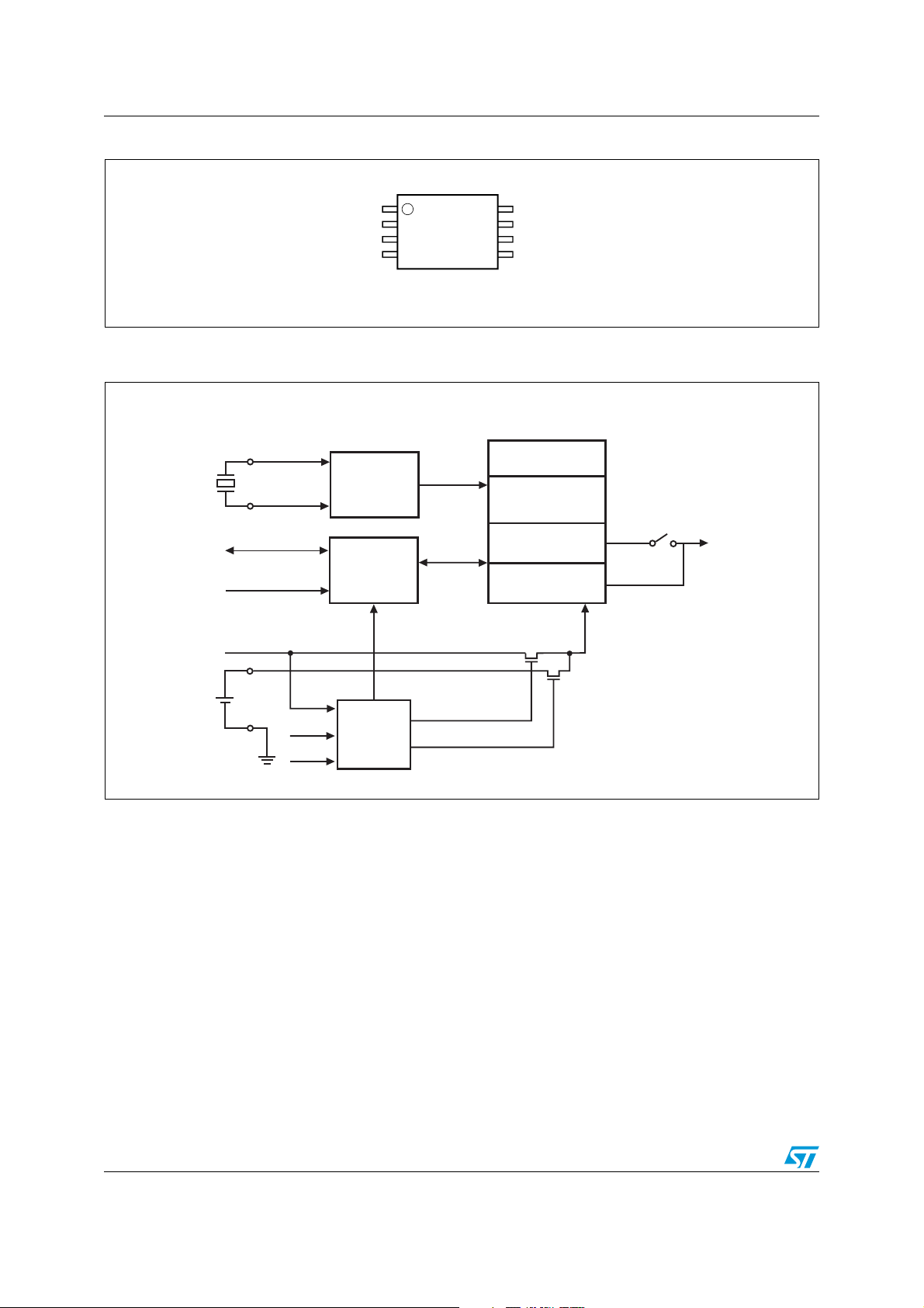
Figure 3. Block diagram
REAL TIME CLOCK
CALENDAR
OSCILLATOR FAIL
CIRCUIT
RTC &
CALIBRATION
CRYSTAL
32KHz
OSCILLATOR
SDA
SCL
V
CC
V
BAT
V
V
1. Open drain output
SO
PFD
I2C
INTERFACE
WRITE
PROTECT
COMPARE
FREQUENCY TEST
OUTPUT DRIVER
FT
OUT
INTERNAL
POWER
FT/OUT
AI09168
(1)
6/28 Doc ID 10772 Rev 5

M41T00S Operation
2 Operation
The M41T00S clock operates as a slave device on the serial bus. Access is obtained by
implementing a start condition followed by the correct slave address (D0h). The 8 bytes
contained in the device can then be accessed sequentially in the following order:
1. Seconds register
2. Minutes register
3. Century/hours register
4. Day register
5. Date register
6. Month register
7. Year register
8. Calibration register
The M41T00S clock continually monitors V
fall below V
, the device terminates an access in progress and resets the device address
PFD
counter. Inputs to the device will not be recognized at this time to prevent erroneous data
from being written to the device from a an out-of-tolerance system. Once V
switchover voltage (V
), the device automatically switches over to the battery and powers
SO
down into an ultra-low current mode of operation to preserve battery life. If V
V
, the device power is switched from VCC to V
PFD
greater than V
V
. Upon power-up, the device switches from battery to VCC at VSO. When VCC rises
PFD
above V
PFD
, the device power is switched from VCC to V
PFD
, it will recognize the inputs.
For more information on battery storage life refer to application note AN1012.
2.1 2-wire bus characteristics
The bus is intended for communication between different ICs. It consists of two lines: a
bidirectional data signal (SDA) and a clock signal (SCL). Both the SDA and SCL lines must
be connected to a positive supply voltage via a pull-up resistor.
The following protocol has been defined:
● Data transfer may be initiated only when the bus is not busy.
● During data transfer, the data line must remain stable whenever the clock line is high.
● Changes in the data line, while the clock line is high, will be interpreted as control
signals.
for an out-of-tolerance condition. Should VCC
CC
falls below the
CC
is less than
when VCC drops below V
BAT
when VCC drops below
BAT
BAT
BAT
. If V
BAT
is
Accordingly, the following bus conditions have been defined:
2.1.1 Bus not busy
Both data and clock lines remain high.
2.1.2 Start data transfer
A change in the state of the data line, from high to low, while the clock is high, defines the
START condition.
Doc ID 10772 Rev 5 7/28

Operation M41T00S
2.1.3 Stop data transfer
A change in the state of the data line, from low to high, while the clock is high, defines the
STOP condition.
2.1.4 Data valid
The state of the data line represents valid data when after a start condition, the data line is
stable for the duration of the high period of the clock signal. The data on the line may be
changed during the low period of the clock signal. There is one clock pulse per bit of data.
Each data transfer is initiated with a start condition and terminated with a stop condition.
The number of data bytes transferred between the start and stop conditions is not limited.
The information is transmitted byte-wide and each receiver acknowledges with a ninth bit.
By definition a device that gives out a message is called “transmitter,” the receiving device
that gets the message is called “receiver.” The device that controls the message is called
“master.” The devices that are controlled by the master are called “slaves.”
2.1.5 Acknowledge
Each byte of eight bits is followed by one acknowledge bit. this acknowledge bit is a low level
put on the bus by the receiver whereas the master generates an extra acknowledge related
clock pulse. A slave receiver which is addressed is obliged to generate an acknowledge
after the reception of each byte that has been clocked out of the slave transmitter.
The device that acknowledges has to pull down the SDA line during the acknowledge clock
pulse in such a way that the SDA line is a stable low during the high period of the
acknowledge related clock pulse. Of course, setup and hold times must be taken into
account. A master receiver must signal an end of data to the slave transmitter by not
generating an acknowledge on the last byte that has been clocked out of the slave. In this
case the transmitter must leave the data line high to enable the master to generate the
STOP condition.
Figure 4. Serial bus data transfer sequence
DATA LINE
STABLE
DATA VALID
CLOCK
DATA
START
CONDITION
CHANGE OF
DATA ALLOWED
STOP
CONDITION
AI00587
8/28 Doc ID 10772 Rev 5

M41T00S Operation
Figure 5. Acknowledgement sequence
CLOCK PULSE FOR
ACKNOWLEDGEMENT
SCL FROM
MASTER
START
12 89
DATA OUTPUT
BY TRANSMITTER
DATA OUTPUT
BY RECEIVER
2.2 READ mode
In this mode the master reads the M41T00S slave after setting the slave address (see
Figure 7 on page 10). Following the WRITE mode control bit (R/W
bit, the word address 'An' is written to the on-chip address pointer. Next the START condition
and slave address are repeated followed by the READ mode control bit (R/W
point the master transmitter becomes the master receiver. The data byte which was
addressed will be transmitted and the master receiver will send an acknowledge bit to the
slave transmitter. The address pointer is only incremented on reception of an acknowledge
clock. The M41T00S slave transmitter will now place the data byte at address An+1 on the
bus, the master receiver reads and acknowledges the new byte and the address pointer is
incremented to “An+2.”
This cycle of reading consecutive addresses will continue until the master receiver sends a
STOP condition to the slave transmitter.
The system-to-user transfer of clock data will be halted whenever the address being read is
a clock address (00h to 06h). The update will resume due to a stop condition or when the
pointer increments to any non-clock address (07h).
MSB LSB
AI00601
=0) and the acknowledge
=1). At this
Note: This is true both in READ mode and WRITE mode.
An alternate READ mode may also be implemented whereby the master reads the
M41T00S slave without first writing to the (volatile) address pointer. The first address that is
read is the last one stored in the pointer (see Figure 8 on page 10).
Figure 6. Slave address location
START A
SLAVE ADDRESS
MSB
0100011
Doc ID 10772 Rev 5 9/28
R/W
LSB
AI00602
 Loading...