


MCX18N00A/MCX18N00B
Micro Unit CCD
Description
The micro unit CCD is a CCD color camera unit with built-in CCD image sensor, drive system IC, sample-and-hold IC, signal processor IC and lens system.
Features
• Ultra-compact size:
MCX18N00A |
18.3mm × 18.3mm × 8.4mm |
MCX18N00B |
18.3mm × 18.3mm × 9.6mm |
•Y/C analog output
•Employs a Type 1/5,
180,000-pixel color CCD image sensor
•Equipped with a fixed focus lens:
MCX18N00A |
F2.8/f = 2.9mm |
MCX18N00B |
F2.8/f = 4.0mm |
Applications
•TV conference cameras
•Image input cameras
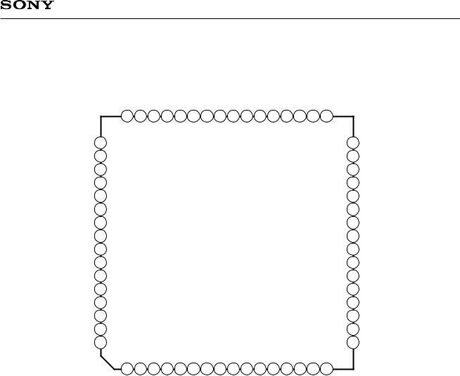
64 pin QFN (Ceramic)
Peripheral ICs
•EVR: MB88347 (Fujitsu Limited.)
•EEPROM: AK6420 (Asahi Kasei Microsystems
Co., Ltd.)
Absolute Maximum Ratings |
|
|
|
|
|
|
|
||||||
• Supply voltage |
VH |
|
+18 |
|
|
V |
|||||||
|
|
DVDD1, DVDD2, AVDD6 |
|
+7.0 |
|
|
V |
||||||
|
|
AVDD1, AVDD2, AVDD3 |
|
+7.0 |
|
|
V |
||||||
|
|
AVDD4, AVDD5 |
|
+7.0 |
|
|
V |
||||||
|
|
VCC |
|
+14.0 |
|
|
V |
||||||
• Input voltage |
VL |
|
|
–17.5 |
V |
||||||||
VI |
–0.5 to DVDD + 0.5 |
V |
|||||||||||
• Operating temperature |
Topr |
|
|
0 to +40 |
°C |
||||||||
• Storage temperature |
Tstg |
|
|
–30 to +80 |
°C |
||||||||
Recommended Operating Conditions |
|
|
|
|
|
|
|
||||||
• Supply voltage |
VH |
|
14.25 to 15.75 |
V |
|||||||||
|
|
DVDD1, DVDD2, AVDD6 |
|
|
3.0 to 3.6 |
V |
|||||||
|
|
AVDD1, AVDD2, AVDD3 |
|
4.75 to 5.25 |
V |
||||||||
|
|
AVDD4, AVDD5 |
|
|
4.5 to 5.5 |
V |
|||||||
|
|
VCC |
|
|
4.5 to 5.25 |
V |
|||||||
• Input voltage |
VL |
|
–8.5 to –7.5 |
V |
|||||||||
VDCIN |
|
|
1.0 to 4.5 |
V |
|||||||||
• Operating temperature |
Topr |
|
|
0 to +40 |
°C |
||||||||
Block Diagram |
|
|
|
|
|
|
|
|
|
|
|
|
|
|
|
|
|
|
|
|
|
|
|
||||
|
|
Lens |
|
|
|
|
|
|
|
||||
|
|
|
CCD |
|
|
|
|
|
Digital |
|
|
||
|
|
|
|
|
|
|
|
||||||
|
|
|
Image |
|
|
S/H |
|
|
Signal |
|
Y/C |
||
|
|
|
|
|
|||||||||
|
|
|
Sensor |
|
|
|
|
|
Process |
|
|
||
|
|
|
|
|
|
|
|
|
|
|
|
|
|
|
|
|
|
|
|
|
|
|
|
|
|
|
|
|
|
|
|
|
|
Timing |
|
|
|
|
|
|
|
|
|
|
|
|
|
Generator |
|
|
|
|
|||
|
|
|
|
|
|
|
|
|
|
|
|
|
|
|
|
|
|
|
|
|
|
|
|
|
|
|
|
Sony reserves the right to change products and specifications without prior notice. This information does not convey any license by any implication or otherwise under any patents or other right. Application circuits shown, if any, are typical examples illustrating the operation of the devices. Sony cannot assume responsibility for any problems arising out of the use of these circuits.
– 1 –
E97432B9X
MCX18N00A/MCX18N00B
Pin Configuration
CFE RI |
CFE RV |
CBV |
TUO DCC |
DNG D |
DNG D |
DNG D |
DH |
DV |
PMO CP |
DNG A |
OCS F4 |
ICS F4 |
6D
VD A
RLC X |
KCS |
56 55 54 53 52 51 50 49 48 47 46 45 44 43 42 41
VGC 57
AVDD5 58
IOC 59
IOY 60
VGY 61
IREFY 62
VREFY 63
VBY 64
DGND 1
DGND 2
DGND 3
SHOUT 4
SHIN 5
AGND 6
AGND 7
SIFSEL 8
9 10 11 12 13 14 15 16
DV2DD |
DNG A |
HV |
DNG A |
4VADD |
VCC |
TSE T |
NIBU S |
40 |
SI |
39 |
SO |
38 |
CASI |
37 |
CSROM |
36 |
RESETTG |
35 |
DGND |
34 |
OSCI |
33 |
OSCO |
32 |
CK |
31 |
DVDD1 |
30 |
XCS |
29 |
CASCK |
28 |
CASO |
27 |
CSEVR |
26 |
DGND |
25 |
VL |
17 18 19 20 21 22 23 24
TNO CCG A |
TES FFO |
1AVDD |
2AVDD |
AV3DD |
NICD |
TUO CD |
TUO BUS |
– 2 –

MCX18N00A/MCX18N00B
Pin Description
Pin |
Symbol |
I/O |
Description |
|
No. |
||||
|
|
|
||
|
|
|
|
|
1 |
DGND |
— |
Digital GND |
|
|
|
|
|
|
2 |
DGND |
— |
Digital GND |
|
|
|
|
|
|
3 |
DGND |
— |
Digital GND |
|
|
|
|
|
|
4 |
SHOUT |
O |
Sample-and-hold output. Connect directly to Pin 5. |
|
|
|
|
|
|
5 |
SHIN |
I |
Sample-and-hold input. |
|
|
|
|
|
|
6 |
AGND |
— |
Analog GND |
|
|
|
|
|
|
7 |
AGND |
I |
Analog GND |
|
|
|
|
|
|
8 |
SIFSEL |
I |
Serial communication mode selection: Microcomputer (low)/RS232C (high). |
|
|
|
|
|
|
9 |
DVDD2 |
— |
+3.3V power supply for signal processing system. |
|
|
|
|
|
|
10 |
AGND |
— |
Analog GND |
|
|
|
|
|
|
11 |
VH |
— |
+15V power supply for CCD image sensor drive. |
|
|
|
|
|
|
12 |
AGND |
— |
Analog GND |
|
|
|
|
|
|
13 |
AVDD4 |
— |
+5V power supply for A/D converter. |
|
|
|
|
|
|
14 |
VCC |
— |
+5V power supply for sample-and-hold. |
|
|
|
|
|
|
15 |
TEST |
I |
Test pin. Connect to VCC. |
|
|
|
|
|
|
16 |
SUBIN |
I |
CCD image sensor SUB voltage input. |
|
|
|
|
|
|
17 |
AGCCONT |
I |
AGC control. |
|
|
|
|
|
|
18 |
OFFSET |
I |
OFFSET control. |
|
|
|
|
|
|
19 |
AVDD1 |
— |
+5V power supply for sample-and-hold pulse. |
|
|
|
|
|
|
20 |
AVDD2 |
— |
+5V power supply for RG pulse. |
|
|
|
|
|
|
21 |
AVDD3 |
— |
+5V power supply for H pulse. |
|
|
|
|
|
|
22 |
DCIN |
I |
DC amplifier input. |
|
|
|
|
|
|
23 |
DCOUT |
O |
DC amplifier output. |
|
|
|
|
|
|
24 |
SUBOUT |
O |
SUB pulse output. |
|
|
|
|
|
|
25 |
VL |
— |
–8V power supply for CCD image sensor drive. |
|
|
|
|
|
|
26 |
DGND |
— |
Digital GND |
|
|
|
|
|
|
27 |
CSEVR |
O |
EVR chip select. |
|
|
|
|
|
|
28 |
CASO |
O |
Serial communication data output for peripheral ICs (EVR, EEPROM). |
|
|
|
|
|
|
29 |
CASCK |
O |
Serial communication clock output for peripheral ICs (EVR, EEPROM). |
|
|
|
|
|
|
|
|
|
Switched by the SIFSEL setting. |
|
30 |
XCS |
I |
Chip select during microcomputer mode. |
|
|
|
|
Baud rate setting (4800bps (low)/9600bps (high)) during RS232C mode. |
|
|
|
|
|
|
31 |
DVDD1 |
— |
+3.3V power supply for timing generator. |
|
|
|
|
|
|
32 |
CK |
I |
27MHz clock input. |
|
|
|
|
|
|
33 |
OSCO |
O |
27MHz oscillator output. |
|
|
|
|
|
|
34 |
OSCI |
I |
27MHz oscillator input. |
|
|
|
|
|
|
35 |
DGND |
— |
Digital GND |
|
|
|
|
|
|
|
|
|
– 3 – |

|
|
|
MCX18N00A/MCX18N00B |
|
|
|
|
|
|
|
|
|
|
|
Pin |
Symbol |
I/O |
Description |
|
No. |
||||
|
|
|
||
|
|
|
|
|
36 |
RESETTG |
I |
Reset pin (active low) with pull-up resistor for timing generator. |
|
|
|
|
|
|
37 |
CSROM |
O |
EEPROM chip select. |
|
|
|
|
|
|
38 |
CASI |
I |
Serial communication data input for peripheral ICs (EVR, EEPROM). |
|
|
|
|
|
|
39 |
SO |
O |
Serial communication data output. |
|
|
|
|
|
|
40 |
SI |
I |
Serial communication data input. |
|
|
|
|
|
|
41 |
SCK |
I |
Serial communication clock input. |
|
|
|
|
|
|
42 |
XCLR |
I |
Initialization pin (active low). EEPROM re-read. |
|
|
|
|
|
|
43 |
AVDD6 |
— |
+3.3V power supply for 4fsc oscillator. |
|
|
|
|
|
|
44 |
4FSCI |
I |
4fsc oscillator input. |
|
|
|
|
|
|
45 |
4FSCO |
O |
4fsc oscillator output. |
|
|
|
|
|
|
46 |
AGND |
— |
Analog GND |
|
|
|
|
|
|
47 |
PCOMP |
O |
Phase comparison output for PLL lock. |
|
|
|
|
|
|
48 |
VD |
O |
Vertical sync output. |
|
|
|
|
|
|
49 |
HD |
O |
Horizontal sync output. |
|
|
|
|
|
|
50 |
DGND |
— |
Digital GND |
|
|
|
|
|
|
51 |
DGND |
— |
Digital GND |
|
|
|
|
|
|
52 |
DGND |
— |
Digital GND |
|
|
|
|
|
|
53 |
CCDOUT |
O |
CCD image sensor buffer output. |
|
|
|
|
|
|
54 |
VBC |
|
|
|
|
|
|
|
|
55 |
VREFC |
I |
D/A converter peripheral circuit connection pins for chroma signal. |
|
|
|
|
||
56 |
IREFC |
|
||
|
|
|||
|
|
|
|
|
57 |
VGC |
|
|
|
|
|
|
|
|
58 |
AVDD5 |
— |
+5V power supply for D/A converter. |
|
|
|
|
|
|
59 |
IOC |
O |
Chroma signal output. |
|
|
|
|
|
|
60 |
IOY |
O |
Luminance signal output. |
|
|
|
|
|
|
61 |
VGY |
|
|
|
|
|
|
|
|
62 |
IREFY |
|
D/A converter peripheral circuit connection pins for luminance signal. |
|
|
|
|
||
63 |
VREFY |
I |
||
|
||||
|
|
|
|
|
64 |
VBY |
|
|
|
|
|
|
|
– 4 –

MCX18N00A/MCX18N00B
Electrical Characteristics
DC Characteristics
Item |
Pins |
Symbol |
Conditions |
Min. |
Typ. |
Max. |
|
Unit |
|
|
|
|
|
|
|
|
|
|
|
|
|
|
DVDD1 |
|
3.0 |
3.3 |
3.6 |
|
V |
|
|
|
|
|
|
|
|
|
|
|
|
|
DVDD2 |
|
3.0 |
3.3 |
3.6 |
|
V |
|
|
|
|
|
|
|
|
|
|
|
|
|
AVDD1 |
|
4.75 |
5.00 |
5.25 |
|
V |
|
|
|
|
|
|
|
|
|
|
|
|
|
AVDD2 |
|
4.75 |
5.00 |
5.25 |
|
V |
|
|
|
|
|
|
|
|
|
|
|
|
|
AVDD3 |
|
4.75 |
5.00 |
5.25 |
|
V |
|
|
|
|
|
|
|
|
|
|
Supply voltage |
|
AVDD4 |
A/D input amplitude = 2Vp-p |
4.5 |
5.0 |
5.5 |
|
V |
|
|
|
|
|
|
|
|
|
|
|
|
|
|
AVDD5 |
D/A output amplitude = 2Vp-p |
4.5 |
5.0 |
5.5 |
|
V |
|
|
|
|
|
|
|
|
|
|
|
|
|
AVDD6 |
|
3.0 |
3.3 |
3.6 |
|
V |
|
|
|
|
|
|
|
|
|
|
|
|
|
VCC |
|
4.5 |
5.0 |
5.25 |
|
V |
|
|
|
|
|
|
|
|
|
|
|
|
|
VH |
|
14.25 |
15.00 |
15.75 |
V |
|
|
|
|
|
|
|
|
|
|
|
|
|
|
VL |
|
–8.5 |
–8.0 |
–7.5 |
|
V |
|
|
|
|
|
|
|
|
|
|
|
|
|
IDD1 |
DVDD1 = 3.3V |
|
7.2 |
|
|
mA |
|
|
|
|
|
|
|
|
|
|
|
|
|
IDD2 |
DVDD2 = 3.3V |
|
36 |
|
|
mA |
|
|
|
|
|
|
|
|
|
|
|
|
|
IADD1 |
AVDD1 = 5.0V |
|
3.1 |
|
|
mA |
|
|
|
|
|
|
|
|
|
|
|
|
|
IADD2 |
AVDD2 = 5.0V |
|
1.0 |
|
|
mA |
|
|
|
|
|
|
|
|
|
|
Operating |
|
IADD3 |
AVDD3 = 5.0V |
|
4.9 |
|
|
mA |
|
|
|
|
|
|
|
|
|
||
|
IADD4 |
AVDD4 = 5.0V |
|
15 |
|
|
mA |
||
current |
|
|
|
|
|||||
|
|
|
|
|
|
|
|
||
|
|
|
IADD5 |
AVDD5 = 5.0V |
|
24 |
|
|
mA |
|
|
|
|
|
|
|
|
|
|
|
|
|
IADD6 |
AVDD6 = 3.3V |
|
1.0 |
|
|
mA |
|
|
|
|
|
|
|
|
|
|
|
|
|
ICC |
VCC = 5.0V |
|
54 |
|
|
mA |
|
|
|
|
|
|
|
|
|
|
|
|
|
IH |
VH = 15.0V |
|
6.9 |
|
|
mA |
|
|
|
|
|
|
|
|
|
|
|
|
|
IL |
VL = –8.0V |
|
1.4 |
|
|
mA |
|
|
|
|
|
|
|
|
|
|
Input voltage 1 |
5, 7 |
VT+ |
|
DVDD2 × 0.8 |
|
DVDD2 × |
0.2 |
V |
|
VT– |
|
|
|
||||||
|
|
|
|
|
|
|
|||
|
|
|
|
|
|
|
|
|
|
Input voltage 2 |
1, 6 |
VIH1 |
|
DVDD1 × 0.7 |
|
DVDD1 × |
0.3 |
V |
|
VIL1 |
|
|
|
||||||
|
|
|
|
|
|
|
|||
|
|
|
|
|
|
|
|
|
|
Input voltage 3 |
DCIN |
VDCIN |
|
1.0 |
|
4.5 |
|
V |
|
|
|
|
|
|
|
|
|
|
|
Input voltage 4 |
SUBIN |
VSUB |
|
Display |
Display |
Display |
|
V |
|
|
value – 0.1 |
value |
value + 0.1 |
||||||
|
|
|
|
|
|
||||
|
|
|
|
|
|
|
|
|
|
Input voltage 5 |
4FSCI |
VIH2 |
|
AVDD4 × 0.7 |
|
|
|
V |
|
VIL2 |
|
|
|
DD |
0.3 |
||||
|
|
|
|
|
|
|
AV 4 × |
|
|
– 5 –

MCX18N00A/MCX18N00B
|
Item |
Pins |
Symbol |
Conditions |
Min. |
Typ. |
Max. |
Unit |
|
|
|
|
|
|
|
|
|
Output voltage 1 |
2 |
VOH1 |
IOH1 = –1.2mA |
DVDD2 – 0.8 |
|
0.4 |
V |
|
|
VOL1 |
IOL1 = 2.4mA |
|
|
||||
|
|
|
|
|
|
|||
|
|
|
|
|
|
|
|
|
Output voltage 2 |
3 |
VOH2 |
IOH2 = –2.4mA |
DVDD2 – 0.8 |
|
0.4 |
V |
|
|
VOL2 |
IOL2 = 4.8mA |
|
|
||||
|
|
|
|
|
|
|||
|
|
|
|
|
|
|
|
|
Output voltage 3 |
4 |
VOH3 |
IOH3 = –8mA |
DVDD1/2 |
|
DVDD1/2 |
V |
|
|
VOL3 |
IOL3 = 8mA |
|
|
||||
|
|
|
|
|
|
|||
|
|
|
|
|
|
|
|
|
Output voltage 4 |
SUBOUT |
VOH4 |
IOH4 = –4mA |
VH – 0.25 |
|
VL + 0.25 |
V |
|
VOL4 |
IOL4 = 5.4mA |
|
|
|||||
|
|
|
|
|
|
|
|
|
Output voltage 5 |
4FSCO |
VOH5 |
IOH5 = –3mA |
AVDD4/2 |
|
AVDD4/2 |
V |
|
VOL5 |
IOL5 = 3mA |
|
|
|||||
|
|
|
|
|
|
|||
|
|
|
|
|
|
|
|
|
Hysteresis 1 |
7 |
|
|
|
0.5 |
|
V |
|
|
|
|
|
|
||||
|
|
|
|
|
|
|
|
|
Hysteresis 2 |
5 |
|
|
|
0.6 |
|
V |
|
|
|
|
|
|
|
|
|
|
Threshold value 1 |
TEST |
VTH1 |
|
|
1.35 |
|
V |
|
|
|
|
|
|
|
|
|
|
Threshold value 2 |
6 |
VTH2 |
|
|
DVDD1/2 |
|
V |
|
|
|
|
|
|||||
|
|
|
|
|
|
|
|
|
Threshold value 3 |
4FSCI |
VTH3 |
|
|
AVDD4/2 |
|
V |
|
|
|
|
|
|
|
|
|
|
Feedback resistance 1 |
OSC |
RFE1 |
OSCI = DVDD1 or GND |
500k |
2M |
5M |
Ω |
|
|
|
|
|
|
|
|
|
|
Feedback resistance 2 |
4FSC |
RFE2 |
4FSCI = AVDD4 or GND |
250k |
1M |
2.5M |
Ω |
|
|
|
|
|
|
|
|
|
|
Input amplitude |
OSC |
|
50MHz sine wave |
0.5 |
|
|
Vp-p |
|
|
|
|
|
|
|
|
|
|
Pull-up resistance |
1 |
RPU |
|
50k |
100k |
150k |
Ω |
|
|
|
|
|
|
|
|
|
|
DC amplifier gain |
|
G |
|
|
4.4 |
|
|
|
|
|
|
|
|
|
|
|
|
Input leak current 1 |
SIFSEL |
II3 |
VIN = DVDD2 |
12 |
30 |
75 |
µA |
|
|
|
|
|
|
|
|
|
|
Input leak current 2 |
5 |
II2 |
VIN = GND or DVDD2 |
–10 |
|
10 |
µA |
|
|
|
|
|
|
|
|
|
|
1 |
RESETTG |
|
|
|
|
|
|
|
2 |
CSEVR, CSROM, SO, PCOMP, VD, HD |
|
|
|
|
|||
3 |
CASO, CASCK |
|
|
|
|
|
|
|
4 |
OSCO |
|
|
|
|
|
|
|
5 |
XCS, SI, SCK, XCLR, CASI |
|
|
|
|
|
|
|
6 |
OSCI, CK |
|
|
|
|
|
|
|
7 |
SIFSEL |
|
|
|
|
|
|
|
– 6 –
 Loading...