


LCX019AM
3.4cm (1.32-inch) LCD Panel (with microlens)
For the availability of this product, please contact the sales office.
Description
The LCX019AM is a 3.4cm diagonal active matrix TFT-LCD panel addressed by polycrystalline silicon super thin film transistors with built-in peripheral driving circuit. This panel allows full-color representation without color filters through the use of a microlens.
This panel has an aspect ratio of 4:3 and supports
NTSC/PAL display.
This panel has a polysilicon TFT high-speed scanner and built-in function to display images up/down and/or right/left inverse. The built-in 5V interface circuit leads to lower voltage of timing and control signals.
Features
•The number of active dots: 576,000 (1.32-inch; 3.4cm in diagonal)
•Horizontal resolution: 600TV lines
•Effective aperture ratio: 70% (reference value)
•High contrast ratio with normally white mode: 200 (typ.)
•Built-in H and V drivers (built-in input level conversion circuit, 5V driving possible)
•Supports NTSC
(PAL mode also available through conversion of scanned dot numbers by an external IC)
•Up/down and/or right/left inverse display function
Element Structure
•Dots: 1199.5 (H) × 480 (V) = 575,760
•Built-in peripheral driver using polycrystalline silicon super thin film transistors.
Applications
Liquid crystal projectors, etc.
Sony reserves the right to change products and specifications without prior notice. This information does not convey any license by any implication or otherwise under any patents or other right. Application circuits shown, if any, are typical examples illustrating the operation of the devices. Sony cannot assume responsibility for any problems arising out of the use of these circuits.
– 1 –
E97106A94-PS

LCX019AM
Block Diagram
GIS P |
TSH |
1KC H |
2KC .C H .N |
TGR |
TSV |
KCV |
GCP |
NW D |
BNE |
AVDD |
HVDD |
VVDD |
VSS |
VGSS |
)2B (6G IS |
)2R (5G IS |
)2G (4G IS |
)1B (3G IS |
)1R (2G IS |
)1G (1G IS |
MOC |
3 |
14 |
15 |
16 12 |
13 |
20 |
19 |
22 |
21 |
18 |
10 |
11 |
23 |
17 |
2 |
9 |
8 |
7 |
6 |
5 |
4 |
1 |
rell ortn oC |
|
|
Level |
|
|
|
|
|
|
Bi-directional H Driver |
|
|
|
|
|
|
|
||||
|
|
Shifter |
|
|
|
|
|
|
|
|
|
|
|
|
|
||||||
|
|
|
|
|
|
|
|
|
|
|
|
|
|
|
|
|
|
|
|
||
|
|
|
|
|
|
|
|
|
|
|
|
|
|
|
|
|
|
|
|
|
|
edo M |
|
|
|
|
|
|
|
|
|
|
|
|
|
|
|
|
|
|
|
|
|
|
|
rev irD |
|
|
|
|
|
|
|
|
|
|
|
|
|
|
|
|
|
|
rev irD |
|
|
Vla noit ceri d-iB |
|
|
|
|
|
|
|
|
|
|
|
|
|
|
|
|
|
|
Vla noit ceri d-iB |
|
|
|
|
|
|
|
|
|
|
|
|
|
|
|
|
|
|
|
VCOM |
|
|
|
|
|
egra rell h o cer rtno P C |
|
|
|
|
|
|
|
|
|
|
|
|
|
|
|
|
|
|
– 2 –

LCX019AM
Absolute Maximum Ratings (VSS = 0V) |
|
|
|
|
||||||
• H driver supply voltage |
|
HVDD |
|
–1.0 to +20 |
V |
|||||
• V driver supply voltage |
|
VVDD |
|
–1.0 to +20 |
V |
|||||
• Analog block drive supply voltage |
AVDD |
|
–1.0 to +20 |
V |
||||||
• Common pad voltage |
|
COM |
|
–1.0 to +17 |
V |
|||||
• H shift register input pin voltage |
HST, HCK1, HCK2 |
|
–1.0 to +17 |
V |
||||||
|
|
|
|
|
RGT |
|
|
|
|
|
• V shift register input pin voltage |
VST, VCK, PCG |
|
–1.0 to +17 |
V |
||||||
|
|
|
|
|
ENB, DWN |
|
|
|
|
|
• Video signal input pin voltage |
|
SIG1, SIG2, SIG3, SIG4 |
–1.0 to +15 |
V |
||||||
|
|
|
|
|
SIG5, SIG6, PSIG |
|
|
|
|
|
• Operating temperature |
|
Topr |
|
–10 to +70 |
°C |
|||||
• Storage temperature |
|
Tstg |
|
–30 to +85 |
°C |
|||||
Operating Conditions (VSS = 0V) |
|
|
|
|
|
|
||||
• Supply voltage |
|
|
|
|
|
|
|
|||
|
HVDD |
13.5 ± 0.3 |
V |
|
|
|
|
|
|
|
|
VVDD |
13.5 ± 0.3 |
V |
|
|
|
|
|
|
|
|
AVDD |
15.5 ± 0.3 |
V |
|
|
|
|
|
|
|
• Input pulse voltage (Vp-p of all input pins except video signal and side black signal input pins) |
||||||||||
|
Vin |
5.0 ± 0.5 |
V |
|
|
|
|
|
|
|
Pin Description |
|
|
|
|
|
|
|
|||
|
|
|
|
|
|
|
|
|
|
|
Pin |
Symbol |
|
Description |
|
Pin |
Symbol |
|
Description |
||
No. |
|
|
No. |
|
||||||
|
|
|
|
|
|
|
|
|
||
|
|
|
|
|
|
|
|
|
|
|
1 |
COM |
|
Common voltage of panel |
|
13 |
RGT |
Drive direction pulse for H shift |
|||
|
|
register (H: normal, L: reverse) |
||||||||
|
|
|
|
|
|
|
|
|
||
|
|
|
|
|
|
|
|
|
|
|
2 |
VSSG |
|
Analog block GND |
|
14 |
HST |
Start pulse for H shift register |
|||
|
|
drive |
|
|||||||
|
|
|
|
|
|
|
|
|
|
|
|
|
|
|
|
|
|
|
|
|
|
3 |
PSIG |
|
Improvement pulse for uniformity |
|
15 |
HCK1 |
Clock pulse for H shift register |
|||
|
|
drive |
|
|||||||
|
|
|
|
|
|
|
|
|
|
|
|
|
|
|
|
|
|
|
|
|
|
4 |
SIG1 (G1) |
Video signal 1 (G) to panel |
|
16 |
HCK2 |
Clock pulse for H shift register |
||||
|
drive |
|
||||||||
|
|
|
|
|
|
|
|
|
|
|
|
|
|
|
|
|
|
||||
5 |
SIG2 (R1) |
Video signal 2 (R) to panel |
|
17 |
VSS |
GND (H, V drivers) |
||||
|
|
|
|
|
|
|
||||
6 |
SIG3 (B1) |
Video signal 3 (B) to panel |
|
18 |
ENB |
Enable pulse for gate selection |
||||
|
|
|
|
|
|
|
|
|
|
|
7 |
SIG4 (G2) |
Video signal 4 (G) to panel |
|
19 |
VCK |
Clock pulse for V shift register |
||||
|
drive |
|
||||||||
|
|
|
|
|
|
|
|
|
|
|
|
|
|
|
|
|
|
|
|
|
|
8 |
SIG5 (R2) |
Video signal 5 (R) to panel |
|
20 |
VST |
Start pulse for V shift register |
||||
|
drive |
|
||||||||
|
|
|
|
|
|
|
|
|
|
|
|
|
|
|
|
|
|
|
|
|
|
9 |
SIG6 (B2) |
Video signal 6 (B) to panel |
|
21 |
DWN |
Drive direction pulse for V shift |
||||
|
register (H: normal, L: reverse) |
|||||||||
|
|
|
|
|
|
|
|
|
||
|
|
|
|
|
|
|
|
|
|
|
10 |
AVDD |
|
Analog block power supply |
|
22 |
PCG |
Improvement pulse (2) for |
|||
|
|
uniformity |
||||||||
|
|
|
|
|
|
|
|
|
||
|
|
|
|
|
|
|
|
|||
11 |
HVDD |
|
Power supply for H driver |
|
23 |
VVDD |
Power supply for V driver |
|||
|
|
|
|
|
|
|
|
|
|
|
12 |
N.C. |
|
|
|
|
|
24 |
TEST |
Test; Open |
|
|
|
|
|
|
|
|
|
|
|
|
|
|
|
|
|
– 3 – |
|
|
|
||
LCX019AM
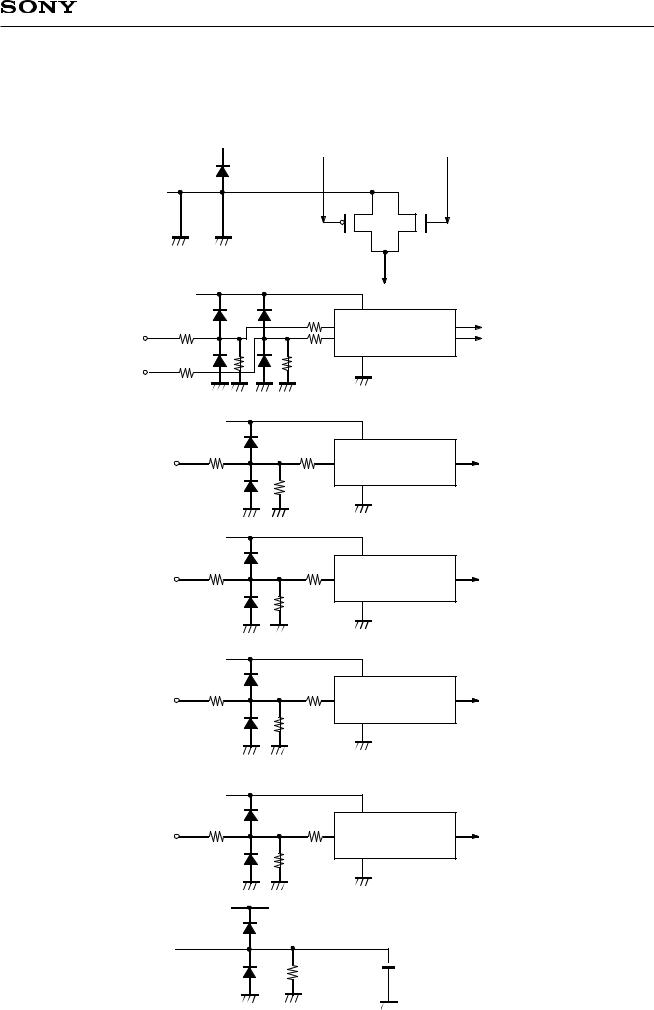
Input Equivalent Circuit
To prevent static charges, protective diodes are provided for each pin except the power supply. In addition, protective resistors are added to all pins except video signal input. All pins are connected to VSS with a high resistance of 1MΩ (typ.). The equivalent circuit of each input pin is shown below: (The resistor value: typ.)
(1) SIG1, SIG2, SIG3, SIG4, SIG5, SIG6, PSIG
HVDD 
Input 
 1MΩ
1MΩ 
|
VSS |
VSS |
|
(2) HCK1, HCK2 |
|
|
Signal line |
|
|
|
|
|
HVDD |
|
|
|
250Ω |
250Ω |
|
|
Level conversion circuit |
||
|
|
|
|
|
|
|
(2-phase input) |
Input |
250Ω |
250Ω |
|
|
1MΩ |
||
|
|
|
|
|
|
|
VSS |
|
|
1MΩ |
|
(3) RGT |
|
HVDD |
|
|
|
|
|
|
|
2.5kΩ |
2.5kΩ |
|
Input |
|
Level conversion circuit |
|
|
(single-phase input) |
|
|
|
|
|
|
|
|
1MΩ |
|
|
|
VSS |
(4) HST |
|
HVDD |
|
|
|
|
|
|
|
250Ω |
250Ω |
|
Input |
|
Level conversion circuit |
|
|
(single-phase input) |
|
|
|
|
|
|
|
|
1MΩ |
|
|
|
VSS |
(5) PCG, VCK |
|
|
|
|
|
VVDD |
|
|
|
250Ω |
250Ω |
|
Input |
|
Level conversion circuit |
|
|
(single-phase input) |
|
|
|
|
|
|
|
|
1MΩ |
|
|
|
VSS |
(6) VST, ENB, DWN |
|
|
|
|
|
VVDD |
|
|
|
2.5kΩ |
2.5kΩ |
|
Input |
|
Level conversion circuit |
|
|
(single-phase input) |
|
|
|
|
|
|
|
|
1MΩ |
|
|
|
VSS |
(7) COM |
|
VVDD |
|
|
|
|
|
Input 
 LC
LC
1MΩ
VSS
– 4 –
LCX019AM
Input Signals |
|
|
|
|
|
|
1. Input signal voltage conditions |
|
|
|
(Vss = 0V) |
||
|
|
|
|
|
|
|
Item |
|
Symbol |
Min. |
Typ. |
Max. |
Unit |
|
|
|
|
|
|
|
H driver input voltage |
(Low) |
VHIL |
–0.5 |
0.0 |
0.3 |
V |
RGT, HST, HCK1, HCK2 |
(High) |
VHIH |
4.5 |
5.0 |
5.5 |
V |
|
|
|
|
|
|
|
V driver input voltage |
(Low) |
VVIL |
–0.5 |
0.0 |
0.3 |
V |
ENB, VCK, PCG, VST, DWN |
(High) |
VVIH |
4.5 |
5.0 |
5.5 |
V |
|
|
|
|
|
|
|
Video signal center voltage |
|
VVC |
6.8 |
7.0 |
7.2 |
V |
|
|
|
|
|
|
|
Video signal input range 1 (SIG1 to 6) |
Vsig |
VVC – 4.5 |
— |
VVC + 4.5 |
V |
|
Common voltage of panel 2 |
|
Vcom |
VVC – 0.3 |
VVC – 0.2 |
VVC – 0.1 |
V |
Uniformity improvement signal input |
Vpsig |
VVC ± 3.4 |
VVC ± 3.5 |
VVC ± 3.6 |
V |
|
(PSIG) 3 |
|
|||||
|
|
|
|
|
||
123
Video input signal shall be symmetrical to VVC.
Common voltage of the panel shall be adjusted to VVC – 0.2 V.
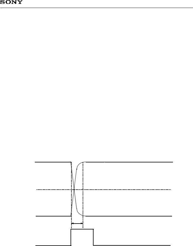
The uniformity improvement signal PSIG shall be input with the same polarity as video signals SIG1 to 6 and symmetrically with respect to VVC. Also, the PSIG rise and fall shall be synchronized with the PCG pulse rise and the time between the rise trPSIG and fall tfPSIG shall be kept to 800ns or less. (See the figure below.)
Uniformity Improvement Signal PSIG Input Waveform
90%
VVC
PSIG
10%
trPSIG
tfPSIG
PCG
Level Conversion Circuit
The LCX019AM has a built-in level conversion circuit in the clock input unit on the panel. The input signal level increases to HVDD or VVDD. The VCC of external ICs are applicable to 5 ± 0.5V.
– 5 –

|
|
|
|
|
|
LCX019AM |
|
|
|
|
|
|
|
|
|
2. Clock timing conditions |
(Ta = 25°C) (fHCKn = 3.82MHz, fVCK = 15.7kHz) |
||||||
|
|
|
|
|
|
|
|
|
Item |
Symbol |
Min. |
Typ. |
Max. |
|
Unit |
|
|
|
|
|
|
|
|
|
Hst rise time |
trHst |
— |
— |
30 |
|
|
|
|
|
|
|
|
|
|
HST |
Hst fall time |
tfHst |
— |
— |
30 |
|
|
|
|
|
|
|
|
|
|
Hst data set-up time |
tdHst |
–15 |
0 |
15 |
|
|
|
|
|
|
|||||
|
|
|
|
|
|
|
|
|
Hst data hold time |
thHst |
116 |
131 |
146 |
|
|
|
|
|
|
|
|
|
|
|
Hckn 4 rise time |
trHckn |
— |
— |
30 |
|
ns |
HCK |
Hckn 4 fall time |
tfHckn |
— |
— |
30 |
|
|
|
|
||||||
Hck1 fall to Hck2 rise time |
to1Hck |
–15 |
0 |
15 |
|
|
|
|
|
|
|||||
|
|
|
|
|
|
|
|
|
Hck1 rise to Hck2 fall time |
to2Hck |
–15 |
0 |
15 |
|
|
|
|
|
|
|
|
|
|
|
Vst rise time |
trVst |
— |
— |
100 |
|
|
|
|
|
|
|
|
|
|
VST |
Vst fall time |
tfVst |
— |
— |
100 |
|
|
|
|
|
|
|
|
|
|
Vst data set-up time |
tdVst |
5 |
15 |
25 |
|
µs |
|
|
|
||||||
|
|
|
|
|
|
|
|
|
Vst data hold time |
thVst |
5 |
15 |
25 |
|
|
|
|
|
|||||
|
|
|
|
|
|
|
|
VCK |
Vck rise time |
trVck |
— |
— |
100 |
|
|
|
|
|
|
|
|
|
|
Vck fall time |
tfVck |
— |
— |
100 |
|
|
|
|
|
|
|||||
|
|
|
|
|
|
|
|
|
Enb rise time |
trEnb |
— |
— |
100 |
|
|
|
|
|
|
|
|
|
|
ENB |
Enb fall time |
tfEnb |
— |
— |
100 |
|
|
|
|
|
|
|
|
|
|
Vck rise/fall to Enb rise time |
tdEnb |
350 |
400 |
450 |
|
ns |
|
|
|
||||||
|
|
|
|
|
|
|
|
|
Enb pulse width |
twEnb |
3450 |
3500 |
3550 |
|
|
|
|
|
|||||
|
|
|
|
|
|
|
|
|
Pcg rise time |
trPcg |
— |
— |
20 |
|
|
|
|
|
|
|
|
|
|
PCG |
Pcg fall time |
tfPcg |
— |
— |
20 |
|
|
|
|
|
|
|
|
|
|
Pcg fall to Vck rise/fall time |
toVck |
250 |
300 |
350 |
|
|
|
|
|
|
|||||
|
|
|
|
|
|
|
|
|
Pcg pulse width |
twPcg |
1750 |
1800 |
1850 |
|
|
|
|
|
|
|
|
|
|
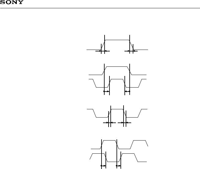
4 Hckn means Hck1 and Hck2. |
|
|
|
|
|
|
|
– 6 –
LCX019AM
<Horizontal Shift Register Driving Waveform>
|
Item |
Symbol |
|
|
|
Waveform |
Conditions |
||
|
|
|
|
|
|
|
|
|
|
|
Hst rise time |
trHst |
|
|
|
90% |
90% |
|
• Hckn 4 |
|
|
|
|
|
Hst |
10% |
10% |
|
duty cycle 50% |
|
|
|
|
|
|
to1Hck = 0ns |
|||
|
|
|
|
|
|
|
|
|
|
|
Hst fall time |
tfHst |
|
|
|
trHst |
tfHst |
|
to2Hck = 0ns |
|
|
|
|
|
|
|
|
||
|
|
|
|
|
|
|
|
|
|
|
|
|
|
|
|
|
|
|
|
HST |
|
|
|
|
5 |
|
|
|
|
Hst data set-up time |
tdHst |
|
|
|
50% |
50% |
|
|
|
|
|
|
Hst |
|
• Hckn 4 |
||||
|
|
|
|
|
|
|
|
|
|
|
|
|
|
|
Hck1 |
|
|
|
duty cycle 50% |
|
|
|
|
|
50% |
50% |
|
to1Hck = 0ns |
|
|
Hst data hold time |
thHst |
|
|
|
|
|
|
to2Hck = 0ns |
|
|
|
|
|
|
|
|
||
|
|
|
|
|
|
tdHst |
thHst |
|
|
|
|
|
|
|
|
|
|
|
|
|
|
|
|
|
|
|
|
|
|
|
|
|
|
|
|
|
|
|
|
|
Hckn 4 rise time |
trHckn |
|
|
4 |
90% |
90% |
|
• Hckn 4 |
|
|
|
10% |
10% |
|
||||
|
|
|
|
|
Hckn |
|
duty cycle 50% |
||
|
Hckn 4 fall time |
|
|
|
|
|
|
|
to1Hck = 0ns |
|
tfHckn |
|
|
|
trHckn |
tfHckn |
|
to2Hck = 0ns |
|
|
|
|
|
|
|
|
|
||
HCK |
|
|
|
|
|
|
|
|
|
|
|
|
|
|
|
|
|
|
|
|
|
|
|
|
|
|
|
|
|
Hck1 fall to Hck2 rise |
|
|
|
5 |
50% |
50% |
|
|
|
|
to1Hck |
|
|
Hck1 |
|
|
|||
|
time |
|
|
|
|
|
|
||
|
|
|
|
|
|
|
|
|
|
|
|
|
|
|
|
50% |
50% |
|
|
|
Hck1 rise to Hck2 fall |
|
|
|
|
|
|
||
|
to2Hck |
|
|
Hck2 |
|
|
|
|
|
|
time |
|
|
|
|
|
|
|
|
|
|
|
|
|
to2Hck to1Hck |
|
|
||
|
|
|
|
|
|
|
|
||
|
|
|
|
|
|
|
|
|
|
|
|
|
|
|
|
|
|
|
|
– 7 –
 Loading...