


CXA1163P
Sony CXA1163P, CXA1163M, CXA1102P, CXA1102M, CXA1101P Datasheet
...
– 1 –
CXA1100P, CXA1101P/M, CXA1102P/M, CXA1163P/M
E90302A13-PP
Dolby
∗
B Type Noise Reduction System
Description
CXA1100, CXA1101, CXA1102 and CXA1163 are
ICs including two separate Dolby B type noise
reduction processors. Seven devices with four Dolby
levels and two types of package are provided for
various applications. These devices feature very few
external components, which is achieved by
integrated filter circuits using integrated thin film
capacitors with high capacitance.
Features
• Minimum number of external components
• NR ON/OFF and REC/PB switchs included
• Small package (DIP16, SOP16)
• Small supply current (
~
—
5.5mA, Typ.)
• Dual channel processors in one chip
Absolute Maximum Ratings (Ta = 25°C)
• Supply voltage VCC 17 V
• Operating temperature Topr –30 to +85 °C
• Storage temperature Tstg –55 to +150 °C
• Allowable power dissipation PD
DIP16 (A1100P/A1101P/A1102P/A1163P)900 mW
SOP16 (A1101M/A1102M/A1163M) 500 mW
Note 1) These ICs are available only to the
licensees of Dolby Laboratories Licensing
Corporation from whom licensing and
application information may be obtaind.
Note 2) "Dolby" and double D symbols are trade
marks of Dolby Laboratories Licensing
Corporation.
Sony reserves the right to change products and specifications without prior notice. This information does not convey any license by
any implication or otherwise under any patents or other right. Application circuits shown, if any, are typical examples illustrating the
operation of the devices. Sony cannot assume responsibility for any problems arising out of the use of these circuits.
16 pin DIP (Plastic) 16 pin SOP (Plastic)
For the availability of this product, please contact the sales office.
– 2 –
CXA1100/CXA1101/CXA1102/CXA1163
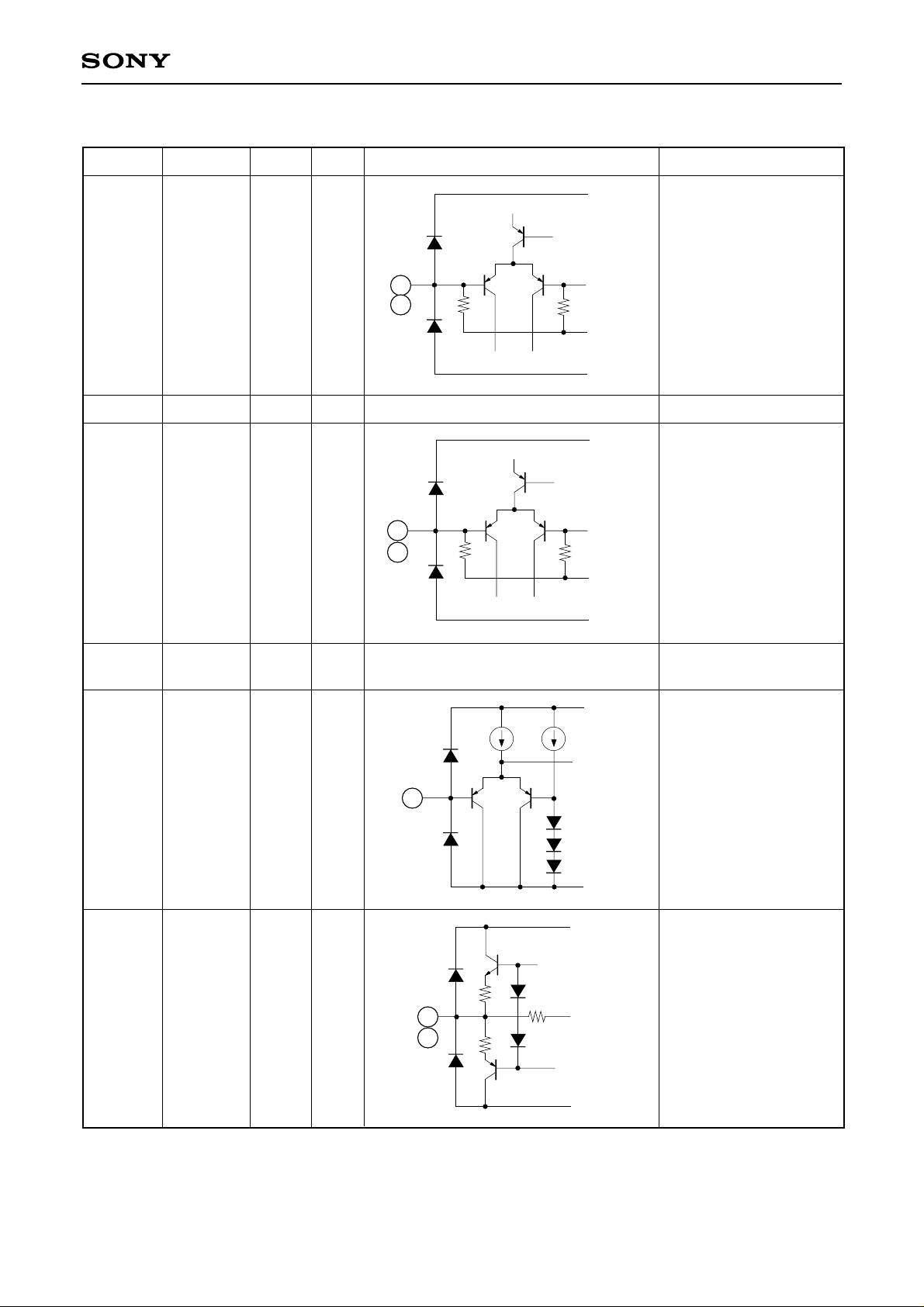
Pin Description (Ta = 25°C, VCC = 12V (Single supply), No signal)
No.
Symbol
Z (in)
VDC
Equivalent Circuit
Description
2
VCC
—
12.0V
Power supply
1, 16
REC IN
40kΩ
6.0V
Recording (Encode)
input
Vcc
GND
40k
Vcc/2
1
16
3, 14
PB IN
40kΩ
6.0V
Playback (Decode) input
Vcc
GND
40k
Vcc/2
14
3
5
ON/OFF
—
—
Mode control pin for NR
ON/OFF
"H" → NR OFF
"L" → NR ON
Vcc
GND
50µ
150µ
5
6, 11
LINE OUT
—
6.0V
Line (Decode) output
Vcc
GND
150
150
6
11
4
VCC/2
1kΩ
6.0V
Single supply → VCC/2
Split supply → Ground
– 3 –
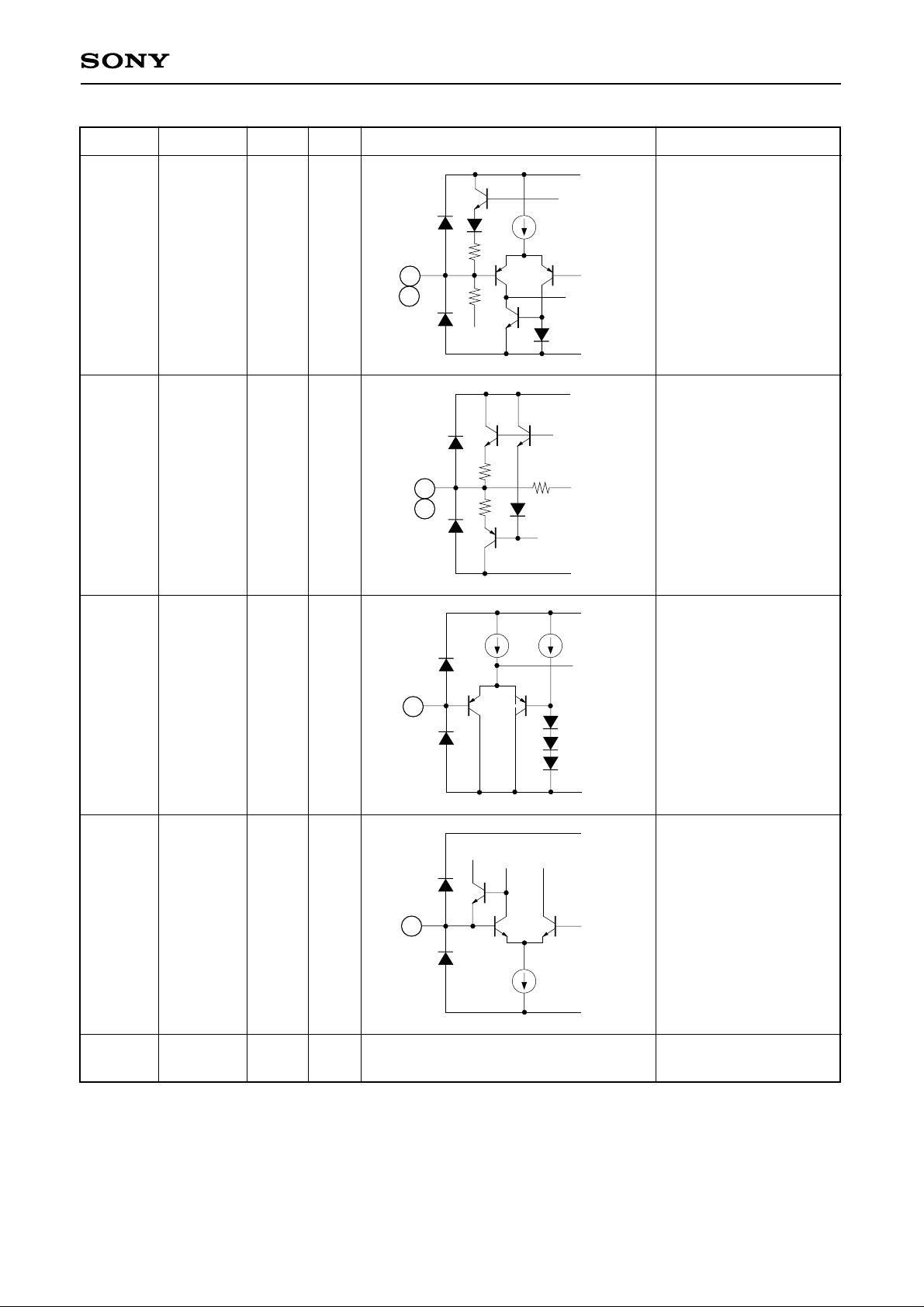
CXA1100/CXA1101/CXA1102/CXA1163
No.
Symbol
Z (in)
VDC
Equivalent Circuit
Description
7, 10
TC
—
0.3V
Time constant pin for
the level detector
Vcc
GND
4µ
8.2k
100k
7
10
8, 9
REC OUT
—
6.0V
Recording (Encode)
output
Vcc
GND
300
8.2k
300
8
9
12
REC/PB
—
—
Mode control pin for
REC/PB
(Encode/Decode)
"H" → B (Decode)
"L → EC (Encode)
Vcc
GND
50µ 150µ
12
13
IREF
—
1.2V
Reference current input
pin for the active filters
15
GND
—
0V
Single supply → Ground
Split supply → VEE
Vcc
GND
10µ
1.2V
13
– 4 –
CXA1100/CXA1101/CXA1102/CXA1163
Block Diagram
Test Circuit
C21
1µ
C22
1µ
C24
4.7µ
LINE OUT
C23
0.68µ
C14
4.7µ
LINE OUT
C13
0.68µ
R1
43k
C12
1µ
C11
1µ
PB IN
PB IN
REC IN
C1
100µ
REC IN
4
5
7
12
2
13
ATT2
ATT3
ATT3
SC DET
ATT2
ATT3
ATT1
SC DET
6
3
1
ATT2
ATT3
ATT1
SC DET
9
10
11
1415
16
8
Vcc
ON/OFF
REC OUT
C25
4.7µ
ATT: Attenuator
SC : Side Chain
DET: Detector
C15
4.7µ
REC OUT
REC/PB
R
P
R21
5.1k
OFF
S4
C21
1µ
R22
5.1k
C2
100µ
C22
1µ
C1
100µ
R5
510
S2
P
R
S1
C24
4.7µ
P
R
S5-2
C23
0.68µ
R
P
R11
5.1k
OFF
S3
C11
1µ
R12
5.1k
C12
1µ
R1
43k
C14
4.7µ
P
R
S5-1
C13
0.68µ
3
4
5
6
7
8
9
10
11
12
1415
1
2
13
16
R3
12k
Audio
SG
A
Vcc
+15V
1
2
S6-2
R2
10k
DC Level
Meter
C25
4.7µ
1
2
S6-1
CCIR/ARM
Filter
OFF
ON
S7
AC Level
Meter
Distortion
Analyzer
ON
OFF
R4
2k
C16
4.7µ
– 5 –
CXA1100/CXA1101/CXA1102/CXA1163
Electrical Characteristics Ta = 25°C, Dolby Level: –10dBm ( = 245mVrms) at REC OUT
VCC = 15V (CXA1100), VCC = 12V (CXA1101), VCC = 9V (CXA1102)
VCC = 6V (CXA1163)
Item Symbol
R/P NR f (Hz) Other Conditions
Test Condition
∗
Min. Typ. Max. Unit
Operating voltage
CXA1100
CXA1101
CXA1102
CXA1163
Supply current
CXA1100
CXA1101
CXA1102
CXA1163
LINE OUT level
CXA1100
CXA1101
CXA1102
CXA1163
REC IN level
PB IN level
Encode characteristics
(Boost)
(1)
(2)
(3)
(4)
(5)
Signal handling
CXA1100
CXA1101
CXA1102
CXA1163
Vopr
ICC
Vlout
Vrin
Vpin
B-R-1
B-R-2
B-R-3
B-R-4
B-R-5
Vomax
—
R
R
R
P
R
R
R
R
R
R
—
OFF
OFF
OFF
OFF
ON
ON
ON
ON
ON
OFF
—
—
1k
1k
1k
500
2k
5k
10k
10k
1k
Signal Handling
≥ 12dB
No signal
–25dB
–25dB
–25dB
–40dB
0dB
THD = 1%
11.5
8.5
6.5
5.0
3.5
3.5
3.5
3.5
–1.0
–4.0
–7.0
–11.0
–32
–32
1.4
5.5
3.9
9.7
–1.1
13.5
14.0
14.0
13.0
—
—
—
—
5.6
5.5
5.3
5.1
0.0
–3.0
–6.0
–10.0
–30
–30
2.9
7.0
5.4
10.4
0.4
15.3
15.9
15.9
15.0
16.0
16.0
16.0
16.0
7.5
7.5
7.5
7.5
1.0
–2.0
–5.0
–9.0
–28
–28
4.4
8.5
6.9
11.9
1.9
—
—
—
—
V
V
V
V
mA
mA
mA
mA
dBm
dBm
dBm
dBm
dBm
dBm
dB
dB
dB
dB
dB
dB
dB
dB
dB
0dBm = 0.775Vrms
 Loading...