


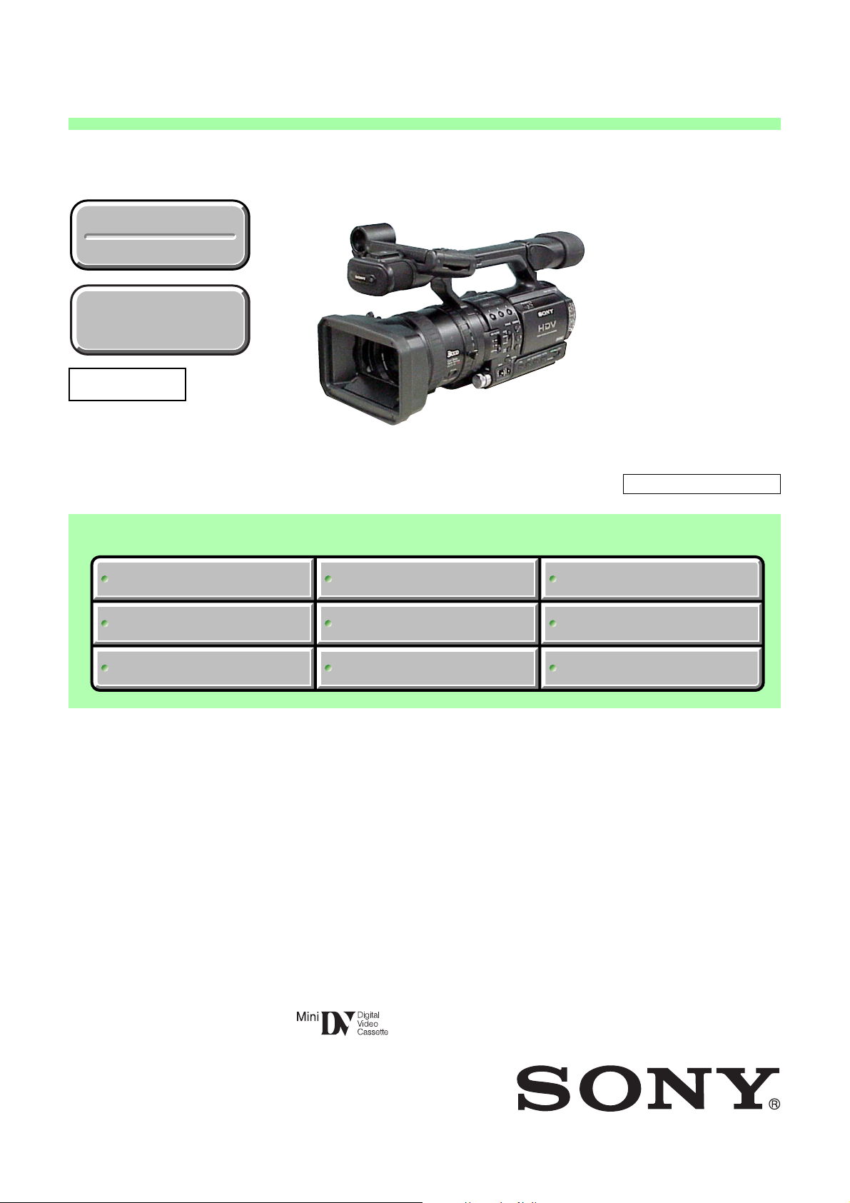
HVR Z1J
Table of contents
 Loading...
Sony HVR Z1J, HVR-Z1U, HVR-Z1N, HVR-Z1E, HVR-Z1P Service Manual
...
SERVICE MANUAL
DIGITAL VIDEO CAMERA RECORDER
• INSTRUCTION MANUAL is shown at the end of this document.
• Reference number search on printed wiring boards is available.
• TO TAKE OUT A CASSETTE WHEN NOT EJECT (FORCE EJECT)
Link
SERVICE NOTE
DISASSEMBLY
BLOCK DIAGRAMS
FRAME SCHEMATIC DIAGRAMS
SCHEMATIC DIAGRAMS
PRINTED WIRING BOARDS
REPAIR PARTS LIST
SPECIFICATIONS
ADJUSTMENT
SERVICE NOTE
DISASSEMBLY
BLOCK DIAGRAMS
FRAME SCHEMATIC DIAGRAMS
SCHEMATIC DIAGRAMS ADJUSTMENT
PRINTED WIRING BOARDS
REPAIR PARTS LIST
SPECIFICATIONS
Link
Revision History
Revision History
Ver. 1.9 2008.09
How to use
Acrobat Reader
How to use
Acrobat Reader
Sony EMCS Co.
2008I0800-1
©2008.09
Published by Kohda TEC
9-876-853-12
HVR-Z1J/Z1U/Z1N/Z1E/Z1P/Z1C
HVR-Z1J/Z1U/Z1N/
Z1E/Z1P/Z1C
RMT-841
HVR-Z1U
US Model
Canadian Model
HVR-Z1E
AEP Model
HVR-Z1C
Chinese Model
HVR-Z1N/Z1P
E Model
HVR-Z1J
Japanese Model
Z (Z311) MECHANISM
Revised-1
Replace the previously issued
SERVICE MANUAL 9-876-853-11
with this Manual.

— 2 —
HVR-Z1J/Z1U/Z1N/Z1E/Z1P/Z1C
SPECIFICATIONS
ENGLISH JAPANESE
ENGLISH JAPANESE
— 3 —
HVR-Z1J/Z1U/Z1N/Z1E/Z1P/Z1C
ENGLISH JAPANESE
ENGLISH JAPANESE

— 4 —
HVR-Z1J/Z1U/Z1N/Z1E/Z1P/Z1C
ENGLISH JAPANESE
ENGLISH JAPANESE
1. Check the area of your repair for unsoldered or poorly-soldered
connections. Check the entire board surface for solder splashes
and bridges.
2. Check the interboard wiring to ensure that no wires are
"pinched" or contact high-wattage resistors.
3. Look for unauthorized replacement parts, particularly
transistors, that were installed during a previous repair . Point
them out to the customer and recommend their replacement.
4. Look for parts which, through functioning, show obvious signs
of deterioration. Point them out to the customer and
recommend their replacement.
5. Check the B+ voltage to see it is at the values specified.
6. Flexible Circuit Board Repairing
• Keep the temperature of the soldering iron around 270˚C
during repairing.
• Do not touch the soldering iron on the same conductor of the
circuit board (within 3 times).
• Be careful not to apply force on the conductor when soldering
or unsoldering.
Unleaded solder
Boards requiring use of unleaded solder are printed with the lead-
free mark (LF) indicating the solder contains no lead.
(Caution: Some printed circuit boards may not come printed with
the lead free mark due to their particular size.)
: LEAD FREE MARK
Unleaded solder has the following characteristics.
• Unleaded solder melts at a temperature about 40°C higher than
ordinary solder.
Ordinary soldering irons can be used but the iron tip has to be
applied to the solder joint for a slightly longer time.
Soldering irons using a temperature regulator should be set to
about 350°C.
Caution: The printed pattern (copper foil) may peel away if the
heated tip is applied for too long, so be careful!
• Strong viscosity
Unleaded solder is more viscous (sticky, less prone to flow) than
ordinary solder so use caution not to let solder bridges occur such
as on IC pins, etc.
• Usable with ordinary solder
It is best to use only unleaded solder but unleaded solder may
also be added to ordinary solder.
SAFETY CHECK-OUT
After correcting the original service problem, perform the following
safety checks before releasing the set to the customer.
SAFETY-RELATED COMPONENT WARNING!!
COMPONENTS IDENTIFIED BY MARK 0 OR DOTTED LINE WITH
MARK 0 ON THE SCHEMATIC DIAGRAMS AND IN THE PARTS
LIST ARE CRITICAL TO SAFE OPERATION. REPLACE THESE
COMPONENTS WITH SONY PARTS WHOSE PART NUMBERS
APPEAR AS SHOWN IN THIS MANUAL OR IN SUPPLEMENTS
PUBLISHED BY SONY.
ATTENTION AU COMPOSANT AYANT RAPPORT
À LA SÉCURITÉ!
LES COMPOSANTS IDENTIFÉS PAR UNE MARQUE 0 SUR LES
DIAGRAMMES SCHÉMATIQUES ET LA LISTE DES PIÈCES SONT
CRITIQUES POUR LA SÉCURITÉ DE FONCTIONNEMENT. NE
REMPLACER CES COMPOSANTS QUE PAR DES PIÈSES SONY
DONT LES NUMÉROS SONT DONNÉS DANS CE MANUEL OU
DANS LES SUPPÉMENTS PUBLIÉS PAR SONY.
CAUTION :
Danger of explosion if battery is incorrectly replaced.
Replace only with the same or equivalent type.

— 5 —
HVR-Z1J/Z1U/Z1N/Z1E/Z1P/Z1C
ENGLISH JAPANESE
ENGLISH JAPANESE
1. 注意事項をお守りください。
サービスのとき特に注意を要する個所については,
キャビネット,シャーシ,部品などにラベルや捺印で
注意事項を表示しています。これらの注意書き及び取
扱説明書等の注意事項を必ずお守り下さい。
2. 指定部品のご使用を
セットの部品は難燃性や耐電圧など安全上の特性を
持ったものとなっています。従って交換部品は,使用
されていたものと同じ特性の部品を使用して下さい。
特に回路図,部品表に0印で指定されている安全上重要
な部品は必ず指定のものをご使用下さい。
3. 部品の取付けや配線の引きまわしはもとどおりに
安全上,チューブやテープなどの絶縁材料を使用した
り,プリント基板から浮かして取付けた部品がありま
す。また内部配線は引きまわしやクランパによって発
熱部品や高圧部品に接近しないよう配慮されています
ので,これらは必ずもとどおりにして下さい。
4. サービス後は安全点検を
サービスのために取外したネジ,部品,配線がもとど
おりになっているか,またサービスした個所の周辺を
劣化させてしまったところがないかなどを点検し,安
全性が確保されていることを確認して下さい。
5. チップ部品交換時の注意
• 取外した部品は再使用しないで下さい。
• タンタルコンデンサのマイナス側は熱に弱いため交
換時は注意して下さい。
サービス,点検時には次のことにご注意下さい。
注意
電池の交換は,正しく行わないと破裂する恐れがあり
ます。電池を交換する場合には必ず同じ型名の電池
又は同等品と交換してください。
6. フレキシブルプリント基板の取扱いについて
• コテ先温度を270℃前後にして行なって下さい。
• 同一パターンに何度もコテ先を当てないで下さい。
(3回以内)
• パターンに力が加わらないよう注意して下さい。
7. 無鉛半田について
無鉛半田を使用している基板には,無鉛(Lead Free)を
意味するレッドフリーマークがプリントされています。
(注意:基板サイズによっては,無鉛半田を使用して
いてもレッドフリーマークがプリントされて
いないものがあります)
:レッドフリーマーク
無鉛半田には,以下の特性があります。
• 融点が従来の半田よりも約40℃高い。
従来の半田こてをそのまま使用することは可能です
が,少し長めにこてを当てる必要があります。
温度調節機能のついた半田こてを使用する場合,約
350℃に設定して下さい。
注意: 半田こてを長く当てすぎると,基板のパター
ン(銅箔)がはがれてしまうことがあります
ので,注意して下さい。
• 粘性が強い
従来の半田よりも粘性が強いため,IC端子などが半田
ブリッジしないように注意して下さい。
• 従来の半田と混ぜて使用可能
無鉛半田には無鉛半田を追加するのが最適ですが,
従来の半田を追加しても構いません。

— 6 —
HVR-Z1J/Z1U/Z1N/Z1E/Z1P/Z1C
TABLE OF CONTENTS
1. SERVICE NOTE
1-1. SERVICE NOTE ·····························································1-1
1. NOTE FOR REPAIR ·······················································1-1
2. POWER SUPPLY DURING REPAIRS··························1-2
3. TO TAKE OUT A CASSETTE WHEN NOT EJECT
(FORCE EJECT) ·····························································1-2
1-2. SELF-DIAGNOSIS FUNCTION····································1-3
1. SELF-DIAGNOSIS FUNCTION····································1-3
2. SELF-DIAGNOSIS DISPLAY ·······································1-3
3. SELF-DIAGNOSIS CODE TABLE································1-4
2. DISASSEMBLY
2-1. DISASSEMBLY ······························································2-1
2-2. SERVICE POSITION ·····················································2-7
2-3. CIRCUIT BOARDS LOCATION ·································2-10
2-4. FLEXIBLE BOARDS LOCATION ······························2-12
3. BLOCK DIAGRAMS
3-1. OVERALL BLOCK DIAGRAM (1/6) ···························3-1
3-2. OVERALL BLOCK DIAGRAM (2/6) ···························3-3
3-3. OVERALL BLOCK DIAGRAM (3/6) ···························3-5
3-4. OVERALL BLOCK DIAGRAM (4/6) ···························3-7
3-5. OVERALL BLOCK DIAGRAM (5/6) ···························3-9
3-6. OVERALL BLOCK DIAGRAM (6/6) ·························3-11
3-7. POWER BLOCK DIAGRAM (1/4)······························3-13
3-8. POWER BLOCK DIAGRAM (2/4)······························3-15
3-9. POWER BLOCK DIAGRAM (3/4)······························3-17
3-10. POWER BLOCK DIAGRAM (4/4)······························3-19
4. PRINTED WIRING BOARDS AND
SCHEMATIC DIAGRAMS
4-1. FRAME PRINTED WIRING BOARD (1/2)··················4-1
FRAME PRINTED WIRING BOARD (2/2)··················4-3
4-2. SCHEMATIC DIAGRAMS
• CK-143 (FUNCTION KEY)
SCHEMATIC DIAGRAMS····························4-7
• FP-962 FLEXIBLE BOARD (IRIS DIAL)
SCHEMATIC DIAGRAM ······························4-7
• FP-963 FLEXIBLE BOARD (WB/GAIN SW)
SCHEMATIC DIAGRAM ······························4-7
• FP-965 FLEXIBLE BOARD (LID SW)
SCHEMATIC DIAGRAM ······························4-7
• FK-090 (VTR FUNCTION KEY)
SCHEMATIC DIAGRAM ······························4-9
• FP-959 FLEXIBLE BOARD (BATTERY)
SCHEMATIC DIAGRAM ···························· 4-11
• FP-960 FLEXIBLE BOARD (MIC SELECT)
SCHEMATIC DIAGRAM ···························· 4-11
• FP-961 FLEXIBLE BOARD (FUNCTION KEY, TALLY)
SCHEMATIC DIAGRAM ···························· 4-12
• FP-964 FLEXIBLE BOARD (DV TERMINAL)
SCHEMATIC DIAGRAM ···························· 4-11
• FP-971 FLEXIBLE BOARD (RELAY)
SCHEMATIC DIAGRAM ···························· 4-13
• FP-972 FLEXIBLE BOARD (RELAY)
SCHEMATIC DIAGRAM ···························· 4-15
• FP-978 FLEXIBLE BOARD (MIC TERMINAL)
SCHEMATIC DIAGRAM ···························· 4-15
• FP-974 FLEXIBLE BOARD (RELAY)
SCHEMATIC DIAGRAM ···························· 4-17
• FP-976 FLEXIBLE BOARD (RELAY)
SCHEMATIC DIAGRAM ···························· 4-19
• FP-977 FLEXIBLE BOARD (RELAY)
SCHEMATIC DIAGRAM ···························· 4-21
• FP-980 FLEXIBLE BOARD (RELAY, REAR IR)
SCHEMATIC DIAGRAM ···························· 4-23
• CONTROL SWITCH BLOCK (ZS5610)
SCHEMATIC DIAGRAM ···························· 4-23
• FP-975 FLEXIBLE BOARD (RELAY)
SCHEMATIC DIAGRAM ···························· 4-24
• FP-981 FLEXIBLE BOARD (RELAY)
SCHEMATIC DIAGRAM ···························· 4-25
• IF-122 (RELAY)
SCHEMATIC DIAGRAM ···························· 4-27
• FP-967 FLEXIBLE BOARD (MR SENSOR)
SCHEMATIC DIAGRAM ···························· 4-27
• SW-433 (PANEL REV)
SCHEMATIC DIAGRAM ···························· 4-28
• JK-275 (JACK)
SCHEMATIC DIAGRAM ···························· 4-29
• LB-106 (EVF BACK LIGHT)
SCHEMATIC DIAGRAM ···························· 4-31
• MA-431 (INT MIC AMP)
SCHEMATIC DIAGRAM ···························· 4-33
• MK-017 (FUNCTION KEY)
SCHEMATIC DIAGRAM ···························· 4-35
• FP-966 FLEXIBLE BOARD (AUTO LOCK)
SCHEMATIC DIAGRAM ···························· 4-36
• CONTROL SWITCH BLOCK (VV91010)
SCHEMATIC DIAGRAM ···························· 4-36
• MR-048 (1/2) (REC/PB RF AMP)
SCHEMATIC DIAGRAM ···························· 4-37
• MR-048 (2/2) (DRUM/CAPSTAN/LOADING MOTOR
DRIVE)
SCHEMATIC DIAGRAM ···························· 4-39
• PD-222 (LCD DRIVER, TIMING GENERATOR)
SCHEMATIC DIAGRAM ···························· 4-41
• SE-150 (PITCH/YAW SENSOR AMP)
SCHEMATIC DIAGRAM ···························· 4-43
• VA-119 (1/4) (AUDIO IN/OUT)
SCHEMATIC DIAGRAM ···························· 4-45
• VA-119 (2/4) (VIDEO IN/OUT)
SCHEMATIC DIAGRAM ···························· 4-47
• VA-119 (3/4) (Y. PB. PR. OUT AMP)
SCHEMATIC DIAGRAM ···························· 4-49
• VA-119 (4/4) (XLR INPUT)
SCHEMATIC DIAGRAM ···························· 4-51
• CONTROL SWITCH BLOCK (CF5610)
SCHEMATIC DIAGRAM ···························· 4-53
• CONTROL SWITCH BLOCK (PS5610)
SCHEMATIC DIAGRAM ···························· 4-54
• CD-522 (R.G.B-CH CCD IMAGER, S/H, AGC)
SCHEMATIC DIAGRAM ···························· 4-55
• DA-033 (DC/DC CONVERTER)
SCHEMATIC DIAGRAM ···························· 4-57
• DB-018 (1/2) (DC IN, CHARGE)
SCHEMATIC DIAGRAM ···························· 4-59
• DB-018 (2/2) (DC/DC CONVERTER)
SCHEMATIC DIAGRAM ···························· 4-61
• VC-367 (1/25) (CCD RF IN)
SCHEMATIC DIAGRAM ···························· 4-63
• VC-367 (2/25) (R.G.B-CH AGC, A/D CONV., TIMING
GENERATOR)
SCHEMATIC DIAGRAM ···························· 4-65
• VC-367 (3/25) (CAMERA RGB PROCESS)
SCHEMATIC DIAGRAM ···························· 4-67
• VC-367 (4/25) (LENS DRIVE)
SCHEMATIC DIAGRAM ···························· 4-69
• VC-367 (5/25) (LENS DRIVE CONTROL)
SCHEMATIC DIAGRAM ···························· 4-71
• VC-367 (6/25) (CAMERA CONTROL)
SCHEMATIC DIAGRAM ···························· 4-73

— 7 —
HVR-Z1J/Z1U/Z1N/Z1E/Z1P/Z1C
• VC-367 (7/25) (BASE BAND PROCESS)
SCHEMATIC DIAGRAM ···························· 4-75
• VC-367 (8/25) (OSD, D3 FILTER)
SCHEMATIC DIAGRAM ···························· 4-77
• VC-367 (9/25) (HDV VIDEO ENCODER)
SCHEMATIC DIAGRAM ···························· 4-79
• VC-367 (10/25) (64MBIT SDRAM (L/U))
SCHEMATIC DIAGRAM ···························· 4-81
• VC-367 (11/25) (HDV SIGNAL/RF SIGNAL PROCESS)
SCHEMATIC DIAGRAM ···························· 4-83
• VC-367 (12/25) (HDV VIDEO DECODER)
SCHEMATIC DIAGRAM ···························· 4-85
• VC-367 (13/25) (64MBIT Y/C-SDRAM)
SCHEMATIC DIAGRAM ···························· 4-87
• VC-367 (14/25) (I LINK INTERFACE)
SCHEMATIC DIAGRAM ···························· 4-89
• VC-367 (15/25) (DV/RF SIGNAL PROCESS)
SCHEMATIC DIAGRAM ···························· 4-91
• VC-367 (16/25) (VIDEO A/D CONV.)
SCHEMATIC DIAGRAM ···························· 4-93
• VC-367 (17/25) (EVF RGB DRIVER, TIMING
GENERATOR)
SCHEMATIC DIAGRAM ···························· 4-95
• VC-367 (18/25) (HDV AUDIO SIGNAL PROCESS)
SCHEMATIC DIAGRAM ···························· 4-97
• VC-367 (19/25) (AUDIO INPUT SELECT, AUDIO
CONVERTOR)
SCHEMATIC DIAGRAM ···························· 4-99
• VC-367 (20/25) (DS CONTROL)
SCHEMATIC DIAGRAM ·························· 4-101
• VC-367 (21/25) (FRONT CONTROL)
SCHEMATIC DIAGRAM ·························· 4-103
• VC-367 (22/25) (LSI CONTROL)
SCHEMATIC DIAGRAM ·························· 4-105
• VC-367 (23/25) (MECHA CONTROL)
SCHEMATIC DIAGRAM ·························· 4-107
• VC-367 (24/25) (CONNECTOR-1)
SCHEMATIC DIAGRAM ·························· 4-109
• VC-367 (25/25) (CONNECTOR-2)
SCHEMATIC DIAGRAM ·························· 4-111
• FP-228/467/826 FLEXIBLE BOARD
SCHEMATIC DIAGRAM ·························· 4-113
4-3. PRINTED WIRING BOARDS
• CK-143 (FUNCTION KEY)
PRINTED WIRING BOARD ····················· 4-119
• FK-090 (VTR FUNCTION KEY)
PRINTED WIRING BOARD ····················· 4-121
• FP-959 FLEXIBLE (BATTERY)
PRINTED WIRING BOARD ····················· 4-121
• FP-960 FLEXIBLE (MIC SELECT)
PRINTED WIRING BOARD ····················· 4-122
• FP-964 FLEXIBLE (DV TERMINAL)
PRINTED WIRING BOARD ····················· 4-123
• FP-971 FLEXIBLE (RELAY)
PRINTED WIRING BOARD ····················· 4-123
• FP-967 FLEXIBLE (MR SENSOR)
PRINTED WIRING BOARD ····················· 4-124
• FP-975 FLEXIBLE (RELAY)
PRINTED WIRING BOARD ····················· 4-124
• FP-978 FLEXIBLE (MIC TERMINAL)
PRINTED WIRING BOARD ····················· 4-125
• FP-980 FLEXIBLE (RELAY, REAR IR)
PRINTED WIRING BOARD ····················· 4-125
• FP-981 FLEXIBLE (RELAY)
PRINTED WIRING BOARD ····················· 4-127
• FP-977 FLEXIBLE (RELAY)
PRINTED WIRING BOARD ····················· 4-127
• FP-976 FLEXIBLE (RELAY)
PRINTED WIRING BOARD ····················· 4-128
• IF-122 (RELAY)
PRINTED WIRING BOARD ····················· 4-129
• JK-275 (JACK)
PRINTED WIRING BOARD ····················· 4-131
• FP-972 FLEXIBLE BOARD (RELAY)
PRINTED WIRING BOARD ····················· 4-131
• LB-106 (EVF BACK LIGHT)
PRINTED WIRING BOARD ····················· 4-133
• FP-974 FLEXIBLE BOARD (RELAY)
PRINTED WIRING BOARD ····················· 4-133
• MA-431 (INT MIC AMP)
PRINTED WIRING BOARD ····················· 4-135
• MK-017 (FUNCTION KEY)
PRINTED WIRING BOARD ····················· 4-137
• FP-228/467/826 FLEXIBLE
PRINTED WIRING BOARD ····················· 4-137
• MR-048 (REC/PB RF AMP, DRUM/CAPSTAN/
LOADING MOTOR DRIVE)
PRINTED WIRING BOARD ····················· 4-139
• PD-222 (LCD DRIVER, TIMING GENERATOR)
PRINTED WIRING BOARD ····················· 4-143
• SE-150 (PITCH/YAW SENSOR AMP)
PRINTED WIRING BOARD ····················· 4-147
• SW-433 (PANEL REV)
PRINTED WIRING BOARD ····················· 4-147
• VA-119 (AUDIO IN/OUT, VIDEO IN/OUT, Y. PB. PR.
OUT AMP)
PRINTED WIRING BOARD ····················· 4-149
• CD-522 (R.G.B-CH CCD IMAGER, S/H, AGC)
PRINTED WIRING BOARD ····················· 4-153
• DA-033 (DC/DC CONVERTER)
PRINTED WIRING BOARD ····················· 4-157
• DB-018 (DC IN, CHARGE, DC/DC CONVERTER)
PRINTED WIRING BOARD ····················· 4-161
• VC-367 (CCD RF IN, R.G.B-CH AGC, A/D CONV.,
TIMING GENERATOR, CAMERA RGB PROCESS,
LENS DRIVE, LENS DRIVE CONTROL, CAMERA
CONTROL, BASE BAND PROCESS, OSD, D3 FILTER,
HDV VIDEO ENCODER, 64MBIT SDRAM (L/U),
HDV SIGNAL/RF SIGNAL PROCESS, HDV VIDEO
DECODER, 64MBIT Y/C-SDRAM, I LINK
INTERFACE, DV/RF SIGNAL PROCESS, VIDEO A/D
CONV., EVF RGB DRIVER, TIMING GENERATOR,
HDV AUDIO SIGNAL PROCESS, AUDIO INPUT
SELECT, AUDIO CONVERTOR, DS CONTROL,
FRONT CONTROL, LSI CONTROL, MECHA
CONTROL, CONNECTOR-1, CONNECTOR-2)
PRINTED WIRING BOARD ····················· 4-165
4-4. WAVEFORMS ····························································4-169
4-5. MOUNTED PARTS LOCATION ······························· 4-173
5. REPAIR PARTS LIST
5-1. EXPLODED VIEWS ······················································ 5-3
5-1-1.OVERALL SECTION····················································· 5-3
5-1-2.CABINET (R) SECTION-1 ············································ 5-4
5-1-3.CABINET (R) SECTION-2 ············································ 5-5
5-1-4.CABINET (L) SECTION ················································ 5-6
5-1-5.HANDLE SECTION-1 ··················································· 5-7
5-1-6.HANDLE SECTION-2 ··················································· 5-8
5-1-7.LCD SECTION ······························································· 5-9
5-1-8.EVF SECTION ······························································ 5-10
5-1-9.CENTER SECTION ······················································ 5-11
5-1-10. MAIN BOARD SECTION (VA, VC, DA, DB) ··········5-12
5-1-11. LENS SECTION ························································ 5-13
5-1-12. TERMINAL CABINET SECTION···························· 5-14

— 8 —
HVR-Z1J/Z1U/Z1N/Z1E/Z1P/Z1C
5-1-13. BATTERY SECTION AND DV SECTION ···············5-15
5-1-14. MECHANISM DECK OVERALL (Z311) ················ 5-16
5-1-15. LS CHASSIS BLOCK ASSEMBLY ·························· 5-17
5-1-16. MECHANICAL CHASSIS BLOCK ASSEMBLY ···· 5-18
Checking supplied accessories. ··············································· 5-19
5-2. ELECTRICAL PARTS LIST ········································ 5-21
6. ADJUSTMENT
1. Before starting adjustment ··············································· 6-1
1-1. Adjusting items when replacing main parts and boards. ··· 6-2
6-1. CAMERA SECTION ADJUSTMENT ··························· 6-4
1-1. PREPARATIONS BEFORE ADJUSTMENT
(CAMERA SECTION) ··················································· 6-4
1-1-1.List of Service Tools ························································6-4
1-1-2.Preparations ·····································································6-6
1-1-3.Precaution ········································································6-8
1. Setting the Switch ···························································· 6-8
2. Order of Adjustments ······················································ 6-8
3. Subjects ··········································································· 6-8
1-2. INITIALIZATION OF 8, 9, A, B, C, D, E, F, 13, 14, 18,
19, 1A, 1B, 1C, 1D, 1E, 1F PAGE DATA ·······················6-9
1-2-1.INITIALIZATION OF A, B, D, 1A, 1B PAGE DATA···· 6-9
1. Initializing the A, B, D, 1A, 1B Page Data ····················· 6-9
2. Modification of A, B, D, 1A, 1B Page Data ···················· 6-9
3. A Page Table ····································································6-9
4. B Page Table ·································································· 6-10
5. D Page Table ··································································6-10
6. 1A Page Table ································································6-10
7. 1B Page Table ································································ 6-10
1-2-2.INITIALIZATION OF 8, C, 13, 18, 1C PAGE DATA ···· 6-11
1. Initializing the 8, C, 13, 18, 1C Page Data ····················6-11
2. Modification of 8, C, 13, 18, 1C Page Data ·················· 6-11
3. 8 Page Table ··································································· 6-12
4. C Page Table ·································································· 6-13
5. 13 Page Table ································································· 6-14
6. 18 Page Table ································································· 6-14
7. 1C Page Table ································································ 6-15
1-2-3.INITIALIZATION OF 9, 1D PAGE DATA ·················· 6-16
1. Initializing the 9, 1D Page Data ···································· 6-16
2. Modification of 9, 1D Page Data ··································· 6-16
3. 9 Page Table ··································································· 6-16
4. 1D Page Table ································································6-16
1-2-4.
INITIALIZATION OF E, F, 14, 19, 1E, 1F PAGE DATA ··
6-17
1. Initializing the E, F, 14, 19, 1E, 1F Page Data ·············· 6-17
2. Modification of E, F, 14, 19, 1E, 1F Page Data ············· 6-18
3. E Page Table (NTSC (60i) & PAL (50i) modes) ··········· 6-18
4. F Page Table (NTSC (60i) & PAL (50i) modes) ···········6-19
5. 14 Page Table (NTSC (60i) & PAL (50i) modes) ········· 6-20
6. 19 Page Table (NTSC (60i) & PAL (50i) modes) ········· 6-21
7. 1E Page Table (NTSC (60i) & PAL (50i) modes) ········· 6-21
8. 1F Page Table (NTSC (60i) & PAL (50i) modes) ·········6-22
1-3. CAMERA SYSTEM ADJUSTMENTS ························ 6-23
1. Origin Oscillation Check (NTSC (60i) & PAL (50i) modes)
(VC-367 board) ····························································· 6-24
2. HALL Adjustment (NTSC (60i) mode) ························ 6-25
3. MR Adjustment (NTSC (60i) mode) ····························· 6-26
4. Focus Ring Adjustment (NTSC (60i) mode)················· 6-27
5. Zoom Ring Adjustment (NTSC (60i) mode)················· 6-27
5-1. Zoom Ring Adjustment (1)············································ 6-27
5-2. Zoom Ring Adjustment (2)············································ 6-28
6. Flange Back Adjustment (NTSC (60i) mode) ··············· 6-29
6-1. Flange Back Adjustment (Using Minipattern Box or Flange
Back Adjustment Jig) ···················································· 6-29
6-2. Flange Back Adjustment (Using Flange Back Adjustment
Chart and Subject More Than 500m Away) ·················· 6-30
6-2-1.Flange Back Adjustment (1) ·········································· 6-30
6-2-2.Flange Back Adjustment (2) ·········································· 6-30
7. Flange Back Check (NTSC (60i) mode) ······················· 6-31
8. HALL Adjustment (PAL (50i) mode) ··························· 6-32
9. MR Adjustment (PAL (50i) mode) ································6-33
10. Focus Ring & Zoom Ring Adjustment
(PAL (50i) mode) ·························································· 6-33
11. Flange Back Adjustment (PAL (50i) mode) ··················6-34
12. Flange Back Check (PAL (50i) mode) ·························· 6-34
13. Picture Frame Setting
(NTSC (60i) & PAL (50i) modes) ································· 6-35
14. Auto White Balance Standard Data Input
(NTSC (60i) & PAL (50i) modes) ································· 6-36
14-1. Auto White Balance Standard Data Input ND OFF ······· 6-36
14-2. Auto White Balance Standard Data Input ND 1 ············ 6-36
14-3. Auto White Balance Standard Data Input ND 2
(NTSC (60i) & PAL (50i) modes) ································· 6-37
15. MAX GAIN Adjustment
(NTSC (60i) & PAL (50i) modes) ································· 6-37
16. LV Standard Data Input
(NTSC (60i) & PAL (50i) modes) ································· 6-38
17. Auto White Balance Adjustment
(NTSC (60i) & PAL (50i) modes) ································· 6-38
17-1. Auto White Balance Adjustment ND OFF ····················6-38
17-2. Auto White Balance Adjustment ND 1 ························· 6-39
17-3. Auto White Balance Adjustment ND 2 ························· 6-39
18. Color Reproduction Adjustment
(NTSC (60i) & PAL (50i) modes) ································· 6-40
18-1. Color Reproduction Adjustment ND OFF····················· 6-40
18-2. Color Reproduction Adjustment ND 1 ·························· 6-41
18-3. Color Reproduction Adjustment ND 2 ·························· 6-41
19. White Balance Check
(NTSC (60i) & PAL (50i) modes) ································· 6-42
19-1. White Balance Check ND OFF ·····································6-42
19-2. White Balance Check ND 1 ·········································· 6-43
19-3. White Balance Check ND 2 ·········································· 6-45
20. Color Reproduction Check HD STD γ
(NTSC (60i) & PAL (50i) modes) ································· 6-45
20-1. Color Reproduction Check ND OFF HD STD γ ··········· 6-45
20-2. Color Reproduction Check ND 1 HD STD γ ················· 6-46
20-3. Color Reproduction Check ND 2 HD STD γ ················ 6-46
21. Color Reproduction Check HD CINE γ
(NTSC (60i) & PAL (50i) modes) ································· 6-47
21-1. Color Reproduction Check ND OFF HD CINE γ ·········· 6-47
21-2. Color Reproduction Check ND 1 HD CINE γ ···············6-48
21-3. Color Reproduction Check ND 2 HD CINE γ ···············6-48
22. Color Reproduction Check SD STD γ
(NTSC (60i) & PAL (50i) modes) ································· 6-49
22-1. Color Reproduction Check ND OFF SD STD γ ···········6-49
22-2. Color Reproduction Check ND 1 SD STD γ·················· 6-50
22-3. Color Reproduction Check ND 2 SD STD γ·················· 6-50
23. Color Reproduction Check SD CINE γ
(NTSC (60i) & PAL (50i) modes) ································· 6-51
23-1. Color Reproduction Check ND OFF SD CINE γ ·········· 6-51
23-2. Color Reproduction Check ND 1 SD CINE γ ················ 6-52
23-3. Color Reproduction Check ND 2 SD CINE γ ················ 6-52
24. PSD Sensor Gain Adjustment
(NTSC (60i) & PAL (50i) modes) ································· 6-53
24-1. PSD Sensor Gain Adjustment (NTSC (60i) mode) (1) ···· 6-53
24-2. PSD Sensor Gain Adjustment (NTSC (60i) mode) (2) ···· 6-54
24-3. PSD Sensor Gain Adjustment (PAL (50i) mode) ·········· 6-55
25. Angular Velocity Sensor Sensitivity Adjustment
(NTSC (60i) & PAL (50i) modes) ································· 6-56
25-1. Angular Velocity Sensor Sensitivity Adjustment
(NTSC (60i) mode) ·······················································6-56
25-2. Angular Velocity Sensor Sensitivity Adjustment ··········· 6-57
1-4. COLOR ELECTRONIC VIEWFINDER SYSTEM
ADJUSTMENT ·····························································6-58
1. VCO Adjustment (VC-367 board) ································ 6-58

— 9 —
HVR-Z1J/Z1U/Z1N/Z1E/Z1P/Z1C
2. Backlight Adjustment (VC-367 board) ························· 6-59
3. PSIG Level Adjustment (VC-367 board) ······················ 6-59
4. VCOM Level Adjustment (VC-367 board) ··················· 6-60
5. RGB AMP Adjustment (VC-367 board) ······················ 6-60
6. Contrast Adjustment (VC-367 board) ··························· 6-61
7. White Balance Adjustment (VC-367 board) ·················6-61
1-5. LCD SYSTEM ADJUSTMENT ···································6-62
1. LCD Automatic Adjustment (PD-222 board) ················6-62
2. Contrast Adjustment (HD) (PD-222 board) ·················· 6-63
3. V COM Adjustment (PD-222 board) ···························· 6-63
4. Sample Hold Phase Adjustment
(PD-222 board) ······························································6-64
5. Transmissive Mode White Balance Adjustment
(PD-222 board) ······························································6-64
6. Reflective Mode White Balance Adjustment
(PD-222 board) ······························································6-65
6-2. MECHANISM SECTION ADJUSTMENT·················· 6-66
2-1. Preparations for Check, Adjustment and Replacement of
Mechanism Block ·························································· 6-66
2-1-1.Cassette Compartment Assy, Damper Assy ··················6-66
2-2. Periodic Inspection and Maintenance
2-2-1.Rotary Drum Cleaning ·················································· 6-67
2-2-2.Tape Path System Cleaning (Refer to Fig. 6-2-2.) ········ 6-67
2-2-3.Periodic Inspection List ·················································6-68
2-2-4.Mode Selector II Operating Procedure ·························· 6-69
2-4-1.Introduction ··································································· 6-69
2-4-2.Operation ·······································································6-70
2-4-3.Mechanism Status (Position) Transition Table Using
Mode Selector II ····························································6-72
2-4-4.Battery Alarm Indication ··············································· 6-70
2-3. Check, Adjustment and Replacement of
Mechanical Parts ··························································· 6-73
2-3-1.Flowchart of Replacement of Mechanical Parts ············ 6-73
2-3-2.Drum ·············································································· 6-75
2-3-3.Cassette Compartment Assy ·········································· 6-76
2-3-4.TG7 Support ··································································6-77
2-3-5.Motor Holder Block Assy and L Motor Block Assy ····· 6-78
2-3-6.MIC Terminal (MIC902) ···············································6-79
2-3-7.LED (D901) ··································································· 6-80
2-3-8.Retainer Plate ································································6-81
2-3-9.T Reel Table Assy ··························································6-82
2-3-10. Brake (S) and Release Rack (S) ·································· 6-83
2-3-11. Band Adjuster, S Reel Table Assy and
TG2 Arm Block Assy ················································· 6-84
2-3-12. ULE Brake Assy ························································· 6-85
2-3-13. Cassette Positioning (S) ··············································6-86
2-3-14. TG7 Arm Block Assy and Pinch Arm Assy ················6-87
2-3-15. TG7 ············································································· 6-88
2-3-16. Gooseneck Gear Assy ·················································6-89
2-3-17. LS Guide Retainer and LS Cam Plate ························ 6-90
2-3-18. LS Chassis Block Assy and
Mechanical Chassis Block Assy ································· 6-91
2-3-19. Brake (T) Block Assy ················································· 6-93
2-3-20. END Sensor (Q901) ···················································· 6-94
2-3-21. TOP Sensor (Q902)·····················································6-95
2-3-22. C-IN Switch (S903), S Reel Sensor (H901) and
T Reel Sensor (H902) ····················································6-96
2-3-23. Guide Rail ···································································6-97
2-3-24. Conversion Gear ························································· 6-98
2-3-25. Coaster (S) Block Assy and
Coaster (T) Block Assy ·············································· 6-99
2-3-26. TG5 Roller Assy and GL Gear (T) ··························· 6-100
2-3-27. TG2 Cam Plate Assy (N) ·········································· 6-101
2-3-28. LS Arm Assy ····························································· 6-102
2-3-29. M Slider Assy (1) ······················································ 6-103
2-3-30. M Slider Assy (2) ······················································ 6-104
2-3-31. EJ Arm ······································································ 6-105
2-3-32. Cam Gear and GL Driving········································ 6-106
2-3-33. Rotary Encoder (S902) ············································· 6-107
2-3-34. FP-228 Flexible Board (DEW SENSOR) and
FP-467 Flexible Board ············································· 6-108
2-4. Adjustment ·································································· 6-109
2-4-1.FWD Position Adjustment···········································6-109
2-4-2.Reel Torque Check ······················································ 6-109
2-4-3.LS Cam Plate Position Adjustment ·····························6-110
2-4-4.Tape Path Adjustment ·················································· 6-111
6-3. VIDEO SECTION ADJUSTMENT···························· 6-115
3-1. PREPARATIONS BEFORE ADJUSTMENTS ·········· 6-115
3-1-1.Equipment to Required ················································ 6-115
3-1-2.Precautions on Adjusting ············································· 6-116
3-1-3.Adjusting Connectors ··················································6-117
3-1-4.Connecting the Equipment ·········································· 6-117
3-1-5.Alignment Tapes ··························································6-118
3-1-6.Input/Output Level and Impedance ·····························6-118
3-2. SYSTEM CONTROL SYSTEM ADJUSTMENT ······6-119
1. Initialization of 8, 9, A, B, C, D, E, F, 13, 14, 18, 19, 1A,
1B, 1C, 1D, 1E, 1F Page Data ····································· 6-119
2. Serial No. Input ··························································· 6-119
3-3. SERVO AND RF SYSTEM ADJUSTMENT ·············6-121
1. Cap FG Duty Adjustment (VC-367 Board)················· 6-121
2. Switching Position Adjustment (VC-367 Board) ········ 6-121
3. Error Rate Check ·························································6-122
3-1. Preparations before adjustments ·································· 6-122
3-2. Error Rate Check ·························································6-122
3-3. Processing after Completing Adjustments ·················· 6-122
3-4. VIDEO SYSTEM ADJUSTMENTS··························· 6-123
1.
S VIDEO OUT Y Level Adjustment (VC-367 Board) ···
6-124
2. S VIDEO OUT Chroma Level Adjustment
(VC-367 Board) ··························································· 6-124
3. VIDEO OUT Y, Chroma Level Check
(VC-367 Board) ··························································· 6-125
4. COMPONENT OUTPUT Level Adjustment
(VC-367 Board) ··························································· 6-126
3-5. AUDIO SYSTEM ADJUSTMENTS ·························· 6-127
1. Playback Level Check ·················································6-128
2. Overall Level Characteristics Check ···························6-128
3. Camera E-E Audio Level Check (1) ···························· 6-128
4. Camera E-E Audio Level Check (2) ···························· 6-128
6-4. SERVICE MODE ························································ 6-129
4-1. ADJUSTMENT REMOTE COMMANDER ··············6-129
1. Using the adjustment remote commander ···················6-129
2. Precautions upon using ················································ 6-129
the adjustment remote commander ······························ 6-129
4-2. DATA PROCESS························································· 6-130
4-3. SERVICE MODE ························································ 6-131
1. Setting the Test Mode ··················································6-131
2. Emergence Memory Address (Mechanism section) ···· 6-131
2-1. EMG Code (Emergency Code) ··································· 6-131
2-2. MSW Code ··································································6-132
3. Bit value discrimination ·············································· 6-133
4. Switch check (1) ··························································6-133
5. Switch check (2) ··························································6-133
6. Switch check (3) ··························································6-133
7. Switch check (4) ··························································6-134
8. Switch check (5) ··························································6-134
9. LED check ···································································6-135
10. Record of Use check (1) ··············································6-135
11. Record of Use check (2) ··············································6-135
12. Record of Self-diagnosis check ···································6-136
SELF-DIAGNOSIS CODE TABLE ······································ 6-137
* Color reproduction frame is shown on page 6-138, 139.
1-1
HVR-Z1J/Z1U/Z1N/Z1E/Z1P/Z1C
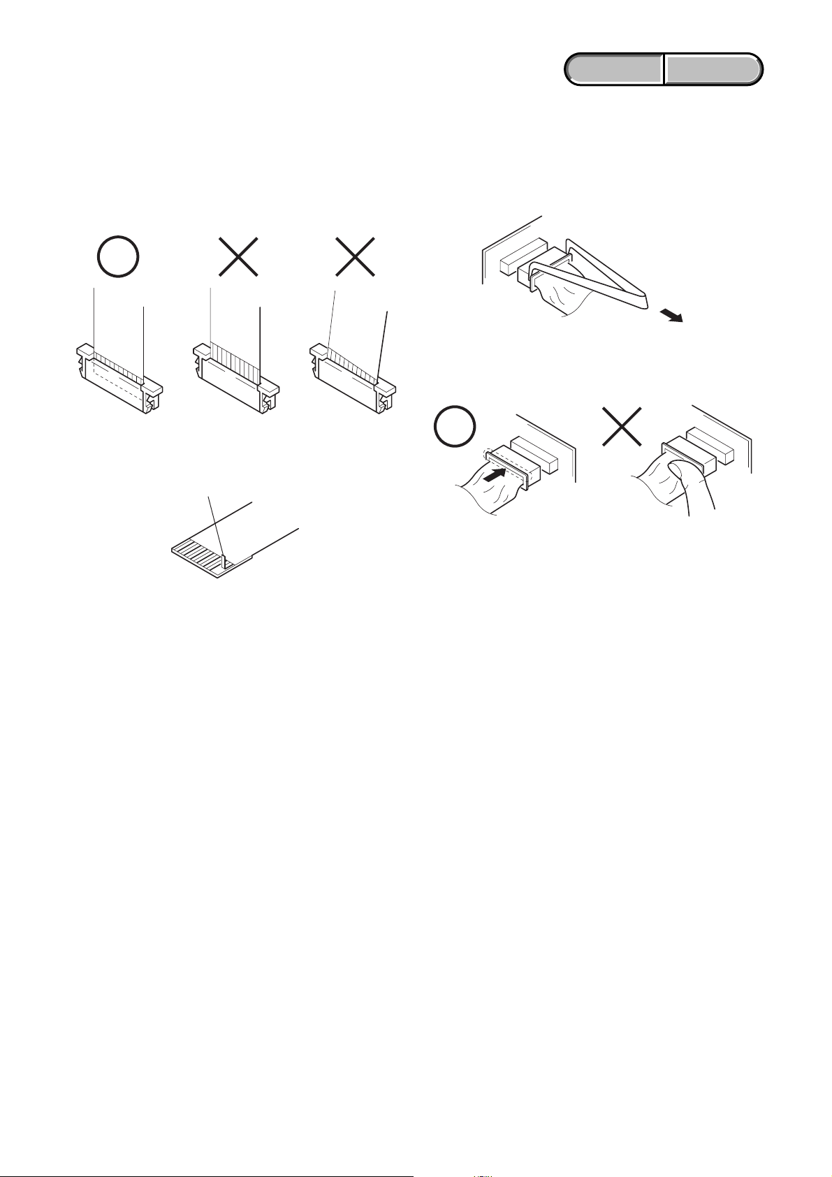
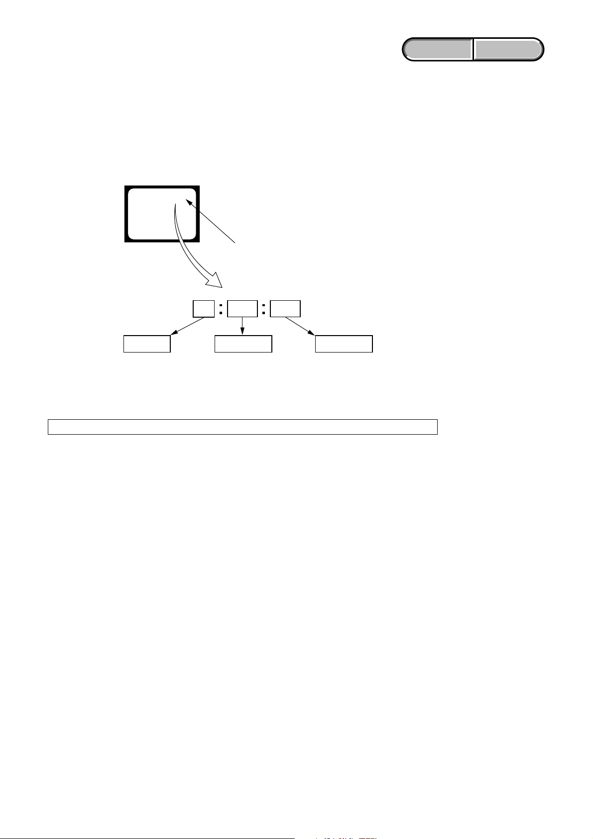
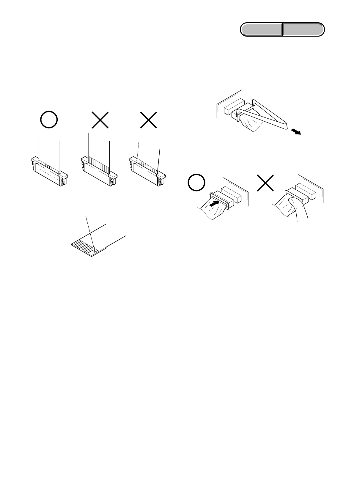
Make sure that the flat cable and flexible board are not cracked of
bent at the terminal.
Do not insert the cable insufficiently nor crookedly.
Cut and remove the part of gilt
which comes off at the point.
(Take care that there are
some pieces of gilt left inside)
When remove a connector, don't pull at wire of connector.
Be in danger of the snapping of a wire.
When installing a connector, don't press down at wire of connector.
Be in danger of the snapping of a wire.
1-1. SERVICE NOTE
1. NOTE FOR REPAIR
ENGLISH JAPANESE
ENGLISH JAPANESE
1. SERVICE NOTE
1-2
HVR-Z1J/Z1U/Z1N/Z1E/Z1P/Z1C
ENGLISH JAPANESE
ENGLISH JAPANESE
2. POWER SUPPLY DURING REPAIRS
In this unit, about 10 seconds after power is supplied to the battery terminal using the regulated power supply (8.4V), the power is shut off so
that the unit cannot operate.
This following three methods are available to prevent this. Take note of which to use during repairs.
Method 1:
Use the AC adapter and the connecting cord that are supplied with the equipment.
Method 2:
When you want to supply the power from a regulated power supply unit to the BATTERY terminal of this equipment, connect the adjustment
remote commander RM-95 (J-6082-053-B) to the LANC terminal of this equipment. Then set the HOLD switch to the ADJ position.
Method 3:
Note: The Method 3 should be used only during repair. Do not use the Method 3 during the ordinary operation.
Connect a usable AC adapter: AC-L10 or AC-L15. (There are type A and type B. Both types can be used.)
1. Set the MIC PHANTOM switch to OFF. (Power consumption should be minimal because AC adapter has the limited capacity.)
2. Remove the DC IN cover and connect the AC adapter.
3. Connect the adjustment remote commander RM-95 (J-6082-053-B) to the LANC terminal of this equipment, and set the HOLD switch
to the ADJ position. Turn on the power of the camera.
4. When the data are set as described below, the equipment can be operated on the AC adapter even if you unplug the adjustment remote
commander.
1)Select page: 0, address: 01, and set data: 01.
2)Select page: 0, address: 10, and set data: 00.
3)Select page: D, address: 23, set data: AF, and press the PAUSE button of the adjustment remote commander.
5. Be sure to return the data setup to the original setup as shown below upon completion of the adjustment.
1)Select page: 0, address: 01, and set data: 01.
2)Select page: 0, address: 10, and set data: 00.
3)Select page: D, address: 23, set data: FF, and press the PAUSE button of the adjustment remote commander.
4)Select page: 0, address: 01, and set data: 00.
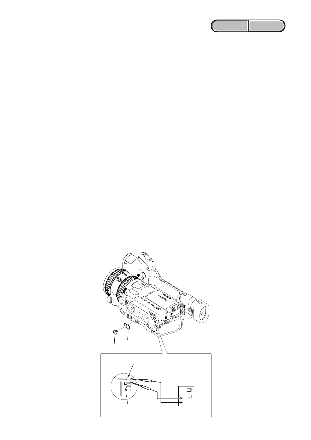
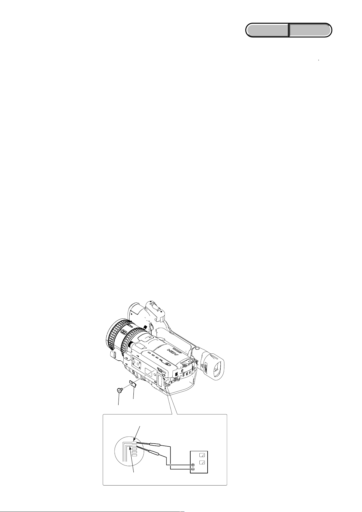
3. TO TAKE OUT A CASSETTE WHEN NOT EJECT (FORCE EJECT)
1 Remove the power supply (Battery and AC power adaptor).
2 Open the cassette lid.
3 Remove the MD lid.
4 Supply +4.5V between the LM UNLOAD terminal and the LM LOAD terminal from the DC power supply and unload the cassete.
DC power supply
(+4.5V)
LM load
LM unload
MD lid
Screw (M2x4)
Ver. 1.7 2007. 10
1-3
HVR-Z1J/Z1U/Z1N/Z1E/Z1P/Z1C
ENGLISH JAPANESE
ENGLISH JAPANESE
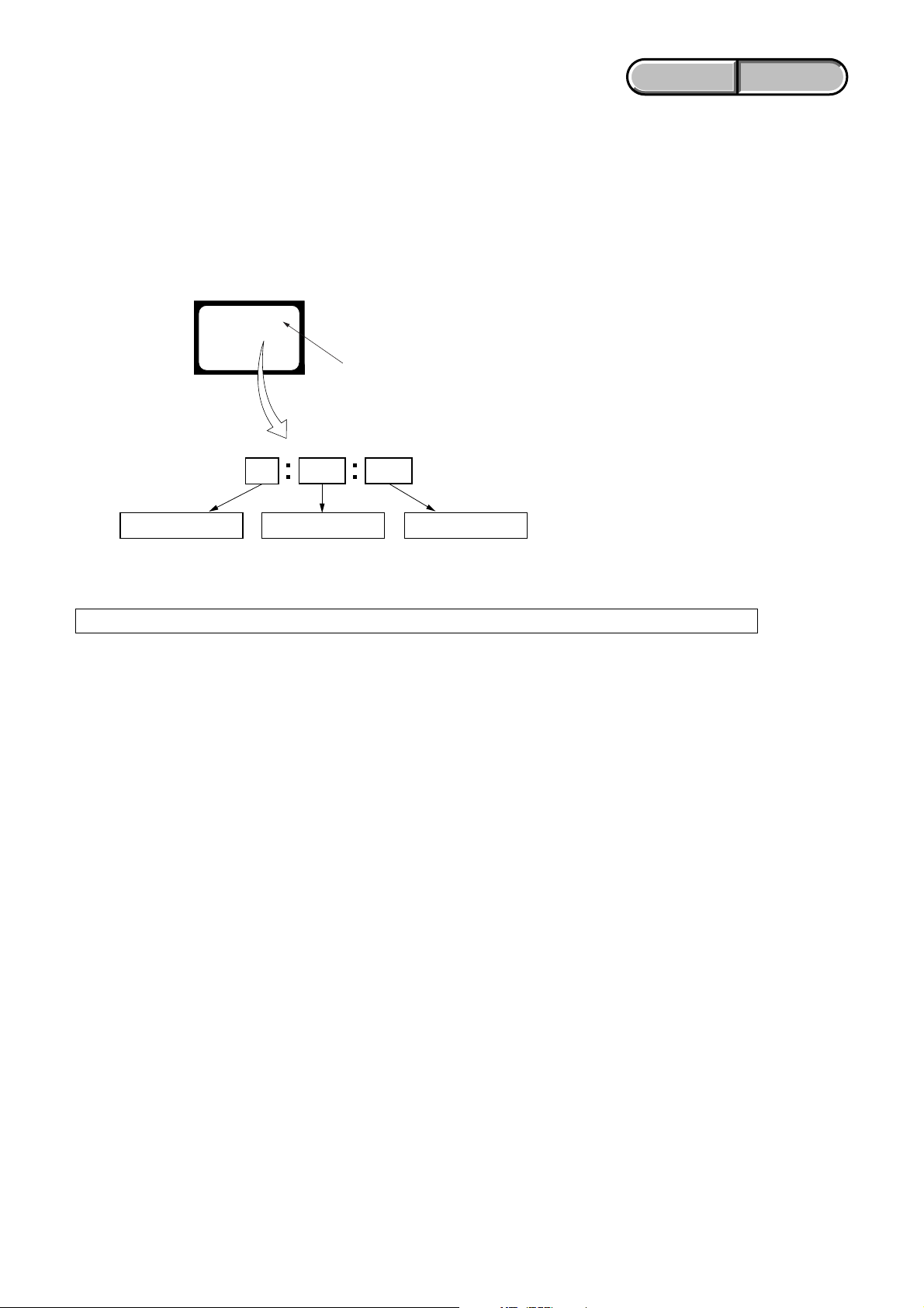
1-2. SELF-DIAGNOSIS FUNCTION
1. SELF-DIAGNOSIS FUNCTION
When problems occur while the unit is operating, the self-diagnosis
function starts working, and displays on the viewfinder, or LCD
screen what to do.
Details of the self-diagnosis functions are provided in the Instruction
manual.
2. SELF-DIAGNOSIS DISPLAY
When problems occur while the unit is operating, the counter of the
viewfinder or LCD screen consists of an alphabet and 4-digit number ,
which blinks at 3.2Hz. This 5-character display indicates the
“repaired by:”, “block” in which the problem occurred, and “detailed
code” of the problem.
Note: The self-diagnosis display data will be kept even if the lithium battery (BT591 of FP-959 flexible) is removed.
1 1
3 1C
Repaired by:
Refer to page 1-4.
Self-diagnosis Code Table.
Indicates the appropriate
step to be taken.
E.g.
31 ....Reload the tape.
32 ....Turn on power again.
Block
Detailed Code
Blinks at 3.2Hz
C : Corrected by customer
H : Corrected by dealer
E : Corrected by service
engineer
Viewfinder or LCD screen
C : 3 1 : 1 1

1-4
HVR-Z1J/Z1U/Z1N/Z1E/Z1P/Z1C
ENGLISH JAPANESE
ENGLISH JAPANESE
3. SELF-DIAGNOSIS CODE TABLE
C
C
C
C
C
C
C
C
C
C
C
C
C
C
C
C
C
C
C
C
C
C
C
E
E
E
E
E
E
Block
Function
04
21
22
31
31
31
31
31
31
31
31
31
31
32
32
32
32
32
32
32
32
32
32
20
61
61
61
62
62
Detailed
Code
00
00
00
10
11
20
21
22
23
24
30
40
42
10
11
20
21
22
23
24
30
40
42
00
00
10
11
00
01
Symptom/State
Non-standard battery is used.
Condensation.
Video head is dirty.
LOAD direction. Loading does not
complete within specified time
UNLOAD direction. Loading does not
complete within specified time
T reel side tape slacking when unloading
.
Winding S reel fault when counting the
rest of tape.
T reel fault.
S reel fault.
T reel fault.
FG fault when starting capstan.
FG fault when starting drum.
FG fault during normal drum operations.
LOAD direction loading motor time-
out.
UNLOAD direction loading motor
time-out.
T reel side tape slacking when
unloading.
Winding S reel fault when counting the
rest of tape.
T reel fault.
S reel fault.
T reel fault.
FG fault when starting capstan.
FG fault when starting drum
FG fault during normal drum
operations
Data on A page or D page are rewriten.
Difficult to adjust focus
(Cannot initialize focus.)
Zoom operations fault
(Cannot initialize zoom lens.)
The abnormalities in initialization of the
focus lens and the abnormalities in
initialization of the zoom lens occurred
simultaneously.
Steadyshot function does not work well.
(With pitch angular velocity sensor output
stopped.)
Steadyshot function does not work well.
(With yaw angular velocity sensor output
stopped.)
Self-diagnosis Code
Repaired by:
Correction
Use the info LITHIUM battery.
Remove the cassette, and insert it again after one hour.
Clean with the optional cleaning cassette.
Load the tape again, and perform operations from the beginning.
Load the tape again, and perform operations from the beginning.
Load the tape again, and perform operations from the beginning.
Load the tape again, and perform operations from the beginning.
Load the tape again, and perform operations from the beginning.
Load the tape again, and perform operations from the beginning.
Load the tape again, and perform operations from the beginning.
Load the tape again, and perform operations from the beginning.
Load the tape again, and perform operations from the beginning.
Load the tape again, and perform operations from the beginning.
Remove the battery or power cable, connect, and perform
operations from the beginning.
Remove the battery or power cable, connect, and perform
operations from the beginning.
Remove the battery or power cable, connect, and perform
operations from the beginning.
Remove the battery or power cable, connect, and perform
operations from the beginning.
Remove the battery or power cable, connect, and perform
operations from the beginning.
Remove the battery or power cable, connect, and perform
operations from the beginning.
Remove the battery or power cable, connect, and perform
operations from the beginning.
Remove the battery or power cable, connect, and perform
operations from the beginning.
Remove the battery or power cable, connect, and perform
operations from the beginning.
Remove the battery or power cable, connect, and perform
operations from the beginning.
Make data A page and D page correct value.
Inspect the lens block focus MR sensor (Pin qd, qf of CN1501 of
VC-367 board) when focusing is performed when the focus ring is
rotated in the focus manual mode, and the focus motor drive circuit
(IC1702 of VC-367 board) when the focusing is not performed.
Inspect the lens block zoom MR sensor (
Pin ra, rs of CN1501 of
VC-367 board
) when zooming is performed when the zoom switch
is operated and the zoom motor drive circuit (IC1702 of VC-367
board) when zooming is not performed.
Check whether the flexible board of the lens is broken, and check
whether it is inserted imperfectly. If there is no problem in the
flexible board, inspect the focus/zoom motor drive circuit (IC1702
of VC-367 board).
Inspect pitch angular velocity sensor (SE401 of SE-150 board)
peripheral circuits.
Inspect yaw angular velocity sensor (SE402 of SE-150 board)
peripheral circuits.
1-5
HVR-Z1J/Z1U/Z1N/Z1E/Z1P/Z1C
SECTION 1
SERVICE NOTE
1-1. サービスノート
1. 修理時の注意
フラットケーブルおよびフレキシブル基板の端子面に欠け,
折れ等がないことを確認する。
また,コネクタへの接続は,差し込み不足や斜め差しになら
ないように注意する。
線材部(極細)を押えながらコネクタを差し込むと,線材
部(極細)が断線する恐れがありますので,絶対に線材部
(極細)には負担をかけないで下さい。
コネクタを取り外す時に,線材部(極細)を持って引っ張
る
と断線する恐れがありますので,絶対に線材部(極細)
を
持って引っ張らないで下さい。
先端が剥がれたメッキ部はカットして除去する。
(メッキ破片がコネクタ内に残っている場合もあるので注意)
ENGLISH JAPANESE
ENGLISH JAPANESE
1-6
HVR-Z1J/Z1U/Z1N/Z1E/Z1P/Z1C
ENGLISH JAPANESE
ENGLISH JAPANESE
2. 修理/調整時の電源供給について
本機では、安定化電源(8.4Vdc)からバッテリー端子に電源を供給した場合、約10秒後にシャットオフし、動作しなくな
り
ます。
これを避けるため、下記のいずれかの方法を用いてください。
方法1:
本機付属のACアダプタと接続コードを使用する。
方法2:
安定化電源からバッテリー端子に電源を供給する場合は、調整リモコンRM-95(J-6082-053-B)を本気のLANC端子に接続
し、HOLDスイッチをADJ側にする。
方法3:
注意:この操作は修理時のみの対応方法です。一般動作時には使用しないで下さい。
使用可能なACアダプタ:AC-L10、L15(A、Bタイプあり。いずれも使用可)
1.MICPHANTOMスイッチをOFFにする。(ACアダプタ容量の余裕がないので消費電力を最小にする必要がある。)
2.DCINカバーをはずしACアダプタを接続する。
3.本機のLANC端子に調整リモコンRM-95(J-6082-053-B)を接続してADJ側に設定、カメラ電源を入れる。
4.下記のようにデータを設定すれば、調整リモコンを抜いてもACアダプタを使用して動作可能です。
1)ページ:0、アドレス:01、データ:01にセット
2)ページ:0、アドレス:10、データ:00にセット
3)ページ:D、アドレス:23、データ:AFにセットし調整リモコンのPAUSEボタンを押す。
5.調整後下記のようにデータ設定を必ず元の状態に戻す。
1)ページ:0、アドレス:01、データ:01にセット
2)ページ:0、アドレス:10、データ:00にセット
3)ページ:D、アドレス:23、データ:FFにセットし調整リモコンの PAUSE ボタンを押す。
4)ページ:0、アドレス:01、データ:00にセットする。
3. イジェクトしない時のカセット取出し方法(強制イジェクト)
1 電源(バッテリーとAC電源アダプター)を外す。
2 カセット蓋を開く。
3 MD蓋を外す。
4 DC電源より+4.5VをLMUNLOAD端子とLMLOAD端子の間に加え、アンローディングさせる。
MD 蓋
ねじ (M2X4)
LM LOAD 端子
LM UNLOAD 端子
DC 電源
(+4.5V)
Ver. 1.7 2007. 10
1-7
HVR-Z1J/Z1U/Z1N/Z1E/Z1P/Z1C
ENGLISH JAPANESE
ENGLISH JAPANESE
1-2. 自己診断機能
1. 自己診断機能について
本機の動作に不具合が生じたとき,自己診断機能が働き,
ビューファインダまたはLCD画面に,どう処置したらよいか
判断できる表示を行ないます。自己診断機能については取扱
説明書にも掲載されています。
2. 自己診断表示
本機の動作に不具合が生じたとき,ビューファインダまたは
LCD画面のカウンタ表示部分がアルファベットと数字の4桁
表示になり,3.2Hzで点滅します。この5文字の表示によ
っ
て,対応者分類および不具合の生じたブロックの分類,不具
合の詳細コードを示します。
注意:「自己診断表示」データはリチウム電池 (FP-959フレキシブル基板 (BT591)) を外しても消えません。
1 1
3 1C
対応者分類
「3. 自己診断コード表」
参照(1-8ページ)
ブロック分類
詳細コード
C:お客さま自身で対応
H:販売店で対応
E:サービスエンジニア
で対応
対応方法の違いにより分類
例 31…テープを入れ直す
32…電源を入れ直す
ビューファインダまたはLCD画面
3.2Hz点滅
C : 3 1 : 1 1
1-8E
HVR-Z1J/Z1U/Z1N/Z1E/Z1P/Z1C
ENGLISH JAPANESE
ENGLISH JAPANESE
3. 自己診断コード表
C
C
C
C
C
C
C
C
C
C
C
C
C
C
C
C
C
C
C
C
C
C
C
C
E
E
E
E
E
ブロック
機能
04
21
22
31
31
31
31
31
31
31
31
31
31
32
32
32
32
32
32
32
32
32
32
20
61
61
61
62
62
詳細
コード
00
00
00
10
11
20
21
22
23
24
30
40
42
10
11
20
21
22
23
24
30
40
42
00
00
10
11
00
01
症状/状態
インフォリチウム以外のバッテリを
使用している
結露している
ビデオヘッドが汚れている
LOAD方向,ローディング所定時間
内終了せず
UNLOAD方向,ローディング所定
時間内終了せず
UNLOAD時,Tリール側テープ弛み
テープ残量計算時,Sリール巻取り異常
Tリール異常
Sリール異常
Tリール異常
キャプスタン起動時FG異常
ドラム起動時FG異常
ドラム定常時FG異常
LOAD方向,ローディングモータ所
定時間動作せず
UNLOAD方向,ローディングモー
タ所定時間動作せず
UNLOAD時,Tリール側テープ弛み
テープ残量計算時,Sリール巻取り異常
Tリール異常
Sリール異常
Tリール異常
キャプスタン起動時FG異常
ドラム起動時FG異常
ドラム定常時FG異常
Aページ,Dページのデータが書き換
えられている。
フォーカスが合いにくい
(フォーカスの初期化ができない)
ズーム動作の異常(ズームレンズの
初期化ができない)
フォーカスレンズ初期化異常、
ズームレンズ初期化異常の同時発生
手振れ補正が効きにくい
(PITCH角速度センサ出力張り付き)
手振れ補正が効きにくい
(YAW角速度センサ出力張り付き)
自己診断コード
対応/方法
インフォリチウムバッテリを使用する
カセットを取り出して,約1時間してからもう一度入れ直す
別売のクリーニングカセットできれいにする
テープを入れ直し,再度操作し直す
テープを入れ直し,再度操作し直す
テープを入れ直し,再度操作し直す
テープを入れ直し,再度操作し直す
テープを入れ直し,再度操作し直す
テープを入れ直し,再度操作し直す
テープを入れ直し,再度操作し直す
テープを入れ直し,再度操作し直す
テープを入れ直し,再度操作し直す
テープを入れ直し,再度操作し直す
バッテリまたは電源ケーブルを外して付け直し,再度操作し直す
バッテリまたは電源ケーブルを外して付け直し,再度操作し直す
バッテリまたは電源ケーブルを外して付け直し,再度操作し直す
バッテリまたは電源ケーブルを外して付け直し,再度操作し直す
バッテリまたは電源ケーブルを外して付け直し,再度操作し直す
バッテリまたは電源ケーブルを外して付け直し,再度操作し直す
バッテリまたは電源ケーブルを外して付け直し,再度操作し直す
バッテリまたは電源ケーブルを外して付け直し,再度操作し直す
バッテリまたは電源ケーブルを外して付け直し,再度操作し直す
バッテリまたは電源ケーブルを外して付け直し,再度操作し直す
Aページ,Dページのデータを元の値に戻す
フォーカス手動モードでフォーカスリングを回した時,
フォーカス動作をすればレンズブロックのフォーカスMRセ
ンサ(VC-367基板CN1501qd,qfピンを点検。フォーカス動
作をしなければフォーカスモータドライブ回路(VC-367基
板IC1702)を点検
ズームレバーを操作した時,ズーム動作をすればレンズブ
ロックのズームMRセンサ(VC-367基板CN1501 ra,rsピ
ン)を点検。ズーム動作をしなければズームモータドライブ
回路(VC-367基板IC1702)を点検
フレキ切れ、半挿しを点検。問題なければフォーカス、
ズームモータドライブ回路 (VC-367基板IC1702) を点検。
PITCH角速度センサ(SE-150基板SE401)周辺回路点検
YAW角速度センサ(SE-150基板SE402)周辺回路点検
対
応
者

HVR-Z1J/Z1U/Z1N/Z1E/Z1P/Z1C
2-1 2-2
2-1. DISASSEMBLY
The following flow chart shows the disassembly procedure.
2. DISASSEMBLY
1
Turn over the EVF section in
the direction of the arrow.
2
Two screws (M2x4) black
3
Remove the handle cabinet
(Rear) assembly in the direction
of the arrow.
1
Four bolts (M2.6x5) black
2
Handle section
1
Open the grip belt.
2
Remove the grip belt
in the direction of the arrow a.
3
Remove the grip belt
in the direction of the arrow b.
2
3
4
5
1
Slide the knob to unlock.
2
Remove the VF rear cabinet
assembly in the direction of the arrow a.
2
1
7
8
B
A
1
cabinet (R) section,
Lens section (See page 2-3)
Lens section
(See page 2-3)
Handle section
(See page 2-5, 2-6)
1
2
3
b
a
a
Screw
M2x4
3-080-203-31
Bolt
M2.6x5
3-061-062-11
Silver
Black
Screw
M2x3
3-080-202-21
Screw
M2x6
3-080-203-51
A
Screw
M2.6x4
7-627-556-37
G
D
B
C
EF
Tipping screw
M2x5
3-080-206-21
Screw
M2x5
3-080-202-41
1
Open the grip belt.
2
Remove the grip belt
in the direction of the arrow a.
3
Three screws (M2x4) black
4
Three screws (M2x4) black
5
Two screws (M2x4) black
6
Control switch block
(PS5610) (18P)
7
Remove the cabinet (L) section
in the direction of the arrow b.
3
1
4
5
2
7
6
A
A
A
b
VA-119
a
A
B
Note:
Be very careful not to
damage the flexible board.
1
2
C
4
FP-980 flexible board (40P)
5
Screw (M2x6) black
6
Push
7
Handle cabinet (Front)
8
FP-981 flexible board (40P)
6
Front side
of unit
B
HVR-Z1J/Z1U/Z1N/Z1E/Z1P/Z1C
2. DISASSEMBLY
2. DISASSEMBLY
2-3 2-4
1
Screw (M2x5) silver
2
Three screws (M2x5) silver
3
Two screws (M2x5) silver
4
FP-972 flexible board
5
Cabinet (R (Lens)) assembly,
Protection cushion (FP)
6
Four screws (M2x5) silver
7
Lens section
1
Screw (M2x5) silver
2
Four screws (M2x3) silver
3
Two screws (M2x3) silver
4
From CD-522 board (100P)
5
FP-974 flexible board
6
VC-367 board, VA-119 board,
Heat sink (VC) assembly, etc
1
FP-981 flexible board (39P)
2
Screw (M2x4) black
3
Holder (CCD connector)
4
FP-975 flexible board (39P)
5
FP-964 flexible board (10P)
6
FP-972 flexible board (33P)
2
3
6
5
7
8
qa
1
4
2
3
4
1
5
6
3
1
4
0
9
A
E
D
2
D
2
1
5
4
3
E
E
6
7
E
E
VA-119
VA-119
1
Peel off the sheet (EMI DC harness) sheet .
2
FP-959 flexible board (6P)
3
DC-IN connector (3P)
4
Battery terminal board (4P)
7
From lens flexible (10P)
8
FP-978 flexible board (10P)
9
From JK-275 board (22P)
0
From lens flexible (27P)
qa
From lens flexible (51P)
VA- 119
VC-367
1
Open the cassette lid assembly.
2
Screw (M2x4) black
3
Close the cassette lid assembly.
4
Screw (M2x6) black
5
Cover (DCIN)
6
Three screws (M2x4) black
1
Four screws (M2x3) silver
2
Cassette lid assembly
1
Four screws (M2x3) silver
2
FP-974 flexible board (30P)
3
FP-974 flexible board (22P)
4
FP-985 flexible board (28P)
5
Four screws (M2x3) silver
6
MR-048 board
7
Mechanism deck, MD chassis assembly
2
3
5
4
1
8
1
9
4
5
3
2
7
1
6
6
7
2
A
A
A
D
D
D
A
B
a
MR-048
Note:
Be very careful not to
damage the flexible board.
Note:
Be very careful not to
damage the flexible board.
Note:
Be very careful not to
damage the flexible board.
7
Three screws (M2x4) black
8
FP-972 flexible board (32P)
9
Remove the cabinet (R) section
in the direction of the arrow a.
A
B
Screw
M2x4
3-080-203-31
Bolt
M2.6x5
3-061-062-11
Silver
Black
Screw
M2x3
3-080-202-21
Screw
M2x6
3-080-203-51
A
Screw
M2.6x4
7-627-556-37
G
D
B
C
EF
Tipping screw
M2x5
3-080-206-21
Screw
M2x5
3-080-202-41
HVR-Z1J/Z1U/Z1N/Z1E/Z1P/Z1C
2-5 2-6
2. DISASSEMBLY
2. DISASSEMBLY
4
1
3
2
2
1
1
4
5
2
3
2
1
3
4
A
A
A
A
D
D
1
Turn over the hinge section in the
direction of the arrow a.
2
Four screws (M2x4) black
1
Hinge section, Harness (PD-226),
Harness (SW-116)
2
Harness (PD-226) (22P)
1
Two screws (M2x4) black
2
Two claws
3
Hinge cover (Front)
4
Hinge cover (Rear)
5
Hinge section, Harness (PD-226),
Harness (SW-116)
1
Remove the harness (PD-226)
in the direction of the arrow.
2
Harness (SW-116) (2P)
3
Harness (PD-226),
Harness (SW-116), Harness clamp
4
Hinge section
5
Tape (W)
6
Harness clamp
7
Harness (PD-226)
8
Harness (SW-116)
1
Peel off the harness fixed tape.
2
FP-984 flexible board (33P)
3
Four screws (M2x3) silver
4
EVF section
2
4
1
1
1
4
1
6
7
5
6
4
7
8
5
3
3
4
3
2
8
9
3
2
2
3
1
3
2
3
A
F
A
A
A
G
A
1
Open the LCD section in the direction of the arrow.
2
Four screws (M2x4) black
3
Control switch block (ZS-5610) (6p)
4
Handle cabinet (Upper) assembly,
Control switch block (ZS-5610)
1
Open the LCD section in
the direction of the arrow a.
2
Peel off the protection sheet
(FP-967).
3
Two screws (M2x4) black
4
FP-967 board (6P)
5
Screw (M2x4) black
1
Harness (PD-226), Harness (SW-116)
2
FP-967 board, Harness guide
3
Three screws (M2.6x4) silver
4
LCD section
1
Four tipping screws (M2x5) black
2
Flexible flat cable (FDM-009) (10P)
3
Handle panel cabinet assembly,
FK-090 board, etc.
1
Close the LCD section in the direction of the arrow.
2
Two screws (M2x4) black
3
Hinge cover (Lower)
a
a
b
1
4
2
3
Note:
upon assembling
Route the wire of the
harnesses without slack.
P
D
-2
2
6
P
D
-22
6
6
Harness (SW-116) (2P)
7
Harness (PD-226) (12P)
8
Harness (PD-226) (10P)
9
Harness guide. etc.
@
Note:
Be very careful not to
damage the harnesses.
3
Two claws
4
Remove the p cabinet (C) assembly in
the direction of the arrow b.
Note:
Be very careful not to
damage the flexible board.
Screw
M2x4
3-080-203-31
Bolt
M2.6x5
3-061-062-11
Silver
Black
Screw
M2x3
3-080-202-21
Screw
M2x6
3-080-203-51
A
Screw
M2.6x4
7-627-556-37
G
D
B
C
EF
Tipping screw
M2x5
3-080-206-21
Screw
M2x5
3-080-202-41
Two claws
Remove the Hinge
cover (Rear) in the
direction of the arrow.
7
8
6
5
HVR-Z1J/Z1U/Z1N/Z1E/Z1P/Z1C
2-7 2-8
2. DISASSEMBLY
2. DISASSEMBLY
2-2. SERVICE POSITION
JK-275 board
[SERVICE POSITION TO CHECK THE VTR SECTION]
Connection to Check the VTR Section (page 2-9)
3
1
4
5
2
7
6
A
A
A
b
VA- 119
a
2
3
1
4
2
3
4
5
7
8
B
A
1
6
1
2
C
2
3
5
4
8
1
9
6
7
A
A
A
A
B
a
4
5
3
2
7
1
6
D
D
MR-048
2
3
6
5
7
8
qa
1
4
0
9
A
VA- 119
3
4
1
5
6
E
D
2
D
V
A
-11
9
2-9
2. DISASSEMBLY
2. DISASSEMBLY
HVR-Z1J/Z1U/Z1N/Z1E/Z1P/Z1C
Adjustment remote
commander (RM-95)
LANC jack
Audio/Video jack
CN206
CN203
CN201
CN205
CN103
CN101
CN104
CN107
CN0002
CN2004
CN2007
CN2006
CN0001
CN201
CN104
CN103
CN102
CN202
CN203
MR-048 board
CN0005
CN6001
CN0007
CN0004
CN0003
Monitor TV
MR-048
VC-367
VA-119
JK-275
FP-972 flexible
board (33P)
FP-974 flexible
board (51P)
Contron switch block (PS5610) (18P)
FP-985 flexible
board (28P)
FP-977 flexible board
(100P)
FP-976 flexible board
(80P)
FP-971 flexible
board (100P)
DB-018 board
DA-033 board
VC-367 board
VA-119 board
JK-275 board
(22P)
Extension cable (28P)
(J-6082-566-A)
CPC-8 jig
(J-6082-388-A)
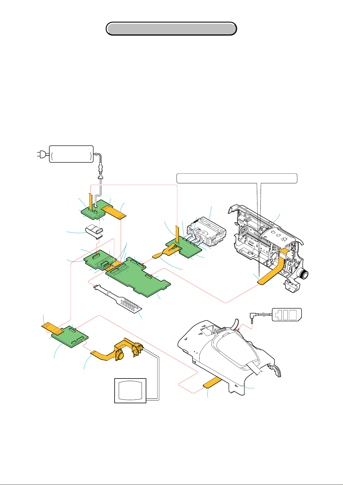
[SERVICE POSITION TO CHECK THE VTR SECTION]
Connection to Check the VTR Section
To check the VTR section, set the VTR to the "Forced VTR power ON" mode.
Power off the MIC PHANTOM switch.(Need to miniminze the power consumption as AC adapter capacity is limited.)
Operate the VTR functions using the adjustment remote commander
(with the HOLD switch set in the OFF position).
Note: This operation is not effected in the normal operation, and is effected only repairing.
Setting the “Forced VTR Power ON” mode
1) Select page: 0, address: 01, and set data: 01.
2) Select page: 0, address: 10, and set data: 00.
3) Select page: D, address: 23, set data: AF, and press
the PAUSE button of the adjustment remote commander.
Exiting the “Forced VTR Power ON” mode
1) Select page: 0, address: 01, and set data: 01.
2) Select page: 0, address: 10, and set data: 00.
3) Select page: D, address: 23, set data: FF, and press the
PAUSE button of the adjustment remote commander.
4) Select page: 0, address: 01, and set data: 00.
Mechanism deck
Cabinet (R) sectio
n
Cabinet (L) section
AC power adaptor
AC-L10A/L10B or
AC-L15A/L15B
AC IN
DC-IN
DC-IN jack
(To eject a cassette, connect the cabinet (R) assembly.)
DA-033
DB-018
Ver. 1.7 2007. 10
2-10
2. DISASSEMBLY
2. DISASSEMBLY
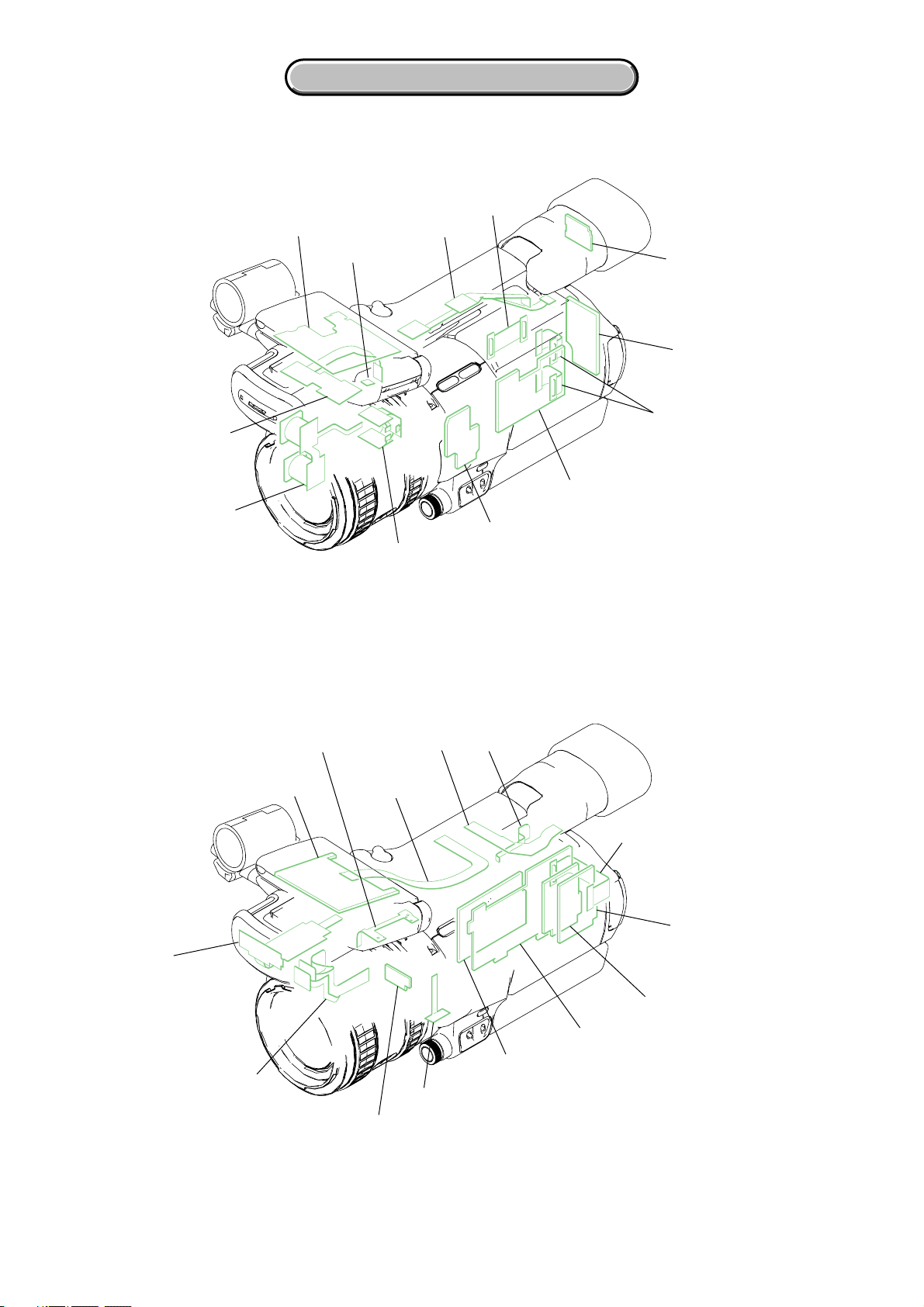
HVR-Z1J/Z1U/Z1N/Z1E/Z1P/Z1C
2-3. CIRCUIT BOARDS LOCATION
DB-018
VA-119
FP-959
DA-033
VC-367
FP-975
FP-967
FP-981
FP-964
FP-977
LB-106
MK-01
7
FK-090
SW-433
FP-980
FP-976
FP-971
PD-222
MA-431
MR-048
CK-143
CD-522
IF-122
JK-275
SE-150
FP-978
2-11
2. DISASSEMBLY
2. DISASSEMBLY
HVR-Z1J/Z1U/Z1N/Z1E/Z1P/Z1C
NAME
FUNCTION
R.G.B-CH CCD IMAGER, S/H, AGC
FUNCTION KEY
DC/DC CONVERTER
DC IN, CHARGE, DC/DC CONVERTER
VTR FUNCTION KEY
BATTERY
DV TERMINAL
MR SENSOR
RELAY
RELAY
RELAY
MIC TERMINAL
RELAY
RELAY
JACK
EVF BACK LIGHT
INT MIC AMP
FUNCTION KEY
REC/PB RF AMP, DRUM/CAPSTAN/LOADING MOTOR DRIVE
LCD DRIVER, TIMING GENERATOR
PITCH/YAM SENSOR AMP
PANEL REV
AUDIO IN /OUT, VIDEO IN/OUT, Y.PB.PR OUT AMP, XLR INPUT
CCD RF IN, R.G.B-CH AGC, A/D CONV, TIMING GENERATOR, CAMERA RGB PROCESS,
LENS DRIVE, LENS DRIVE CONTROL, CAMERA CONTROL, BASE BAND PROCESS,
OSD, D3 FILTER, HDV VIDEO ENCODER, 64MBIT SDRAM (L/U),
HDV SIGNAL/RF SIGNAL PROCESS, HDV VIDEO DECODER, 64MBIT Y/C-SDRAM,
ILINK, INTERFACE, DV/RF SIGNAL PROCESS, VIDEO A/D CONV., EVF RGB DRIVER,
TIMING GENERATOR, HDV AUDIO SIGNAL PROCESS, AUDIO INPUT SELECT,
AUDIO CONVERTER, D3 CONTROL, FRONT CONTROL, LSI CONTROL,
MECHA CONTROL, CONNECTOR-1, CONNECTOR-2
RELAY, REAR IR
CD-522
CK-143
DA-033
DB-018
FK-090
FP-959
MIC SELECTFP-960
FP-964
FP-967
FP-975
RELAYFP-977
FP-976
FP-978
FP-971
RELAYFP-972
RELAYFP-974
FP-980
FP-981
JK-275
IF-122
MA-431
VA-119
MR-048
SE-150
PD-222
SW-433
VC-367
LB-106
MK-017
2-12E
2. DISASSEMBLY
2. DISASSEMBLY
HVR-Z1J/Z1U/Z1N/Z1E/Z1P/Z1C
2-4. FLEXIBLE BOARDS LOCATION
The flexible boards contained in the mechanism deck and lens block are not shown.
FP-965
FP-972
FP-966
FP-985
FP-974
FP-984
FDM-009
CONTROL SWITCH BLOCK
(CF5610)
FP-962
FP-963
FP-961
FP-960
CONTROL SWITCH BLOCK
(PS5610)
CONTROL SWITCH BLOCK
(VV91010)
CONTROL SWITCH BLOCK
(ZS-5610)

HVR-Z1J/Z1U/Z1N/Z1E/Z1P/Z1C
Link
Link
3. BLOCK DIAGRAMS
POWER BLOCK DIAGRAM (1/4)
POWER BLOCK DIAGRAM (2/4)
POWER BLOCK DIAGRAM (3/4)
POWER BLOCK DIAGRAM (4/4)OVERALL BLOCK DIAGRAM (4/6)
OVERALL BLOCK DIAGRAM (5/6)
OVERALL BLOCK DIAGRAM (6/6)
OVERALL BLOCK DIAGRAM (3/6)
OVERALL BLOCK DIAGRAM (2/6)
OVERALL BLOCK DIAGRAM (1/6)
POWER BLOCK DIAGRAM (1/4)
POWER BLOCK DIAGRAM (2/4)
POWER BLOCK DIAGRAM (3/4)
POWER BLOCK DIAGRAM (4/4)OVERALL BLOCK DIAGRAM (4/6)
OVERALL BLOCK DIAGRAM (5/6)
OVERALL BLOCK DIAGRAM (6/6)
OVERALL BLOCK DIAGRAM (3/6)
OVERALL BLOCK DIAGRAM (2/6)
OVERALL BLOCK DIAGRAM (1/6)
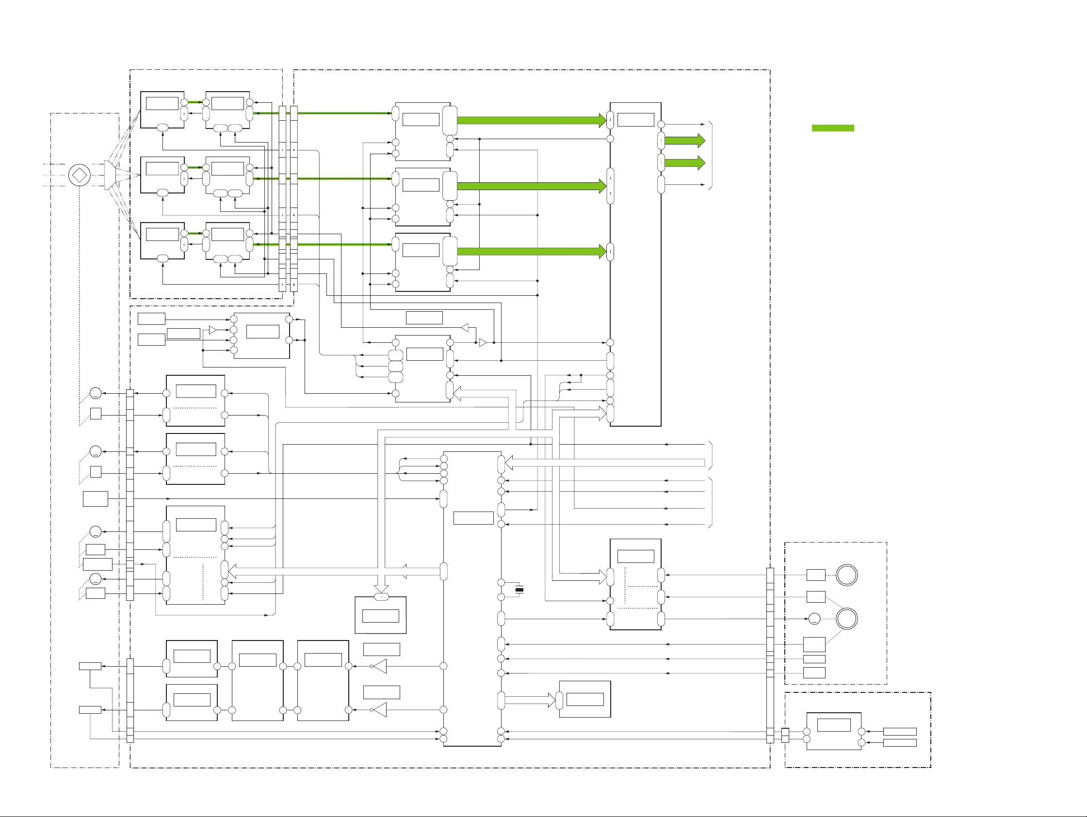
HVR-Z1J/Z1U/Z1N/Z1E/Z1P/Z1C
3-1 3-2
3-1. OVERALL BLOCK DIAGRAM (1/6)
3. BLOCK DIAGRAMS
( ) : Number in parenthesis ( ) indicates the division number of schematic diagram where the component is located.
V1R-V4R TG HD
TG VD
CD-522 BOARD VC-367 BOARD(1/6)
LENS BLOCK(2/2)
SE-150 BOARD
14
1
IC1504
M
3
IRIS DRIVE
IRIS PWM
OE1
OE2
A1
A2
B1
B2
CL IRIS PWM
CN1501
IRIS
METER
CL IRIS
METER
I DRIVE-
I HALL+
I HALL-
H
IRIS
DICHROIC
PRISM
IRIS
HALL AMP
I HALL AD
CL HALL AD
8
4-1
10
13
ZOOM
MOTOR
FOCUS
MOTOR
M
M
MR
R-CH
CCD IMAGER
PITCH
ACTIVE
LENS ACTUATOR
CN1503
16
YAW
EN1
DIR1A
DIR1B
SPCK
CAM DD ON
IC401
PITCH/YAW
SENSOR AMP
IC1104
B-CH
AGC
A/D CONV.
18
2
12
8
C1
A2 B1
C3
D1 D3
E1 E3
F1 F3
G1 G3
H1 J2
80.91908MHz
OSC
X1101
ND FILTER
SWITCH
ZOOM RESET
SENSOR
IC102
TO
OVERALL
BLOCK DIAGRAM
(2/6)
1
TO
OVERALL
BLOCK DIAGRAM
(6/6)
2
TO
OVERALL
BLOCK DIAGRAM
(5/6)
3
CCD OUT
RGR
H1R
H2R
F1
J4,G5
H1,J2
C1
B1
A8
J7
D9
E9
R-CH S/H
IC105
J8
BIL0-13
G5
J5
V1G-V4G TG HD
TG VD
SO GCAM
SCK GCAM
8
4-1
10
13
9
12
14
1
IC1505
M
3
CL IRIS DRIVE
CL DRIVE-
CL HALL+
CL HALL-
ND SW1
ND SW2
ND SW3
ZOOM A+
ZOOM A-
ZOOM B-
ZOOM B+
Z MR A
Z MR B
ZM RST SENS
FOCUS+
FOCUS-
F MR A
F MR B
H
CL IRIS
HALL AMP
9
12
K12
M9
J9
IC1702
ZOOM
MOTOR
DRIVE
FOCUS
MOTOR
DRIVE
F3
E3
B1
C4
K6
L4
F1
G3
E12
E10
L9
K9
6
IC1501
PITCH DRIVE
1
7
2
IC1502
YAW DRIVE
6
IC1503
PRE DRIVE
9
7
8
1
7
J11
K11
H12
L10
L11
G-CH
CCD IMAGER
IC103
CCD OUT
RGR
H1R
H2R
F1
J4,G5
H1,J2
C1
B1
A8
J7
D9
E9
G-CH S/H
IC106
V1B-V4B TG HD
TG VD
SO GCAM
SCK GCAM
SO GCAM
SCK GCAM
CDS+B
CDS-B
CDS+R
CDS-R
CDS+G
CDS-G
TG HD
TG VD
CHCK1
PBCLK
CHCK2
PBCLK
CLPOB
CLPOB
CLPOB
CHCK2
PBCLK
CHCK2
PBCLK
CN1001
8
4-1
10
13
B-CH
CCD IMAGER
IC101
CCD OUT
RGB
H1B
H2B
F1
J4,G5
H1,J2
C1
B1
F9
E9
A6
A5
IC1105
R-CH
AGC
A/D CONV.
J8
G5
J5
CAM HD
CAM VD
CAM FLD
SIRCKO
SO GCAM
SCK GCAM
SO GCAM
SCK GCAM
SO GCAM
SCK GCAM
V1B-V4B
V1R-V4R
V1G-V4G
TG HD
TG VD
TG FLD
CAM DD ON
PITCH PWM
42
F9
E9
A6
A5
IC1106
G-CH
AGC
A/D CONV.
J8
G5
J5
F9
E9
A6
A5
IC1101
TIMING
GENERATOR
IC1107
C4
B4 A5
B5
E1
F2 E2
E3
A7
B6 B7
A8
J5
CHCK1
71
3
2
5
4
G1
C8
J2
10
9
8
C2
A1
C1
A8
J7
D9
E9
B-CH S/H
IC104
9292
9090
7474
7171
42
40
42
40
6
4
52
6
4
52
62
61
62
61
63
64
63
64
26
23
26
23
7070
6767
81MHz
OSC
X1102
T END
W END
SENSOR
GM
SWITCH
GM PT
28
24
22
33
35
47
9
8
7
42
41
17
18
13
14
3
2
4
1
38
MR
3
1
95
96
135
139
128
98
142
94
IC1902
CAMERA
CONTROL
X1901
20MHz
73
71
66
65
63
69
70
67
176
175
41
77
78
75
210
211
6
7
5
4
9
2
RIL0-13
YO2-9
CO2-9
CLPOB
GIL0-13
ZM RST SENS
SPCK
EN1
DIR1A
DIR1B
C1
A2 B1
C3
D1 D3
E1 E3
F1 F3
G1 G3
H1 J2
C1
A2 B1
C3
D1 D3
E1 E3
F1 F3
G1 G3
H1 J2
I HALL AD
IRIS PWM
CL HALL AD
ND SW1
ND SW2
ND SW3
CL IRIS PWM
3
IC1506
IC1507
IC1508
LPF
IC1901
EEPROM
SO,SI,SCK
12
7
8
YAW PWM
42
131
132
129
130
67
CAM,SO,SI,SCK
CAM DD ON
ZOOM VR AD
138
306
192
169
310
IC1301
CAMERA
RGB
PROCESS
151
142
165
154
175
174
173
314
315
316
141
124
H ZOOM AD
ZOOM VR AD
H ZOOM AD
NTSC/XPAL DET
ZM SPD SEL
ZM SPD SEL
RNGMT EN
RNGMT PWM
136
49
184
91
SO GCAM
SCK GCAM
CAM,SO,SI,SCKCAM,SO,SI,SCK
103
95
68
62
41
22
K12
IC1701
FOCUS
RING MR
INPUT
ZOOM
RING MR
INPUT
ZOOM
RING
DRIVE
J11
K11
H12
L8
M8
L6
L7
E12
E10
B1
C4
CAM,SO,SI,SCK
HI,SO,SI,SCK HI,SO,SI,SCK
5
2
6
CAM,SO,SI,SCK
F RING MR A
F RING MR B
ZM RING MR A
ZM RING MR B
ZOOM RING+
ZOOM RING-
T END SENS
W END SENS
RING PTNS AD
GM SW
CN1502 CN401
SE401
SE402
SPCK
12
14
8
10
27
ZOOM
RING
MOTOR
FOCUS
RING
26
2
15
23
19
18
4
M
MR
MR
FOCUS
RING
4
2
LENS BLOCK
(1/2)
PITCH SENSOR
YAW SENSOR
CHCK
CHCK
CHCK
TG HD
CHCK2
TG VD
TG FLD
188
189
190
187
300
303
301
PITCH AD
YAW AD
PITCH POS AD
YAW POS AD
IC1903
EVR
CN101
(2/25) (3/25)
(2/25)
(2/25)
(2/25)
(2/25)
(4/25)
IC1102
(2/25)
2
3
5
7
1
IC1103
6
SELECTOR
(2/25)
(4/25)
(5/25)
(4/25)
(4/25) (4/25)
(4/25)
(4/25)
(6/25)
(6/25)
(6/25)
(5/25)
(4/25)
(PAGE 3-3)
(PAGE 3-12)
(PAGE 3-10)
VIDEO SIGNAL
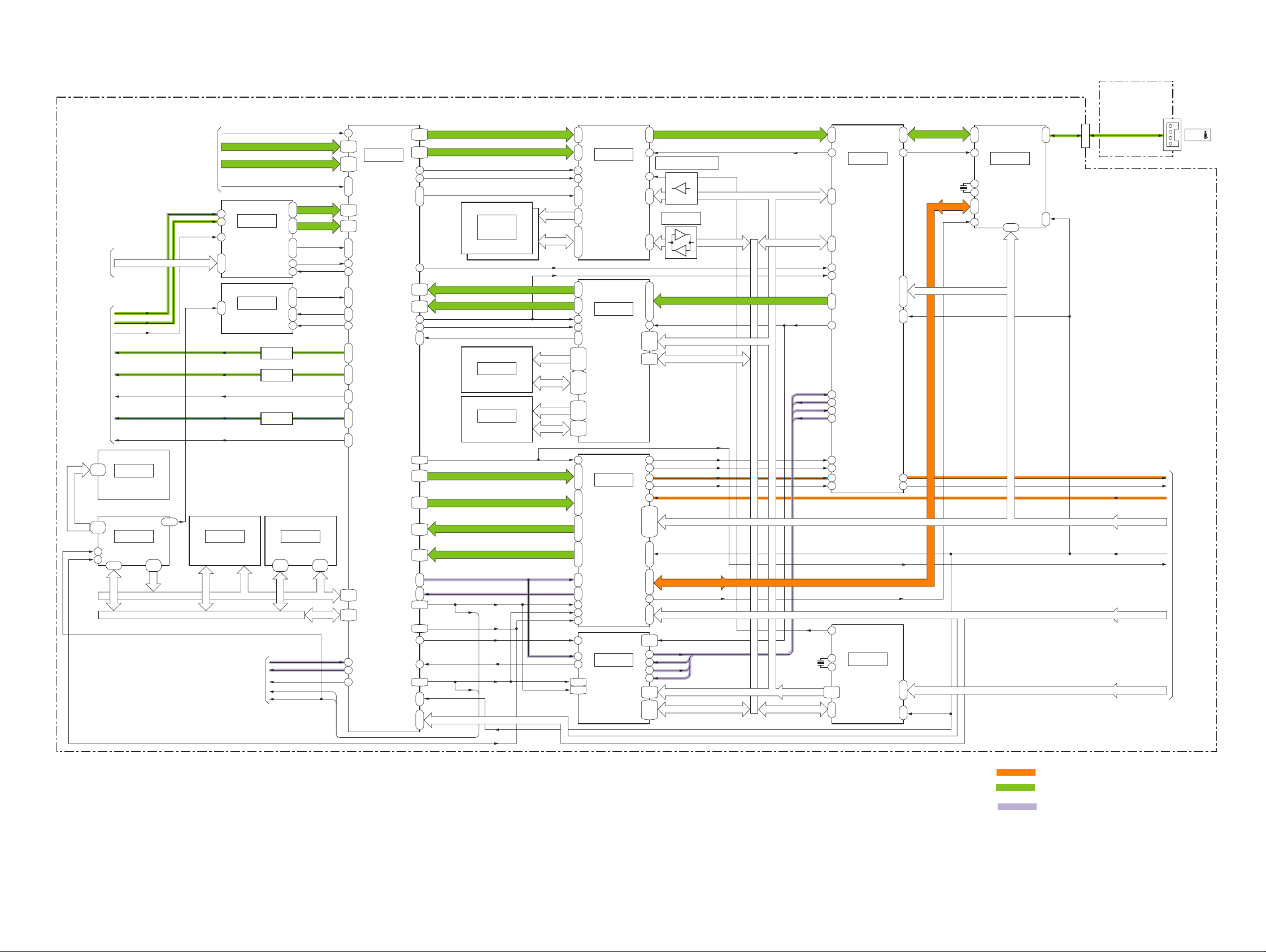
HVR-Z1J/Z1U/Z1N/Z1E/Z1P/Z1C
3-3 3-4
3-2. OVERALL BLOCK DIAGRAM (2/6)
( ) : Number in parenthesis ( ) indicates the division number of schematic diagram where the component is located.
CO0-CO7
RYO0-RYO3,DEHD,DEVD,DEFLD,SGOUT
RCO0-RCO3,EDHD,EDVD,EDFLD,FRMREF
RYI0-RYI3,DE0-DE3
RCI0-RCI3,DE4-DE7
IC2021
132
24
17
193
423
186
163
162
332
189
111
17
419
BASE BAND
PROCESS
135-140
361-366
26-29
264-267
30-38
273-276
222-234
442-452
8-15
245-252
130,133
134
355-360
169-172
395-398
164-167
390-393
107-110
339-342
55,54
102-105
334-338
45,46
283,285
43,44
281,282
53,290
291,292
51,52
288,289
161
•
382
•
386
174
•
399
•
173
257
•
258
•
19
262
•
25
•
263
315
•
85
•
317
115
•
344
418
•
197
419
•
201
254
255
A2-A19
D0-D15
SPCKO
CAM HD
CAM VD
CAM FLD
VFI HD
VFI VD
VFI OE
COLH1
COLH2
COLH3
AFCK
CK13MFO
CK14MFO
Y
PR
PB
Q2119-2121
Q2110-2112
HOSDHD
HOSDVD
YO2-YO9
YO0-YO9 EBS[0]-EBS[7]
CO2-CO9
VFIY0-VFIY7
VFIC0-VFIC7
IC5001
VIDEO
A/D
CONV.
IC2101
OSD
59
|
52
49
|
42
38
•
37
•
36
17
•
16
•
14
64
•
66
•
63
2
6
25
34
8
68
20
•
19
3
•
1
313
•
80
81
LPF
EVRE
EVGR
EVBL
XEHD
XEVD
XPHD
XPVD
Q2116-2118
BUFF
PLRE
PLGR
PLBL
YO
PRO
PBO
EVRE
EVGR
EVBL
XEHD
XEVD
XPHD
XPVD
PLRE
PLGR
PLBL
Q2113-2115
BUFF
75
•
79
•
77
73
•
72
•
74
68
•
69
•
67
297
•
65
64
•
56
IC8003
16Mbit
SDRAM
IC8001
FLASH
MEMORY
IC8009
DS
CONTROL
IC2208
HDV
VIDEO
ENCORDER
IC3001
HDV
VIDEO
DECORDER
IC4001
DV
SIGNAL
PROCESS
RF
SIGNAL
PROCESS
IC7001
HDV
AUDIO
SIGNAL
PROCESS
IC8601
LSI
CONTROL
IC2502
HDV
SIGNAL
PROCESS
HDV
RF SIGNAL
PROCESS
IC3501
iLINK
INTERFACE
59
|
52
8
|
16
78
|
86
241
|
251
297
|
304
187
|
197
77
|
85
139
|
136
95
|
98
242
|
246
251
|
259
18
|
26
154
|
173
1
60
75
241
226
291
252
143 86
30
45
41
71
72
276
279
277
281
73
74
80
82
20
1
3
139
104
59
35
60
47
21
97
45
74
78
15
CK56MF03
CK27MF0L
CK27MFO1
FLD27MFFLD27MF
CK27MFO1
CK DENEBO2
VCK
ADATAIN0
ADATAIN1
CK64FSO
CK13MFOCK13MFO
CKFSOCKFSO
CK64FSO
CKFSO
DSCK VM
ADATAOUT0
ADATAOUT1
DHD
DFD
HD
VD
FLD
3
•
2
•
4
A0-A10
A0-A10
D0-D63
D0-D31
A0-A10
D0-D31
IC2401
IC2402
64Mbit
SDRAM
IC3201
Y SDRAM
IC3202
C SDRAM
89
|
131
•
175
|
217
287
•
286
168
•
127
167
•
126
204
•
203
42,44
47-49
52-55
61,64
66
3-24
33-35
58,59
61
68-90
123-124
134-137
144-147
151
92-118
148,150
155-176
22,20
119
•
162
•
120
•
163
70
•
121
•
71
•
122
13
•
72
•
14
•
73
60
•
58
•
112
•
111
149
•
186
•
150
•
187
123
•
166
•
124
•
125
187,188
54
•
152
•
55
•
190
•
155
107
•
189
•
153
•
109
•
192
114
•
157
•
3
66
•
65
•
63
38,42
48,49
62,18
39,46
58,69
81,95
120,124
135,6
43,73
41,71
195,198
ADATAIN0
AUIN21 AUIN21
FRRV
TRRT
CK64FSO
DSCK VM
(1/2)
20-26
29-35
20-26
29-35
16-35
123
124
D0-D15
A1-A22
D0-D15 A1-A21
D0-D15 A1-A14
A1-A22
D0-D15
CKFSO
DSCK VM
AUIN1
ADAO1
CK64FSO
CKFSO
CK256FSO
TO
OVERALL
BLOCK DIAGRAM
(3/6)
6
Y
Y
C
C
CK
CK
TO
OVERALL
BLOCK DIAGRAM
(3/6)
5
TO
OVERALL
BLOCK DIAGRAM
(4/6)
4
TO
OVERALL
BLOCK DIAGRAM
(1/6)
1
VD SO,SI,SCK
KCLK KCLK
DJCLK
RF IN RF IN
SWP
FRRV
TRRT
TRRV
SWP
FRRV
TRRT
TRRV
DJCLK
VIT DT
VIT CK
CREC DT
CREC CK
VIT DT
VIT CK
CREC DT
CREC CK
MCLK
296 185 87
7
1
10
HDAT[0]-HDAT[7]
HDAT[0]-HDAT[7]
IC2301-2306
IC2206
215
225
223
221
220
231
227
224
191,218
193-201
204-207
210-213
179-189
192
AUDAL
AUDAO
AUENI
AUENO
AUDAO
AUENI
AUENO
AUDAL
MCLK
X8601
20MHz
HADR[0]-HADR[3] HADR[0]-HADR[7]
HADR[0]-HADR[3] HADR[0]-HADR[13]
44-37
33-28
HDAT[0]-HDAT[7] HDAT[0]-HDAT[7]
52
|
45
AUIN21
256
|
266
HDAT[0]-HDAT[7]
PD10-PD17
11
|
23
BS[0]-BS[7]
HADR[0]-HADR[13]
PCLK1
TRCK0
149
150
104
X3501
24.576MHz
235
229
204
|
207
213
|
224
FRRV
TRRT
REC DT
REC CK
REC DT
REC CK
LBUS0-LBUS3
LBUS0-LBUS3
TRCK0
100,102
291-304
1-32
103-105
235,236
51-64
MC BUS MC BUS
MC BUS
105
108
TPA
NTPA
TPB
NTPB
FRRV
TRRT
VCK
CN641
CN0009
FRRV
TRRT
FP-964
(FLEXIBLE
BOARD)
(1/2)
HDV/DV
TO
OVERALL
BLOCK DIAGRAM
(4/6)
7
VSP SO,SI,SCK
VSP2 SO,SI,SCK
VSP SO,SI,SCK
VSP2 SO,SI,SCK
5
•
6
•
4
•
3
VC-367 BOARD (2/6)
OSD SO
XOSD SCK
VY[0]-VY[7]
VC[0]-VC[7]
269
|
256
289
|
272
VSP SO,SI,SCK
16
(7/25)
(16/25)
(8/25)
(20/25)
IC8002
EEPROM
(20/25)
(20/25) (20/25)
(20/25)
(18/25)
(22/25)
(15/25)
(13/25)
(13/25)
(12/25)
(9/25)
(11/25)
(14/25)
(9/25)
(9/25)
(10/25)
1-3
5,6
(PAGE 3-2)
(PAGE 3-7)
(PAGE 3-5)
(PAGE 3-6)
(PAGE 3-7)
VIDEO/AUDIO SIGNAL
VIDEO SIGNAL
AUDIO SIGNAL
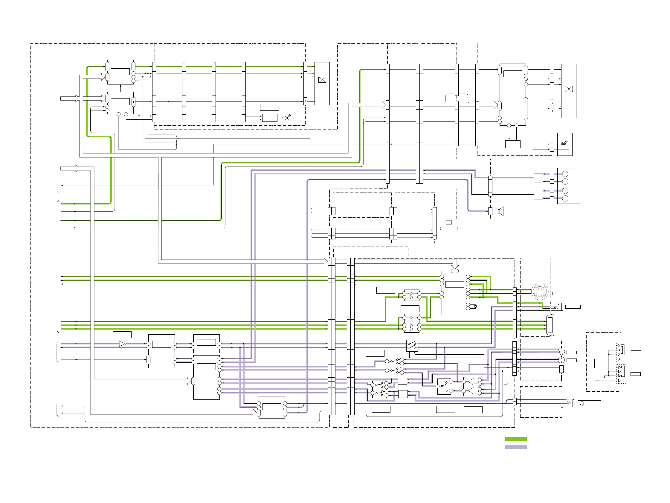
HVR-Z1J/Z1U/Z1N/Z1E/Z1P/Z1C
3-5 3-6
3-3. OVERALL BLOCK DIAGRAM (3/6)
( ) : Number in parenthesis ( ) indicates the division number of schematic diagram where the component is located.
VC-367 BOARD(3/6)
FP-975
(FLEXIBLE
BOARD)
(1/2)
EVRE
EVGR
EVBL
CN6001
CN802
CN501
CN800
12
27
35
48
47
46
20
22
24
40
39
RGB DRIVE
IC6001
IC501
CO2-9
XEHD
XEVD
EVF VG
EVF COM DC
PSIG
EXT DA
EVF VCO
1
48
2 8
46
45
42
23
13
TIMING
GENERATOR
IC6002
BL CONT
EVRE
EVGR
EVBL
PLRE
PLGR
PLBL
XEHD
XEVD
8
7
9
6
31
11
19
30
28
29
33
34
32
35
9
10
30
22
10
13
12
FP-980
(FLEXIBLE
BOARD)
(1/2)
FP-981
(FLEXIBLE
BOARD)
(1/2)
FP-976 (1)
(FLEXIBLE BOARD)(1/3)
FP-976 (2)
(FLEXIBLE BOARD)(1/4)
FP-971(FLEXIBLE BOARD)(1/2)
FP-978
(FLEXIBLE BOARD)
FP-960
(FLEXIBLE BOARD)
DA-033 BOARD
(1/3)
JK-275
BOARD
IF-122 BOARD
(1/2)
PD-222 BOARD
BACK
LIGHT
MA-431 BOARD(1/2)
23
24
22
25
1
20
12
1
5
4
FP-984
(FLEXIBLE
BOARD)
LB-106 BOARD
11
10
12
9
33
14
22
32
29
30
LED DA
HST,HCK1,HCK2,RGT,DWN,EN,STB,VCK,VST,PCG
PSIG
COM
R,G,B
D501
BACK
LIGHT
XPHD
XPVD
A INT MIC1
CN2004
CN710CN711
CN0003
CN760
CN760
CN0005
CN0002
EVF VG
CPC
CN107
FOR
ADJUSTMENTS
PSIG
EXT DA
EVF VCO
A INT MIC2
SP+,SP-
LED ON/OFF
CN502
15
16
14
17
18
12
3
BACK LIGHT
DRIVE
Q501,502
BACK LIGHT
DRIVE
MIX
AMP
PLRE
PLGR
PLBL
CN0008 CN306
CN308
CN305
CN811
COLOR
EVF
UNIT
LCD902
COLOR
LCD UNIT
LCD901
LED901
MIC901
MIC UNIT
TO
OVERALL
BLOCK DIAGRAM
(4/6)
8
TO
OVERALL
BLOCK DIAGRAM
(5/6)
9
TO
OVERALL
BLOCK DIAGRAM
(2/6)
5
XPHD
XPVD
Y
C
CK
YO
16
PRO
PBO
ADAO1
AUIN11
CH1_48V_ON
CH2_48V_ON
CKFSO
CK64FSO
CK256FSO
VD SO,SCKVD SO,SI,SCK
VD SO,SI,SCK
3
2
1
11
12
9
14
13
15
38
36
35
34
38
39
40
30
29
32
27
28
26
3
2
1
9
1
SCK
VD SO,SI
PANELHD
PANEL R,G,B
PANELVD
BL CONT
2
4
3
5
3
2
1
11
9
12
14
13
15
4
5
3
23
1
6
2
4
5
6
38
39
40
30
29
32
27
28
26
2
4
5
6
51
55
13
51
51
55
49
51
55
13
51
49
1
18
2
17
16
27
26
23
13
51
49
CN101
CN103
11
9
1
7
5
EVF COM DC
Y
C
Y
C
Y
C
SY
SC
Y
PR
PB
VIDEO I/O
AU LINE I/O L
AU LINE I/O R
XLR-1+
XLR-2+
XLR-1-
XLR-2-
CH1 48V ON
CH2 48V ON
HP_AU_L
HP_AU_R
1
5
3
L
V
R
Y
C
V
V
CK
YO
PRO
PBO
A AV OUT L
Q2010,2011
A AV OUT R
EXT MIC L+
EXT MIC R+
EXT MIC L-
EXT MIC R-
23
25
43
42
31 28
40
39
38
48
47
46
19
20
21
35
2
4
14
15
32
RGB DRIVE
VR,VG,VB
TIMING
GENERATOR
IC601
COM
PSIG
18
36
34
26
39
48
42
14
22
28
30
46
7
5
10
7
14
910
VIDEO
IN/OUT
AGC
ACC
X2201
13.5MHz
IC2201
IC2301
IC2302
IC2003
VD SO,SI,SCK
EXTDA
CN601
Q601-604
Q104,106,110
Q105,107,111
BL ON
BL ANODE
BL CATHODE
CN603
CN604
CN101
CN303
CN304
CN102
BL LO
22
19
13
7
2
3
1
3 FRONT
REAR
MIC
L
2
9
7
1
SP901
SPEAKER
2
MIC
L
MIX
AMP
2 FRONT
REAR
MIC
R
3
MIC
R
VD SO,SCKVD SO,SCK
14
13
3
12 14
10
5
8
7
1
18
2
17
16
27
26
75
73
23
75
73
98
97
83
82
86
84
1
18
2
17
16
27
26
75
73
23
98
97
83
82
86
84
19
21
15
4
2
6
13
17
4
12
5
Q2407,2411,2419
Q2409,2413,2421
Q2408,2412,2420
Q2410,2414,2422
AMP
EXT
MIC
AMP
EXT
MIC
CN2006
CN2005
CN783
CN2007
S VIDEO
J102
INPUT2
CN782
INPUT1
CN781
CH 2
S602
CH 1
S601
COMPONENT
OUTPUT
CN101
AUDIO VIDEO
J103
YC
G
G
CONTROLSWICH BLOCK
(PS5610)(1/2)
(HEADPHONES)
J102
4
1
15
17
D6
B6
D2
B2
B4
A5
E1
E5
SPEAKER AMP
HP CH1
HP CH2
SP+
SP-
HEADPHONE AMP
IC7120
7
1
6
2
LINE OUT
GAINUP
IC7113
26
27
5
3
13
14
AUDIO
A/D CONV.
D/A CONV.
IC7115
IC7119
6
11
3
8
4
9
5
10
41
39
AUDIO INPUT
SELECT
A INT MIC 1
A INT MIC 2
CH1
CH2
A AV OUT L
A AV OUT R
A LINE L
A LINE R
EXT MIC L+
EXT MIC R+
EXT MIC L-
EXT MIC R-
IC7114
30
29
15
12
11
CH1
CH2
4
2
TO
OVERALL
BLOCK DIAGRAM
(2/6)
6
VSP SO,SCK
VSP SO,SCK
VSP SO,SCK
VA-119 BOARD(1/2)
97
98
82
83
84
86
1
18
2
17
16
27
26
23
75
73
91
90
91
90
91
90
91
90
97
98
82
83
84
86
85
87
85
87
85
87
85
87
(17/25)
(19/25)
(19/25)
(19/25)
(19/25)
(19/25)
(17/25)
(PAGE 3-7)
(PAGE 3-10)
(PAGE 3-3)
(PAGE 3-3)
TO
OVERALL
BLOCK DIAGRAM
(4/6)
qd
(PAGE 3-7)
(3/4)
(3/4)
(1/4)
IC2043
(4/4)
IC2044
(4/4)
IC2405
(4/4)
(2/4)
14
12
13
4
5
3
1
+
–
2
7
5
6
1
7
6
VIDEO SIGNAL
AUDIO SIGNAL
A LINE L
A LINE R
CN761
CN761
51
55
13
51
49
10
9
7
3
4
2
1
6
3
+
–
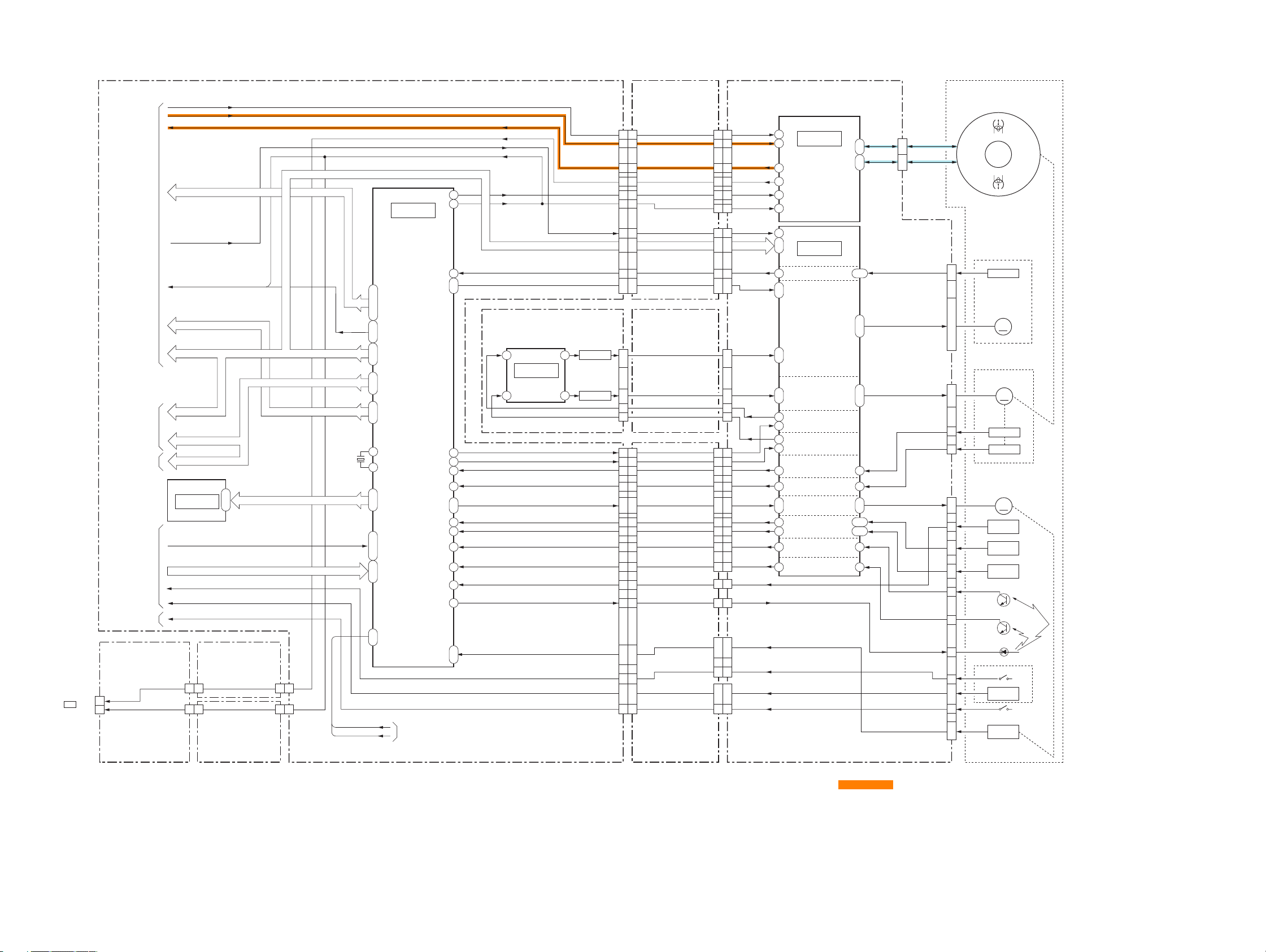
HVR-Z1J/Z1U/Z1N/Z1E/Z1P/Z1C
3-7 3-8
3-4. OVERALL BLOCK DIAGRAM (4/6)
( ) : Number in parenthesis ( ) indicates the division number of schematic diagram where the component is located.
VSP2 SO,SI,SCK
MC BUS
RF IN
REC DT
REC CK
SWP,FRRV,TRRT,TRRV
VCK
VSP SO,SCK
VSP SO,SCK
IC8801
MECHA
CONTROL
(23/25)
172
164
190
89
88
197
198
192
193
196
195
119
180
165
•
166
CAP FG
CONT1
SWP
CAP ON,CAP FWD
CAP FG
CAP ON
CAP FWD
CAP PWM
DRUM PWM
DRUM FG
DRUM PG
LOAD,UNLOAD
T REEL FG
S REEL FG
TAAPE END
TAPE TOP
DEW DET
TAPE LED ON
MODE SW A-MODE SW C
CH1_48V_ON
CH2_48V_ON
IC0101
REC/PB
AMP
(1/2)
IC201
CAPSTAN
FG AMP
CAPSTAN
MOTOR
DRIVE
DRUM
MOTOR
DRIVE
CAP
PWM
LPF
DRUM
PWM
LPF
DRUM
FG
AMP
DRUM
PG
AMP
LOADING
MOTOR
DRIVE
REEL
FG
AMP
TAPE
END
DETECT
(2/2)
44
46
35
30
39
38
35
4
43
41
45
44
53
50
29
25
52
49
21 20
TAPE
TOP
DETECT
19 18
REC CK
REC DT
RF IN
ODD
EVEN
FG 1,2
CAP U,V,W
RF MON
CONT1
SWP
VCK
CAP VS
DRUM VS
55
22
13 13
15 15
99
10 10
18 18
30
•
29
30
•
29
14
•
16
14
•
16
28 28
38
•
36
10
•
9
4
•
3
80
•
1
75
•
77
64
•
67
32
•
33
22
•
21
22
•
21
69
•
72
IC201
PWM
DRIVE
(2/2)
(1/2)
H6
J6
G11
G8
SWITCHING
SWITCHING
CAP ERROR
DRUM ERROR
Q218
Q219
14
|
12
11
•
10
16
15
15
|
17
18
•
19
13
14
DB-018 BOARD (1/2)
FP-974
(FLEXIBLE
BOARD)(1/2)
FP-974
(FLEXIBLE
BOARD)(2/2)
FP-976 (2)
(FLEXIBLE
BOARD)(2/4)
CN206
CN0007 CN742 CN740
CN741
CN741CN742
CN0007
CN0101
CN103
CN740 CN102
CN741
CN741
CN103
CN740 CN102
CN103
CN103
CN102
FP-985
(FLEXIBLE
BOARD)
12 12
10 10
77
88
63
•
65
•
68
74
•
76
•
78
26•27
7•8
22•23
24 24
25 25
26 26
27 27
9
•
10
19
21
24
23
7
6
5
4
9
•
10
19
21
24
23
7
6
5
4
27 27
31 31
36 36
26 26
Z MECHA DECK
(MDX-Z311)
DRUM
M
MR-048 BOARD
6
•
5
9
•
8
CN104
CN203
M903
CN201
CN202
DRUM U,V,W
LM +,–
T REEL +,–
S REEL +,–
DEW AD
XCC DOWN
22
•
25
5
|
10
1
|
4
13
|
15
20
|
17
•
4
|
1
•
11
|
14
1
5
20
2
CAPSTAN FG
DRUM FG
DRUM FG
DEW
SENSOR
T REEL
SENSOR
S REEL
SENSOR
Q901
TAPE END SENSOR
M901
CAPSTAN
MOTOR
M
DRUM
MOTOR
M
M902
LOADING
MOTOR
26
•
25
11
18
Q902
TAPE TOP SENSOR
D901
TAAPE LED
MIC902
S903
S902
REC PROOF
7
|
9
12
17
22
•
23
H902
H901
MODE
SWITCH
C. C. DOWN
4PIN
CONNECTOR
30
|
28
30
|
28
34
|
32
34
|
32
17 17
55
22 22
19
|
21
19
|
21
44
1
|
3
1
|
3
15
•
13
106
|
108
63
•
65
•
68
54
•
55
86
•
87
•
84
117
•
178
•
179
69
•
70
•
67
82
•
83
•
80
73
•
74
•
71
113
•
114
•
56
•
57
52
|
45
33
|
30
1
3
X8801
20MHz
FP-976 (1)
(FLEXIBLE
BOARD)(3/4)
53
53
53
53
53
53
53
5315
13
DA-033 BOARD
(2/3)
HI SO,SI,SCK
CHIME SDA,CHIME SCK,CHIME VDD
REC PROOF
XCC DOWN
REC LEVEL VOL CH1
REC LEVEL VOL CH2
MANUAL REC CH1
MANUAL REC CH2
EEP SO,SI,SCK
IC8802
EEPROM
(23/25)
5
•
2
•
6
VD SO,SCK
VD SO,SI,SCK
VD SO,SI,SCK
VC-367 BOARD (4/6)
VSP SO,SI,SCK
48 48
51 51
40 40
38 38
44 44
43 43
13 18
1
•
2
1
•
21
17
•
15
17
•
15
33
RF MON
SWP
CN101 CN0003
CN0005
CN760CN761
CN761
CN760
CN103
16
CN107
(FOR ADJUSTMENT)
CPC
TO
OVERALL
BLOCK DIAGRAM
(5/6)
qa
TO
OVERALL
BLOCK DIAGRAM
(6/6)
q;
TO
OVERALL
BLOCK DIAGRAM
(2/6)
4
TO
OVERALL
BLOCK DIAGRAM
(3/6)
8
TO
OVERALL
BLOCK DIAGRAM
(2/6)
7
SWP
FRRV
TRRT
TRRV
(PAGE 3-4)
(PAGE 3-5)
(PAGE 3-3)
(PAGE 3-10)
TO
OVERALL
BLOCK DIAGRAM
(3/8)
(PAGE 3-5)
(PAGE 3-12)
VIDEO/AUDIO SIGNAL
qd
Loading...