


LAN8720/LAN8720i
Small Footprint RMII 10/100
Ethernet Transceiver with HP
Auto-MDIX Support
PRODUCT FEATURES |
Datasheet |
Highlights
Single-Chip Ethernet Physical Layer Transceiver (PHY)
Comprehensive flexPWR® Technology
—Flexible Power Management Architecture
—Power savings of up to 40% compared to competition
—LVCMOS Variable I/O voltage range: +1.6V to +3.6V
—Integrated 1.2V regulator
HP Auto-MDIX support
Miniature 24 pin QFN lead-free RoHS compliant package (4 x 4 x 0.85mm height).
Target Applications
Set-Top Boxes
Networked Printers and Servers
Test Instrumentation
LAN on Motherboard
Embedded Telecom Applications
Video Record/Playback Systems
Cable Modems/Routers
DSL Modems/Routers
Digital Video Recorders
IP and Video Phones
Wireless Access Points
Digital Televisions
Digital Media Adaptors/Servers
Gaming Consoles
POE Applications
Key Benefits
High-Performance 10/100 Ethernet Transceiver
—Compliant with IEEE802.3/802.3u (Fast Ethernet)
—Compliant with ISO 802-3/IEEE 802.3 (10BASE-T)
—Loop-back modes
—Auto-negotiation
—Automatic polarity detection and correction
—Link status change wake-up detection
—Vendor specific register functions
Power and I/Os
—Various low power modes
—Integrated power-on reset circuit
—Two status LED outputs
—Latch-Up Performance Exceeds 150mA per EIA/JESD 78, Class II
—May be used with a single 3.3V supply
Advanced Features
—Able to use a low cost 25Mhz crystal for the lowest eBOM
Packaging
—24-pin QFN (4x4 mm) Lead-Free RoHS Compliant package with RMII
Environmental
—Extended Commercial Temperature Range (0°C to +85°C)
—Industrial Temperature Range (-40°C to +85°C) version available (LAN8720i)
SMSC LAN8720/LAN8720i
DATASHEET
Revision 1.0 (05-28-09)

Small Footprint RMII 10/100 Ethernet Transceiver with HP Auto-MDIX Support
Datasheet
ORDER NUMBER(S):
LAN8720A-CP-TR FOR 24-PIN, QFN LEAD-FREE ROHS COMPLIANT PACKAGE (0 TO +85°C TEMP) LAN8720Ai-CP-TR FOR 24-PIN, QFN LEAD-FREE ROHS COMPLIANT PACKAGE (-40 TO +85°C TEMP)
Reel Size is 4000
80 ARKAY DRIVE, HAUPPAUGE, NY 11788 (631) 435-6000, FAX (631) 273-3123
Copyright © 2009 SMSC or its subsidiaries. All rights reserved.
Circuit diagrams and other information relating to SMSC products are included as a means of illustrating typical applications. Consequently, complete information sufficient for construction purposes is not necessarily given. Although the information has been checked and is believed to be accurate, no responsibility is assumed for inaccuracies. SMSC reserves the right to make changes to specifications and product descriptions at any time without notice. Contact your local SMSC sales office to obtain the latest specifications before placing your product order. The provision of this information does not convey to the purchaser of the described semiconductor devices any licenses under any patent rights or other intellectual property rights of SMSC or others. All sales are expressly conditional on your agreement to the terms and conditions of the most recently dated version of SMSC's standard Terms of Sale Agreement dated before the date of your order (the "Terms of Sale Agreement"). The product may contain design defects or errors known as anomalies which may cause the product's functions to deviate from published specifications. Anomaly sheets are available upon request. SMSC products are not designed, intended, authorized or warranted for use in any life support or other application where product failure could cause or contribute to personal injury or severe property damage. Any and all such uses without prior written approval of an Officer of SMSC and further testing and/or modification will be fully at the risk of the customer. Copies of this document or other SMSC literature, as well as the Terms of Sale Agreement, may be obtained by visiting SMSC’s website at http://www.smsc.com. SMSC is a registered trademark of Standard Microsystems Corporation (“SMSC”). Product names and company names are the trademarks of their respective holders.
SMSC DISCLAIMS AND EXCLUDES ANY AND ALL WARRANTIES, INCLUDING WITHOUT LIMITATION ANY AND ALL IMPLIED WARRANTIES OF MERCHANTABILITY, FITNESS FOR A PARTICULAR PURPOSE, TITLE, AND AGAINST INFRINGEMENT AND THE LIKE, AND ANY AND ALL WARRANTIES ARISING FROM ANY COURSE OF DEALING OR USAGE OF TRADE. IN NO EVENT SHALL SMSC BE LIABLE FOR ANY DIRECT, INCIDENTAL, INDIRECT, SPECIAL, PUNITIVE, OR CONSEQUENTIAL DAMAGES; OR FOR LOST DATA, PROFITS, SAVINGS OR REVENUES OF ANY KIND; REGARDLESS OF THE FORM OF ACTION, WHETHER BASED ON CONTRACT; TORT; NEGLIGENCE OF SMSC OR OTHERS; STRICT LIABILITY; BREACH OF WARRANTY; OR OTHERWISE; WHETHER OR NOT ANY REMEDY OF BUYER IS HELD TO HAVE FAILED OF ITS ESSENTIAL PURPOSE, AND WHETHER OR NOT SMSC HAS BEEN ADVISED OF THE POSSIBILITY OF SUCH DAMAGES.
Revision 1.0 (05-28-09) |
2 |
SMSC LAN8720/LAN8720i |
|
DATASHEET |
|

Small Footprint RMII 10/100 Ethernet Transceiver with HP Auto-MDIX Support
Datasheet
Table of Contents
Chapter 1 Introduction . . . . . . . . . . . . . . . . . . . . . . . . . . . . . . . . . . . . . . . . . . . . . . . . . . . . . . . 9
1.1 General Terms and Conventions . . . . . . . . . . . . . . . . . . . . . . . . . . . . . . . . . . . . . . . . . . . . . . . . . . . 9
1.2 General Description . . . . . . . . . . . . . . . . . . . . . . . . . . . . . . . . . . . . . . . . . . . . . . . . . . . . . . . . . . . . . 9
1.3 Architectural Overview . . . . . . . . . . . . . . . . . . . . . . . . . . . . . . . . . . . . . . . . . . . . . . . . . . . . . . . . . . 10
1.3.1 Configuration . . . . . . . . . . . . . . . . . . . . . . . . . . . . . . . . . . . . . . . . . . . . . . . . . . . . . . . . . . 10
Chapter 2 Pin Configuration . . . . . . . . . . . . . . . . . . . . . . . . . . . . . . . . . . . . . . . . . . . . . . . . . 12
2.1 Package Pin-out Diagram and Signal Table. . . . . . . . . . . . . . . . . . . . . . . . . . . . . . . . . . . . . . . . . . 12
Chapter 3 Pin Description. . . . . . . . . . . . . . . . . . . . . . . . . . . . . . . . . . . . . . . . . . . . . . . . . . . . 14
3.1 MAC Interface Signals . . . . . . . . . . . . . . . . . . . . . . . . . . . . . . . . . . . . . . . . . . . . . . . . . . . . . . . . . . 15
3.2 LED Signals . . . . . . . . . . . . . . . . . . . . . . . . . . . . . . . . . . . . . . . . . . . . . . . . . . . . . . . . . . . . . . . . . . 15
3.3 Management Signals . . . . . . . . . . . . . . . . . . . . . . . . . . . . . . . . . . . . . . . . . . . . . . . . . . . . . . . . . . . 16
3.4 General Signals . . . . . . . . . . . . . . . . . . . . . . . . . . . . . . . . . . . . . . . . . . . . . . . . . . . . . . . . . . . . . . . 16
3.5 10/100 Line Interface Signals . . . . . . . . . . . . . . . . . . . . . . . . . . . . . . . . . . . . . . . . . . . . . . . . . . . . . 17
3.6 Analog Reference . . . . . . . . . . . . . . . . . . . . . . . . . . . . . . . . . . . . . . . . . . . . . . . . . . . . . . . . . . . . . . 17
3.7 Power Signals. . . . . . . . . . . . . . . . . . . . . . . . . . . . . . . . . . . . . . . . . . . . . . . . . . . . . . . . . . . . . . . . . 17
Chapter 4 Architecture Details. . . . . . . . . . . . . . . . . . . . . . . . . . . . . . . . . . . . . . . . . . . . . . . . 18
4.1 Top Level Functional Architecture . . . . . . . . . . . . . . . . . . . . . . . . . . . . . . . . . . . . . . . . . . . . . . . . . 18 4.2 100Base-TX Transmit. . . . . . . . . . . . . . . . . . . . . . . . . . . . . . . . . . . . . . . . . . . . . . . . . . . . . . . . . . . 18 4.2.1 100M Transmit Data Across the MII/RMII Interface. . . . . . . . . . . . . . . . . . . . . . . . . . . . . 18 4.2.2 4B/5B Encoding. . . . . . . . . . . . . . . . . . . . . . . . . . . . . . . . . . . . . . . . . . . . . . . . . . . . . . . . 19 4.2.3 Scrambling. . . . . . . . . . . . . . . . . . . . . . . . . . . . . . . . . . . . . . . . . . . . . . . . . . . . . . . . . . . . 20 4.2.4 NRZI and MLT3 Encoding . . . . . . . . . . . . . . . . . . . . . . . . . . . . . . . . . . . . . . . . . . . . . . . . 20 4.2.5 100M Transmit Driver . . . . . . . . . . . . . . . . . . . . . . . . . . . . . . . . . . . . . . . . . . . . . . . . . . . 20 4.2.6 100M Phase Lock Loop (PLL) . . . . . . . . . . . . . . . . . . . . . . . . . . . . . . . . . . . . . . . . . . . . . 21
4.3 100Base-TX Receive . . . . . . . . . . . . . . . . . . . . . . . . . . . . . . . . . . . . . . . . . . . . . . . . . . . . . . . . . . . 21 4.3.1 100M Receive Input. . . . . . . . . . . . . . . . . . . . . . . . . . . . . . . . . . . . . . . . . . . . . . . . . . . . . 21 4.3.2 Equalizer, Baseline Wander Correction and Clock and Data Recovery . . . . . . . . . . . . . 21 4.3.3 NRZI and MLT-3 Decoding . . . . . . . . . . . . . . . . . . . . . . . . . . . . . . . . . . . . . . . . . . . . . . . 22 4.3.4 Descrambling. . . . . . . . . . . . . . . . . . . . . . . . . . . . . . . . . . . . . . . . . . . . . . . . . . . . . . . . . . 22 4.3.5 Alignment. . . . . . . . . . . . . . . . . . . . . . . . . . . . . . . . . . . . . . . . . . . . . . . . . . . . . . . . . . . . . 22 4.3.6 5B/4B Decoding. . . . . . . . . . . . . . . . . . . . . . . . . . . . . . . . . . . . . . . . . . . . . . . . . . . . . . . . 22 4.3.7 Receive Data Valid Signal . . . . . . . . . . . . . . . . . . . . . . . . . . . . . . . . . . . . . . . . . . . . . . . . 22 4.3.8 Receiver Errors . . . . . . . . . . . . . . . . . . . . . . . . . . . . . . . . . . . . . . . . . . . . . . . . . . . . . . . . 23 4.3.9 100M Receive Data Across the MII/RMII Interface . . . . . . . . . . . . . . . . . . . . . . . . . . . . . 23
4.4 10Base-T Transmit . . . . . . . . . . . . . . . . . . . . . . . . . . . . . . . . . . . . . . . . . . . . . . . . . . . . . . . . . . . . . 23 4.4.1 10M Transmit Data Across the MII/RMII Interface. . . . . . . . . . . . . . . . . . . . . . . . . . . . . . 23 4.4.2 Manchester Encoding . . . . . . . . . . . . . . . . . . . . . . . . . . . . . . . . . . . . . . . . . . . . . . . . . . . 24 4.4.3 10M Transmit Drivers . . . . . . . . . . . . . . . . . . . . . . . . . . . . . . . . . . . . . . . . . . . . . . . . . . . 24
4.5 10Base-T Receive . . . . . . . . . . . . . . . . . . . . . . . . . . . . . . . . . . . . . . . . . . . . . . . . . . . . . . . . . . . . . 24 4.5.1 10M Receive Input and Squelch . . . . . . . . . . . . . . . . . . . . . . . . . . . . . . . . . . . . . . . . . . . 24 4.5.2 Manchester Decoding . . . . . . . . . . . . . . . . . . . . . . . . . . . . . . . . . . . . . . . . . . . . . . . . . . . 24 4.5.3 10M Receive Data Across the MII/RMII Interface . . . . . . . . . . . . . . . . . . . . . . . . . . . . . . 25 4.5.4 Jabber Detection . . . . . . . . . . . . . . . . . . . . . . . . . . . . . . . . . . . . . . . . . . . . . . . . . . . . . . . 25
4.6 MAC Interface. . . . . . . . . . . . . . . . . . . . . . . . . . . . . . . . . . . . . . . . . . . . . . . . . . . . . . . . . . . . . . . . . 25 4.6.1 RMII . . . . . . . . . . . . . . . . . . . . . . . . . . . . . . . . . . . . . . . . . . . . . . . . . . . . . . . . . . . . . . . . . 25 4.7 Reference Clock . . . . . . . . . . . . . . . . . . . . . . . . . . . . . . . . . . . . . . . . . . . . . . . . . . . . . . . . . . . . . . . 26 4.7.1 REF_CLK In Mode . . . . . . . . . . . . . . . . . . . . . . . . . . . . . . . . . . . . . . . . . . . . . . . . . . . . . 27 4.7.2 REF_CLK OUT Mode . . . . . . . . . . . . . . . . . . . . . . . . . . . . . . . . . . . . . . . . . . . . . . . . . . . 27
SMSC LAN8720/LAN8720i |
3 |
Revision 1.0 (05-28-09) |
|
DATASHEET |
|

Small Footprint RMII 10/100 Ethernet Transceiver with HP Auto-MDIX Support
Datasheet
4.8 Auto-negotiation . . . . . . . . . . . . . . . . . . . . . . . . . . . . . . . . . . . . . . . . . . . . . . . . . . . . . . . . . . . . . . . 29 4.8.1 Parallel Detection . . . . . . . . . . . . . . . . . . . . . . . . . . . . . . . . . . . . . . . . . . . . . . . . . . . . . . 31 4.8.2 Re-starting Auto-negotiation . . . . . . . . . . . . . . . . . . . . . . . . . . . . . . . . . . . . . . . . . . . . . . 31 4.8.3 Disabling Auto-negotiation. . . . . . . . . . . . . . . . . . . . . . . . . . . . . . . . . . . . . . . . . . . . . . . . 31 4.8.4 Half vs. Full Duplex . . . . . . . . . . . . . . . . . . . . . . . . . . . . . . . . . . . . . . . . . . . . . . . . . . . . . 31
4.9 HP Auto-MDIX Support. . . . . . . . . . . . . . . . . . . . . . . . . . . . . . . . . . . . . . . . . . . . . . . . . . . . . . . . . . 31 4.10 nINTSEL Strapping and LED Polarity Selection . . . . . . . . . . . . . . . . . . . . . . . . . . . . . . . . . . . . . . . 32 4.11 REGOFF and LED Polarity Selection . . . . . . . . . . . . . . . . . . . . . . . . . . . . . . . . . . . . . . . . . . . . . . . 33 4.12 PHY Address Strapping . . . . . . . . . . . . . . . . . . . . . . . . . . . . . . . . . . . . . . . . . . . . . . . . . . . . . . . . . 34 4.13 Variable Voltage I/O . . . . . . . . . . . . . . . . . . . . . . . . . . . . . . . . . . . . . . . . . . . . . . . . . . . . . . . . . . . . 34 4.14 Transceiver Management Control . . . . . . . . . . . . . . . . . . . . . . . . . . . . . . . . . . . . . . . . . . . . . . . . . 34
4.14.1 Serial Management Interface (SMI). . . . . . . . . . . . . . . . . . . . . . . . . . . . . . . . . . . . . . . . . 34
Chapter 5 SMI Register Mapping . . . . . . . . . . . . . . . . . . . . . . . . . . . . . . . . . . . . . . . . . . . . . 36
5.1 SMI Register Format. . . . . . . . . . . . . . . . . . . . . . . . . . . . . . . . . . . . . . . . . . . . . . . . . . . . . . . . . . . . 40 5.2 Interrupt Management . . . . . . . . . . . . . . . . . . . . . . . . . . . . . . . . . . . . . . . . . . . . . . . . . . . . . . . . . . 48 5.2.1 Primary Interrupt System. . . . . . . . . . . . . . . . . . . . . . . . . . . . . . . . . . . . . . . . . . . . . . . . . 48 5.2.2 Alternate Interrupt System. . . . . . . . . . . . . . . . . . . . . . . . . . . . . . . . . . . . . . . . . . . . . . . . 49
5.3 Miscellaneous Functions . . . . . . . . . . . . . . . . . . . . . . . . . . . . . . . . . . . . . . . . . . . . . . . . . . . . . . . . 49 5.3.1 Carrier Sense . . . . . . . . . . . . . . . . . . . . . . . . . . . . . . . . . . . . . . . . . . . . . . . . . . . . . . . . . 49 5.3.2 Collision Detect . . . . . . . . . . . . . . . . . . . . . . . . . . . . . . . . . . . . . . . . . . . . . . . . . . . . . . . . 50 5.3.3 Isolate Mode . . . . . . . . . . . . . . . . . . . . . . . . . . . . . . . . . . . . . . . . . . . . . . . . . . . . . . . . . . 50 5.3.4 Link Integrity Test . . . . . . . . . . . . . . . . . . . . . . . . . . . . . . . . . . . . . . . . . . . . . . . . . . . . . . 50 5.3.5 Power-Down modes . . . . . . . . . . . . . . . . . . . . . . . . . . . . . . . . . . . . . . . . . . . . . . . . . . . . 50 5.3.6 Reset . . . . . . . . . . . . . . . . . . . . . . . . . . . . . . . . . . . . . . . . . . . . . . . . . . . . . . . . . . . . . . . . 51 5.3.7 LED Description. . . . . . . . . . . . . . . . . . . . . . . . . . . . . . . . . . . . . . . . . . . . . . . . . . . . . . . . 51 5.3.8 Loopback Operation . . . . . . . . . . . . . . . . . . . . . . . . . . . . . . . . . . . . . . . . . . . . . . . . . . . . 51 5.3.9 Configuration Signals . . . . . . . . . . . . . . . . . . . . . . . . . . . . . . . . . . . . . . . . . . . . . . . . . . . 53
Chapter 6 AC Electrical Characteristics . . . . . . . . . . . . . . . . . . . . . . . . . . . . . . . . . . . . . . . . 55
6.1 Serial Management Interface (SMI) Timing . . . . . . . . . . . . . . . . . . . . . . . . . . . . . . . . . . . . . . . . . . 55 6.2 RMII 10/100Base-TX/RX Timings (50MHz REF_CLK IN) . . . . . . . . . . . . . . . . . . . . . . . . . . . . . . . 56 6.2.1 RMII 100Base-T TX/RX Timings (50MHz REF_CLK IN). . . . . . . . . . . . . . . . . . . . . . . . . 56 6.2.2 RMII 10Base-T TX/RX Timings (50MHz REF_CLK IN). . . . . . . . . . . . . . . . . . . . . . . . . . 58
6.3 RMII 10/100Base-TX/RX Timings (50MHz REF_CLK OUT) . . . . . . . . . . . . . . . . . . . . . . . . . . . . . 60 6.3.1 RMII 100Base-T TX/RX Timings (50MHz REF_CLK OUT). . . . . . . . . . . . . . . . . . . . . . . 60 6.3.2 RMII 10Base-T TX/RX Timings (50MHz REF_CLK OUT). . . . . . . . . . . . . . . . . . . . . . . . 62
6.4 RMII CLKIN Requirements . . . . . . . . . . . . . . . . . . . . . . . . . . . . . . . . . . . . . . . . . . . . . . . . . . . . . . . 63 6.5 Reset Timing. . . . . . . . . . . . . . . . . . . . . . . . . . . . . . . . . . . . . . . . . . . . . . . . . . . . . . . . . . . . . . . . . . 64 6.6 Clock Circuit . . . . . . . . . . . . . . . . . . . . . . . . . . . . . . . . . . . . . . . . . . . . . . . . . . . . . . . . . . . . . . . . . . 65
Chapter 7 DC Electrical Characteristics . . . . . . . . . . . . . . . . . . . . . . . . . . . . . . . . . . . . . . . . 66
7.1 DC Characteristics . . . . . . . . . . . . . . . . . . . . . . . . . . . . . . . . . . . . . . . . . . . . . . . . . . . . . . . . . . . . . 66
7.1.1 Maximum Guaranteed Ratings . . . . . . . . . . . . . . . . . . . . . . . . . . . . . . . . . . . . . . . . . . . . 66
7.1.2 Operating Conditions. . . . . . . . . . . . . . . . . . . . . . . . . . . . . . . . . . . . . . . . . . . . . . . . . . . . 67
7.1.3 Power Consumption . . . . . . . . . . . . . . . . . . . . . . . . . . . . . . . . . . . . . . . . . . . . . . . . . . . . 67
7.1.4 DC Characteristics - Input and Output Buffers . . . . . . . . . . . . . . . . . . . . . . . . . . . . . . . . 70
Chapter 8 Application Notes. . . . . . . . . . . . . . . . . . . . . . . . . . . . . . . . . . . . . . . . . . . . . . . . . . 73
8.1 Application Diagram . . . . . . . . . . . . . . . . . . . . . . . . . . . . . . . . . . . . . . . . . . . . . . . . . . . . . . . . . . . . 73
8.1.1 RMII Diagram . . . . . . . . . . . . . . . . . . . . . . . . . . . . . . . . . . . . . . . . . . . . . . . . . . . . . . . . . 73
8.1.2 Power Supply Diagram . . . . . . . . . . . . . . . . . . . . . . . . . . . . . . . . . . . . . . . . . . . . . . . . . . 74
8.1.3 Twisted-Pair Interface Diagram . . . . . . . . . . . . . . . . . . . . . . . . . . . . . . . . . . . . . . . . . . . . 74
8.2 Magnetics Selection . . . . . . . . . . . . . . . . . . . . . . . . . . . . . . . . . . . . . . . . . . . . . . . . . . . . . . . . . . . . 75
Revision 1.0 (05-28-09) |
4 |
SMSC LAN8720/LAN8720i |
|
DATASHEET |
|

Small Footprint RMII 10/100 Ethernet Transceiver with HP Auto-MDIX Support
Datasheet
Chapter 9 Package Outline . . . . . . . . . . . . . . . . . . . . . . . . . . . . . . . . . . . . . . . . . . . . . . . . . . . 76
Chapter 10 Revision History. . . . . . . . . . . . . . . . . . . . . . . . . . . . . . . . . . . . . . . . . . . . . . . . . . . 79
SMSC LAN8720/LAN8720i |
5 |
Revision 1.0 (05-28-09) |
|
DATASHEET |
|

Small Footprint RMII 10/100 Ethernet Transceiver with HP Auto-MDIX Support
Datasheet
List of Figures
Figure 1.1 LAN8720/LAN8720i System Block Diagram . . . . . . . . . . . . . . . . . . . . . . . . . . . . . . . . . . . . . 10 Figure 1.2 LAN8720/LAN8720i Architectural Overview . . . . . . . . . . . . . . . . . . . . . . . . . . . . . . . . . . . . . 11 Figure 2.1 LAN8720/LAN8720i 24-QFN Pin Assignments (TOP VIEW). . . . . . . . . . . . . . . . . . . . . . . . . 12 Figure 4.1 100Base-TX Data Path . . . . . . . . . . . . . . . . . . . . . . . . . . . . . . . . . . . . . . . . . . . . . . . . . . . . . 18 Figure 4.2 Receive Data Path . . . . . . . . . . . . . . . . . . . . . . . . . . . . . . . . . . . . . . . . . . . . . . . . . . . . . . . . . 21 Figure 4.3 Relationship Between Received Data and Specific MII Signals . . . . . . . . . . . . . . . . . . . . . . 23 Figure 4.4 External 50MHz clock sources the REF_CLK . . . . . . . . . . . . . . . . . . . . . . . . . . . . . . . . . . . . 27 Figure 4.5 LAN8720 sources REF_CLK from a 25MHz crystal . . . . . . . . . . . . . . . . . . . . . . . . . . . . . . . 28 Figure 4.6 LAN8720 Sources REF_CLK from External 25MHz Source . . . . . . . . . . . . . . . . . . . . . . . . . 29 Figure 4.7 Direct Cable Connection vs. Cross-over Cable Connection . . . . . . . . . . . . . . . . . . . . . . . . . 32 Figure 4.8 nINTSEL Strapping on LED2 . . . . . . . . . . . . . . . . . . . . . . . . . . . . . . . . . . . . . . . . . . . . . . . . . 33 Figure 4.9 REGOFF Configuration on LED1. . . . . . . . . . . . . . . . . . . . . . . . . . . . . . . . . . . . . . . . . . . . . . 33 Figure 4.10 MDIO Timing and Frame Structure - READ Cycle. . . . . . . . . . . . . . . . . . . . . . . . . . . . . . . . . 35 Figure 4.11 MDIO Timing and Frame Structure - WRITE Cycle . . . . . . . . . . . . . . . . . . . . . . . . . . . . . . . . 35 Figure 5.1 Near-end Loopback Block Diagram . . . . . . . . . . . . . . . . . . . . . . . . . . . . . . . . . . . . . . . . . . . . 52 Figure 5.2 Far Loopback Block Diagram. . . . . . . . . . . . . . . . . . . . . . . . . . . . . . . . . . . . . . . . . . . . . . . . . 52 Figure 5.3 Connector Loopback Block Diagram . . . . . . . . . . . . . . . . . . . . . . . . . . . . . . . . . . . . . . . . . . . 53 Figure 6.1 SMI Timing Diagram . . . . . . . . . . . . . . . . . . . . . . . . . . . . . . . . . . . . . . . . . . . . . . . . . . . . . . . 55 Figure 6.2 100M RMII Receive Timing Diagram (50MHz REF_CLK IN). . . . . . . . . . . . . . . . . . . . . . . . . 56 Figure 6.3 100M RMII Transmit Timing Diagram (50MHz REF_CLK IN) . . . . . . . . . . . . . . . . . . . . . . . . 57 Figure 6.4 10M RMII Receive Timing Diagram (50MHz REF_CLK IN). . . . . . . . . . . . . . . . . . . . . . . . . . 58 Figure 6.5 10M RMII Transmit Timing Diagram (50MHz REF_CLK IN) . . . . . . . . . . . . . . . . . . . . . . . . . 59 Figure 6.6 100M RMII Receive Timing Diagram (50MHz REF_CLK OUT). . . . . . . . . . . . . . . . . . . . . . . 60 Figure 6.7 100M RMII Transmit Timing Diagram (50MHz REF_CLK OUT) . . . . . . . . . . . . . . . . . . . . . . 61 Figure 6.8 10M RMII Receive Timing Diagram (50MHz REF_CLK OUT). . . . . . . . . . . . . . . . . . . . . . . . 62 Figure 6.9 10M RMII Transmit Timing Diagram (50MHz REF_CLK OUT) . . . . . . . . . . . . . . . . . . . . . . . 63 Figure 6.10 Reset Timing Diagram . . . . . . . . . . . . . . . . . . . . . . . . . . . . . . . . . . . . . . . . . . . . . . . . . . . . . . 64 Figure 8.1 Simplified Application Diagram . . . . . . . . . . . . . . . . . . . . . . . . . . . . . . . . . . . . . . . . . . . . . . . 73 Figure 8.2 High-Level System Diagram for Power . . . . . . . . . . . . . . . . . . . . . . . . . . . . . . . . . . . . . . . . . 74 Figure 8.3 High-Level System Diagram for Power . . . . . . . . . . . . . . . . . . . . . . . . . . . . . . . . . . . . . . . . . 74 Figure 8.4 Copper Interface Diagram . . . . . . . . . . . . . . . . . . . . . . . . . . . . . . . . . . . . . . . . . . . . . . . . . . . 74 Figure 8.5 Copper Interface Diagram . . . . . . . . . . . . . . . . . . . . . . . . . . . . . . . . . . . . . . . . . . . . . . . . . . . 74 Figure 9.1 LAN8720/LAN8720i-EZK 24-QFN Package Outline, 4 x 4 x 0.9 mm Body (Lead-Free) . . . . 76 Figure 9.1 QFN, 4x4 Taping Dimensions and Part Orientation. . . . . . . . . . . . . . . . . . . . . . . . . . . . . . . . 77 Figure 9.2 Reel Dimensions . . . . . . . . . . . . . . . . . . . . . . . . . . . . . . . . . . . . . . . . . . . . . . . . . . . . . . . . . . 78
Revision 1.0 (05-28-09) |
6 |
SMSC LAN8720/LAN8720i |
|
DATASHEET |
|

Small Footprint RMII 10/100 Ethernet Transceiver with HP Auto-MDIX Support
Datasheet
List of Tables
Table 2.1 |
LAN8720/LAN8720i 24-PIN QFN Pinout . . . . . . . . . . . . . . . . . . . . . . . . . . . . . . . . . . . . . . . . . |
13 |
Table 3.1 |
Buffer Types . . . . . . . . . . . . . . . . . . . . . . . . . . . . . . . . . . . . . . . . . . . . . . . . . . . . . . . . . . . . . . |
14 |
Table 3.2 |
RMII Signals 24-QFN . . . . . . . . . . . . . . . . . . . . . . . . . . . . . . . . . . . . . . . . . . . . . . . . . . . . . . . |
15 |
Table 3.3 |
LED Signals 24-QFN . . . . . . . . . . . . . . . . . . . . . . . . . . . . . . . . . . . . . . . . . . . . . . . . . . . . . . . . |
15 |
Table 3.4 |
Management Signals 24-QFN . . . . . . . . . . . . . . . . . . . . . . . . . . . . . . . . . . . . . . . . . . . . . . . . |
16 |
Table 3.5 |
General Signals 24-QFN . . . . . . . . . . . . . . . . . . . . . . . . . . . . . . . . . . . . . . . . . . . . . . . . . . . . |
16 |
Table 3.6 |
10/100 Line Interface Signals 24-QFN . . . . . . . . . . . . . . . . . . . . . . . . . . . . . . . . . . . . . . . . . . |
17 |
Table 3.7 |
Analog References 24-QFN . . . . . . . . . . . . . . . . . . . . . . . . . . . . . . . . . . . . . . . . . . . . . . . . . . |
17 |
Table 3.8 |
Power Signals 24-QFN . . . . . . . . . . . . . . . . . . . . . . . . . . . . . . . . . . . . . . . . . . . . . . . . . . . . . . |
17 |
Table 4.1 |
4B/5B Code Table . . . . . . . . . . . . . . . . . . . . . . . . . . . . . . . . . . . . . . . . . . . . . . . . . . . . . . . . . . |
19 |
Table 4.2 |
REFCLK Modes. . . . . . . . . . . . . . . . . . . . . . . . . . . . . . . . . . . . . . . . . . . . . . . . . . . . . . . . . . . . |
26 |
Table 4.3 |
LED2/nINTSEL Configuration . . . . . . . . . . . . . . . . . . . . . . . . . . . . . . . . . . . . . . . . . . . . . . . . . |
32 |
Table 5.1 |
Control Register: Register 0 (Basic) . . . . . . . . . . . . . . . . . . . . . . . . . . . . . . . . . . . . . . . . . . . . |
36 |
Table 5.2 |
Status Register: Register 1 (Basic) . . . . . . . . . . . . . . . . . . . . . . . . . . . . . . . . . . . . . . . . . . . . . |
36 |
Table 5.3 |
PHY ID 1 Register: Register 2 (Extended) . . . . . . . . . . . . . . . . . . . . . . . . . . . . . . . . . . . . . . . |
36 |
Table 5.4 |
PHY ID 2 Register: Register 3 (Extended) . . . . . . . . . . . . . . . . . . . . . . . . . . . . . . . . . . . . . . . |
36 |
Table 5.5 |
Auto-Negotiation Advertisement: Register 4 (Extended) . . . . . . . . . . . . . . . . . . . . . . . . . . . . . |
37 |
Table 5.6 |
Auto-Negotiation Link Partner Base Page Ability Register: Register 5 (Extended) . . . . . . . . . |
37 |
Table 5.7 |
Auto-Negotiation Expansion Register: Register 6 (Extended). . . . . . . . . . . . . . . . . . . . . . . . . |
37 |
Table 5.8 |
Register 15 (Extended) . . . . . . . . . . . . . . . . . . . . . . . . . . . . . . . . . . . . . . . . . . . . . . . . . . . . . . |
37 |
Table 5.9 |
Silicon Revision Register 16: Vendor-Specific. . . . . . . . . . . . . . . . . . . . . . . . . . . . . . . . . . . . . |
37 |
Table 5.10 Mode Control/ Status Register 17: Vendor-Specific . . . . . . . . . . . . . . . . . . . . . . . . . . . . . . . . |
38 |
|
Table 5.11 Special Modes Register 18: Vendor-Specific . . . . . . . . . . . . . . . . . . . . . . . . . . . . . . . . . . . . . |
38 |
|
Table 5.12 Register 24: Vendor-Specific . . . . . . . . . . . . . . . . . . . . . . . . . . . . . . . . . . . . . . . . . . . . . . . . . . |
38 |
|
Table 5.13 Register 25: Vendor-Specific . . . . . . . . . . . . . . . . . . . . . . . . . . . . . . . . . . . . . . . . . . . . . . . . . . |
38 |
|
Table 5.14 Symbol Error Counter Register 26: Vendor-Specific . . . . . . . . . . . . . . . . . . . . . . . . . . . . . . . . |
38 |
|
Table 5.15 Special Control/Status Indications Register 27: Vendor-Specific . . . . . . . . . . . . . . . . . . . . . . |
39 |
|
Table 5.16 |
Special Internal Testability Control Register 28: Vendor-Specific . . . . . . . . . . . . . . . . . . . . . . |
39 |
Table 5.17 Interrupt Source Flags Register 29: Vendor-Specific . . . . . . . . . . . . . . . . . . . . . . . . . . . . . . . |
39 |
|
Table 5.18 Interrupt Mask Register 30: Vendor-Specific . . . . . . . . . . . . . . . . . . . . . . . . . . . . . . . . . . . . . . |
39 |
|
Table 5.19 PHY Special Control/Status Register 31: Vendor-Specific . . . . . . . . . . . . . . . . . . . . . . . . . . . |
39 |
|
Table 5.20 SMI Register Mapping . . . . . . . . . . . . . . . . . . . . . . . . . . . . . . . . . . . . . . . . . . . . . . . . . . . . . . . |
40 |
|
Table 5.21 Register 0 - Basic Control . . . . . . . . . . . . . . . . . . . . . . . . . . . . . . . . . . . . . . . . . . . . . . . . . . . . |
41 |
|
Table 5.22 Register 1 - Basic Status . . . . . . . . . . . . . . . . . . . . . . . . . . . . . . . . . . . . . . . . . . . . . . . . . . . . . |
41 |
|
Table 5.23 Register 2 - PHY Identifier 1 . . . . . . . . . . . . . . . . . . . . . . . . . . . . . . . . . . . . . . . . . . . . . . . . . . |
42 |
|
Table 5.24 Register 3 - PHY Identifier 2 . . . . . . . . . . . . . . . . . . . . . . . . . . . . . . . . . . . . . . . . . . . . . . . . . . |
42 |
|
Table 5.25 Register 4 - Auto Negotiation Advertisement. . . . . . . . . . . . . . . . . . . . . . . . . . . . . . . . . . . . . . |
42 |
|
Table 5.26 |
Register 5 - Auto Negotiation Link Partner Ability . . . . . . . . . . . . . . . . . . . . . . . . . . . . . . . . . . |
43 |
Table 5.27 Register 6 - Auto Negotiation Expansion. . . . . . . . . . . . . . . . . . . . . . . . . . . . . . . . . . . . . . . . . |
44 |
|
Table 5.28 Register 16 - Silicon Revision . . . . . . . . . . . . . . . . . . . . . . . . . . . . . . . . . . . . . . . . . . . . . . . . . |
44 |
|
Table 5.29 Register 17 - Mode Control/Status . . . . . . . . . . . . . . . . . . . . . . . . . . . . . . . . . . . . . . . . . . . . . |
44 |
|
Table 5.30 Register 18 - Special Modes . . . . . . . . . . . . . . . . . . . . . . . . . . . . . . . . . . . . . . . . . . . . . . . . . . |
45 |
|
Table 5.31 Register 26 - Symbol Error Counter . . . . . . . . . . . . . . . . . . . . . . . . . . . . . . . . . . . . . . . . . . . . |
45 |
|
Table 5.33 |
Register 28 - Special Internal Testability Controls. . . . . . . . . . . . . . . . . . . . . . . . . . . . . . . . . . |
46 |
Table 5.34 Register 29 - Interrupt Source Flags . . . . . . . . . . . . . . . . . . . . . . . . . . . . . . . . . . . . . . . . . . . . |
46 |
|
Table 5.32 Register 27 - Special Control/Status Indications . . . . . . . . . . . . . . . . . . . . . . . . . . . . . . . . . . . |
46 |
|
Table 5.35 Register 30 - Interrupt Mask . . . . . . . . . . . . . . . . . . . . . . . . . . . . . . . . . . . . . . . . . . . . . . . . . . |
47 |
|
Table 5.36 Register 31 - PHY Special Control/Status . . . . . . . . . . . . . . . . . . . . . . . . . . . . . . . . . . . . . . . . |
47 |
|
Table 5.37 Interrupt Management Table . . . . . . . . . . . . . . . . . . . . . . . . . . . . . . . . . . . . . . . . . . . . . . . . . . |
48 |
|
Table 5.38 Alternative Interrupt System Management Table . . . . . . . . . . . . . . . . . . . . . . . . . . . . . . . . . . |
49 |
|
Table 5.39 MODE[2:0] Bus . . . . . . . . . . . . . . . . . . . . . . . . . . . . . . . . . . . . . . . . . . . . . . . . . . . . . . . . . . . . |
54 |
|
Table 5.40 Pin Names for Mode Bits . . . . . . . . . . . . . . . . . . . . . . . . . . . . . . . . . . . . . . . . . . . . . . . . . . . . . |
54 |
|
Table 6.1 |
SMI Timing Values. . . . . . . . . . . . . . . . . . . . . . . . . . . . . . . . . . . . . . . . . . . . . . . . . . . . . . . . . . |
55 |
SMSC LAN8720/LAN8720i |
7 |
Revision 1.0 (05-28-09) |
|
DATASHEET |
|

Small Footprint RMII 10/100 Ethernet Transceiver with HP Auto-MDIX Support
Datasheet
Table 6.2 100M RMII Receive Timing Values (50MHz REF_CLK IN). . . . . . . . . . . . . . . . . . . . . . . . . . . 56 Table 6.3 100M RMII Transmit Timing Values (50MHz REF_CLK IN) . . . . . . . . . . . . . . . . . . . . . . . . . . 57 Table 6.4 10M RMII Receive Timing Values (50MHz REF_CLK IN). . . . . . . . . . . . . . . . . . . . . . . . . . . . 58 Table 6.5 10M RMII Transmit Timing Values (50MHz REF_CLK IN) . . . . . . . . . . . . . . . . . . . . . . . . . . . 59 Table 6.6 100M RMII Receive Timing Values (50MHz REF_CLK OUT). . . . . . . . . . . . . . . . . . . . . . . . . 60 Table 6.7 100M RMII Transmit Timing Values (50MHz REF_CLK OUT) . . . . . . . . . . . . . . . . . . . . . . . . 61 Table 6.8 10M RMII Receive Timing Values (50MHz REF_CLK OUT). . . . . . . . . . . . . . . . . . . . . . . . . . 62 Table 6.9 10M RMII Transmit Timing Values (50MHz REF_CLK OUT) . . . . . . . . . . . . . . . . . . . . . . . . . 63 Table 6.10 RMII CLKIN (REF_CLK) Timing Values . . . . . . . . . . . . . . . . . . . . . . . . . . . . . . . . . . . . . . . . . 63 Table 6.11 Reset Timing Values . . . . . . . . . . . . . . . . . . . . . . . . . . . . . . . . . . . . . . . . . . . . . . . . . . . . . . . . 64 Table 6.12 LAN8720/LAN8720i Crystal Specifications . . . . . . . . . . . . . . . . . . . . . . . . . . . . . . . . . . . . . . . 65 Table 7.1 Maximum Conditions . . . . . . . . . . . . . . . . . . . . . . . . . . . . . . . . . . . . . . . . . . . . . . . . . . . . . . . . 66 Table 7.2 ESD and LATCH-UP Performance . . . . . . . . . . . . . . . . . . . . . . . . . . . . . . . . . . . . . . . . . . . . . 66 Table 7.3 Recommended Operating Conditions . . . . . . . . . . . . . . . . . . . . . . . . . . . . . . . . . . . . . . . . . . . 67 Table 7.4 Power Consumption Device Only (REF_CLK IN MODE) . . . . . . . . . . . . . . . . . . . . . . . . . . . . 68 Table 7.5 Power Consumption Device Only (50MHz REF_CLK OUT MODE) . . . . . . . . . . . . . . . . . . . . 68 Table 7.6 RMII Bus Interface Signals . . . . . . . . . . . . . . . . . . . . . . . . . . . . . . . . . . . . . . . . . . . . . . . . . . . 70 Table 7.7 LAN Interface Signals . . . . . . . . . . . . . . . . . . . . . . . . . . . . . . . . . . . . . . . . . . . . . . . . . . . . . . . 71 Table 7.8 LED Signals . . . . . . . . . . . . . . . . . . . . . . . . . . . . . . . . . . . . . . . . . . . . . . . . . . . . . . . . . . . . . . . 71 Table 7.9 Configuration Inputs. . . . . . . . . . . . . . . . . . . . . . . . . . . . . . . . . . . . . . . . . . . . . . . . . . . . . . . . . 71 Table 7.10 General Signals . . . . . . . . . . . . . . . . . . . . . . . . . . . . . . . . . . . . . . . . . . . . . . . . . . . . . . . . . . . . 71 Table 7.11 Internal Pull-Up / Pull-Down Configurations . . . . . . . . . . . . . . . . . . . . . . . . . . . . . . . . . . . . . . 71 Table 7.12 100Base-TX Transceiver Characteristics . . . . . . . . . . . . . . . . . . . . . . . . . . . . . . . . . . . . . . . . 72 Table 7.13 10BASE-T Transceiver Characteristics . . . . . . . . . . . . . . . . . . . . . . . . . . . . . . . . . . . . . . . . . . 72 Table 9.1 24 Terminal QFN Package Parameters. . . . . . . . . . . . . . . . . . . . . . . . . . . . . . . . . . . . . . . . . . 76 Table 10.1 Customer Revision History . . . . . . . . . . . . . . . . . . . . . . . . . . . . . . . . . . . . . . . . . . . . . . . . . . . 79
Revision 1.0 (05-28-09) |
8 |
SMSC LAN8720/LAN8720i |
|
DATASHEET |
|

Small Footprint RMII 10/100 Ethernet Transceiver with HP Auto-MDIX Support
Datasheet
Chapter 1 Introduction
1.1General Terms and Conventions
The following is list of the general terms used in this document:
BYTE |
8-bits |
FIFO |
First In First Out buffer; often used for elasticity buffer |
MAC |
Media Access Controller |
MII |
Media Independent Interface |
RMIITM |
Reduced Media Independent InterfaceTM |
N/A |
Not Applicable |
X |
Indicates that a logic state is “don’t care” or undefined. |
RESERVED |
Refers to a reserved bit field or address. Unless otherwise noted, reserved |
|
bits must always be zero for write operations. Unless otherwise noted, values |
|
are not guaranteed when reading reserved bits. Unless otherwise noted, do |
|
not read or write to reserved addresses. |
SMI |
Serial Management Interface |
1.2General Description
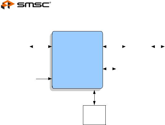
The LAN8720/LAN8720i is a low-power 10BASE-T/100BASE-TX physical layer (PHY) transceiver that transmits and receives on unshielded twisted-pair cable. A typical system application is shown in Figure 1.2. It is available in both extended commercial and industrial temperature operating versions.
The LAN8720/LAN8720i interfaces to the MAC layer using a variable voltage digital interface via the RMII interface. The digital interface pins are tolerant to 3.6V.
The LAN8720/LAN8720i implements Auto-Negotiation to automatically determine the best possible speed and duplex mode of operation. HP Auto-MDIX support allows using a direct connect LAN cable, or a cross-over path cable.
The LAN8720 referenced throughout this document applies to both the extended commercial temperature and industrial temperature components. The LAN8720i refers to only the industrial temperature component.
SMSC LAN8720/LAN8720i |
9 |
Revision 1.0 (05-28-09) |
|
DATASHEET |
|
Small Footprint RMII 10/100 Ethernet Transceiver with HP Auto-MDIX Support
Datasheet
10/100 |
|
|
|
MDI |
|
|
|
|
|
|
|
|
|
|
|
|
|
|
|
|
|||
Ethernet |
|
|
|
|
Transformer |
|
|
|
RJ45 |
||
|
|
|
|
|
|
|
|
|
|||
MAC |
|
LAN8720 |
|
|
|
|
|
|
|||
|
|
|
|
|
|
|
|
|
|||
|
RMII |
Ethernet |
|
|
|
|
|
|
|||
|
|
|
|
|
|
|
|||||
|
|
|
Transceiver |
|
|
|
|
|
|
|
|
MODE |
LED Status |
|
Crystal or
Clock Osc
Figure 1.1 LAN8720/LAN8720i System Block Diagram
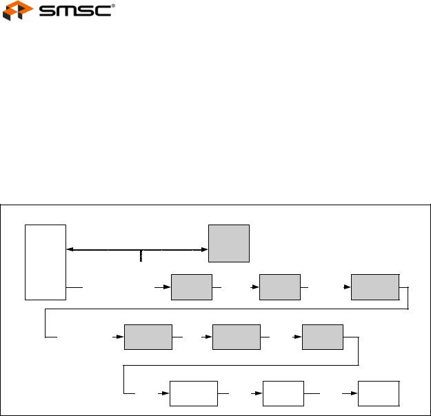
1.3Architectural Overview
The LAN8720/LAN8720i is compliant with IEEE 802.3-2005 standards (RMII Pins tolerant to 3.6V) and supports both IEEE 802.3-2005 compliant and vendor-specific register functions. It contains a fullduplex 10-BASE-T/100BASE-TX transceiver and supports 10-Mbps (10BASE-T) operation, and 100Mbps (100BASE-TX) operation. The LAN8720/LAN8720i can be configured to operate on a single 3.3V supply utilizing an integrated 3.3V to 1.2V linear regulator. An option is available to disable the linear regulator to optimize system designs that have a 1.2V power supply available. This allows for the use of a high efficiency external regulator for lower system power dissipation.
1.3.1Configuration
The LAN8720 will begin normal operation following reset, and no register access is required. The initial configuration may be selected with configuration pins as described in Section 5.3.9. In addition, register-selectable configuration options may be used to further define the functionality of the transceiver. For example, the device can be set to 10BASE-T only. The LAN8720 supports both IEEE 802.3-2005 compliant and vendor-specific register functions.
Revision 1.0 (05-28-09) |
10 |
SMSC LAN8720/LAN8720i |
|
DATASHEET |
|

Small Footprint RMII 10/100 Ethernet Transceiver with HP Auto-MDIX Support
Datasheet |
|
|
|
|
|
|
MODE0 |
|
Auto- |
10M Tx |
10M |
HP Auto-MDIX |
|
MODE1 |
MODE Control |
|
|
|||
Negotiation |
Logic |
Transmitter |
|
TXP / TXN |
||
MODE2 |
|
|
||||
nRST |
Reset |
|
Transmit Section |
|
RXP / RXN |
|
Control |
Management |
100M Tx |
100M |
|
||
|
SMI |
|
|
|||
|
Control |
Logic |
Transmitter |
|
|
|
|
|
MDIX |
|
|||
|
|
|
|
|
|
|
|
|
|
|
|
Control |
|
TXD[1:0] |
|
|
|
|
PLL |
XTAL1/CLKIN |
TXEN |
|
100M Rx |
DSP System: |
Analog-to- |
XTAL2 |
|
|
|
|
||||
|
|
Logic |
Clock |
Digital |
|
|
|
|
|
|
|||
|
|
|
Data Recovery |
|
Interrupt |
nINT |
|
|
|
Equalizer |
|
||
RXD[1:0] |
|
|
|
Generator |
||
RMII |
|
|
|
|
||
RXER |
Receive Section |
100M PLL |
|
|
||
|
|
|
||||
|
Logic |
|
|
|
LED Circuitry |
LED1 |
|
|
|
|
LED2 |
||
|
10M Rx |
|
Squelch & |
|
||
|
|
|
|
|
||
CRS_DV |
|
Logic |
|
Filters |
|
|
|
|
|
|
Central |
RBIAS |
|
|
|
|
|
|
||
MDC |
|
|
10M PLL |
|
Bias |
|
|
|
|
|
|||
MDIO |
|
|
|
|
PHY |
|
|
|
|
|
|
|
|
|
|
|
|
|
Address |
PHYAD0 |
|
|
|
|
|
Latches |
|
Figure 1.2 LAN8720/LAN8720i Architectural Overview
SMSC LAN8720/LAN8720i |
11 |
Revision 1.0 (05-28-09) |
|
DATASHEET |
|
Small Footprint RMII 10/100 Ethernet Transceiver with HP Auto-MDIX Support
Datasheet
Chapter 2 Pin Configuration
2.1Package Pin-out Diagram and Signal Table
|
RBIAS |
RXP |
RXN |
TXP |
TXN |
VDD1A |
|
|
|
24 |
23 |
22 |
21 |
20 |
19 |
|
|
VDD2A |
1 |
|
|
|
|
|
18 |
TXD1 |
LED2/nINTSEL |
2 |
|
SMSC |
|
|
17 |
TXD0 |
|
LED1/REGOFF |
3 |
|
LAN8720/ |
|
|
16 |
TXEN |
|
|
LAN8720i |
|
|
|||||
|
|
|
|
|
|
|
||
XTAL2 |
4 |
24 PIN QFN |
|
15 |
nRST |
|||
XTAL1/CLKIN |
5 |
|
(Top View) |
|
14 |
nINT/REFCLKO |
||
|
VSS |
|
|
|||||
VDDCR |
6 |
|
|
|
13 |
MDC |
||
|
|
10 |
11 |
12 |
||||
|
7 |
8 |
9 |
|
|
|||
|
RXD1/MODE1 |
RXD0/MDE0 |
VDDIO |
RXER/PHYAD0 |
CRS DV/MODE2 |
MDIO |
|
|
Figure 2.1 LAN8720/LAN8720i 24-QFN Pin Assignments (TOP VIEW)
Revision 1.0 (05-28-09) |
12 |
SMSC LAN8720/LAN8720i |
|
DATASHEET |
|

Small Footprint RMII 10/100 Ethernet Transceiver with HP Auto-MDIX Support
Datasheet
Table 2.1 LAN8720/LAN8720i 24-PIN QFN Pinout
PIN NO. |
PIN NAME |
PIN NO. |
PIN NAME |
|
|
|
|
1 |
VDD2A |
13 |
MDC |
|
|
|
|
2 |
LED2/nINTSEL |
14 |
nINT/REFCLKO |
|
|
|
|
3 |
LED1/REGOFF |
15 |
nRST |
|
|
|
|
4 |
XTAL2 |
16 |
TXEN |
|
|
|
|
5 |
XTAL1/CLKIN |
17 |
TXD0 |
|
|
|
|
6 |
VDDCR |
18 |
TXD1 |
|
|
|
|
7 |
RXD1/MODE1 |
19 |
VDD1A |
|
|
|
|
8 |
RXD0/MODE0 |
20 |
TXN |
|
|
|
|
9 |
VDDIO |
21 |
TXP |
|
|
|
|
10 |
RXER/PHYAD0 |
22 |
RXN |
|
|
|
|
11 |
CRS_DV/MODE2 |
23 |
RXP |
|
|
|
|
12 |
MDIO |
24 |
RBIAS |
|
|
|
|
SMSC LAN8720/LAN8720i |
13 |
Revision 1.0 (05-28-09) |
|
DATASHEET |
|

Small Footprint RMII 10/100 Ethernet Transceiver with HP Auto-MDIX Support
Datasheet
Chapter 3 Pin Description
This chapter describes the signals on each pin. When a lower case “n” is used at the beginning of the signal name, it indicates that the signal is active low. For example, nRST indicates that the reset signal is active low. The buffer type for each signal is indicated in the TYPE column, and a description of the buffer types is provided in Table 3.1.
|
Table 3.1 Buffer Types |
|
|
BUFFER TYPE |
DESCRIPTION |
|
|
I8 |
Input. |
|
|
O8 |
Output with 8mA sink and 8mA source. |
|
|
IOD8 |
Input/Open-drain output with 8mA sink. |
|
|
IPU |
Input with 67k (typical) internal pull-up. |
Note 3.1 |
|
|
|
IPD |
Input with 67k (typical) internal pull-down. |
Note 3.1 |
|
|
|
IOPU |
Input/Output with 67k (typical) internal pull-up. Output has 8mA sink and 8mA source. |
Note 3.1 |
|
|
|
IOPD |
Input/Output with 67k (typical) internal pull-down. Output has 8mA sink and 8mA source. |
Note 3.1 |
|
|
|
AI |
Analog input |
|
|
AIO |
Analog bi-directional |
|
|
ICLK |
Crystal oscillator input pin |
|
|
OCLK |
Crystal oscillator output pin |
|
|
P |
Power pin |
|
|
Note 3.1 Unless otherwise noted in the pin description, internal pull-up and pull-down resistors are always enabled. The internal pull-up and pull-down resistors prevent unconnected inputs from floating, and must not be relied upon to drive signals external to LAN8720/LAN8720i. When connected to a load that must be pulled high or low, an external resistor must be added.
Note: The digital signals are not 5V tolerant.They are variable voltage from +1.6V to +3.6V, as shown in Table 7.1.
Revision 1.0 (05-28-09) |
14 |
SMSC LAN8720/LAN8720i |
|
DATASHEET |
|

Small Footprint RMII 10/100 Ethernet Transceiver with HP Auto-MDIX Support
Datasheet
3.1MAC Interface Signals
|
|
|
Table 3.2 RMII Signals 24-QFN |
|
|
|
|
SIGNAL |
24-QFN |
|
|
NAME |
PIN # |
TYPE |
DESCRIPTION |
|
|
|
|
TXD0 |
17 |
I8 |
Transmit Data 0: The MAC transmits data to the PHY using this signal in |
|
|
|
all modes. |
|
|
|
|
TXD1 |
18 |
I8 |
Transmit Data 1: The MAC transmits data to the PHY using this signal in |
|
|
|
all modes |
|
|
|
|
TXEN |
16 |
IPD |
Transmit Enable: Indicates that valid data is presented on the TXD[1:0] |
|
|
|
signals, for transmission. |
|
|
|
|
RXD0/ |
8 |
IOPU |
Receive Data 0: Bit 0 of the 4 data bits that are sent by the PHY in the |
MODE0 |
|
|
receive path. |
|
|
|
PHY Operating Mode Bit 0: set the default MODE of the PHY. |
|
|
|
See Section 5.3.9.2 for information on the MODE options. |
|
|
|
|
RXD1/ |
7 |
IOPU |
Receive Data 1: Bit 1 of the 4 data bits that are sent by the PHY in the |
MODE1 |
|
|
receive path. |
|
|
|
PHY Operating Mode Bit 1: set the default MODE of the PHY. |
|
|
|
See Section 5.3.9.2 for information on the MODE options. |
|
|
|
|
RXER/ |
10 |
IOPD |
Receive Error: Asserted to indicate that an error was detected somewhere |
PHYAD0 |
|
|
in the frame presently being transferred from the PHY. |
|
|
|
The RXER signal is optional in RMII Mode. |
|
|
|
This signal is mux’d with PHYAD0 |
|
|
|
See Section 5.3.9.1 for information on the ADDRESS options. |
|
|
|
|
CRS_DV/ |
11 |
IOPU |
RMII Mode CRS_DV (Carrier Sense/Receive Data Valid) Asserted to |
MODE2 |
|
|
indicate when the receive medium is non-idle. When a 10BT packet is |
|
|
|
received, CRS_DV is asserted, but RXD[1:0] is held low until the SFD byte |
|
|
|
(10101011) is received. In 10BT, half-duplex mode, transmitted data is not |
|
|
|
looped back onto the receive data pins, per the RMII standard. |
|
|
|
PHY Operating Mode Bit 2: set the default MODE of the PHY. |
|
|
|
See Section 5.3.9.2 for information on the MODE options. |
|
|
|
|
3.2LED Signals
|
|
|
Table 3.3 LED Signals 24-QFN |
|
|
|
|
SIGNAL |
24-QFN |
|
|
NAME |
PIN # |
TYPE |
DESCRIPTION |
|
|
|
|
LED1/ |
3 |
IOPD |
LED1 – Link activity LED Indication. |
REGOFF |
|
|
See Section 5.3.7 for a description of LED modes. |
|
|
|
Regulator Off: This pin may be used to configure the internal 1.2V regulator |
|
|
|
off. As described in Section 4.11, this pin is sampled during the power-on |
|
|
|
sequence to determine if the internal regulator should turn on. When the |
|
|
|
regulator is disabled, external 1.2V must be supplied to VDDCR. |
|
|
|
When LED1/REGOFF is pulled high to VDD2A with an external resistor, the |
|
|
|
internal regulator is disabled. |
|
|
|
When LED1/REGOFF is floating or pulled low, the internal regulator is |
|
|
|
enabled (default). |
|
|
|
|
SMSC LAN8720/LAN8720i |
15 |
Revision 1.0 (05-28-09) |
|
DATASHEET |
|

|
|
|
|
Small Footprint RMII 10/100 Ethernet Transceiver with HP Auto-MDIX Support |
|
|
|
|
Datasheet |
|
|
|
Table 3.3 LED Signals 24-QFN (continued) |
|
|
|
|
|
|
SIGNAL |
24-QFN |
|
|
|
NAME |
PIN # |
TYPE |
|
DESCRIPTION |
|
|
|
|
|
LED2/ |
2 |
IOPU |
|
LED2 – Link speed LED Indication. |
nINTSEL |
|
|
|
See Section 5.3.7 for a description of LED modes. |
|
|
|
|
nINTSEL: On power-up or external reset, the mode of the nINT/REFCLKO |
|
|
|
|
pin is selected. |
|
|
|
|
See Section 4.10 for additional detail. |
|
|
|
|
When LED2/nINTSEL is floated or pulled to VDD2A, nINT is selected for |
|
|
|
|
operation on pin nINT/REFCLKO (default). |
|
|
|
|
When LED2/nINTSEL is pulled low to VSS through a resistor, REFCLKO is |
|
|
|
|
selected for operation on pin nINT/REFCLKO. |
|
|
|
|
|
3.3Management Signals
|
|
|
Table 3.4 Management Signals 24-QFN |
|
|
|
|
SIGNAL |
24-QFN |
|
|
NAME |
PIN # |
TYPE |
DESCRIPTION |
|
|
|
|
MDIO |
12 |
IOD8 |
Management Data Input/OUTPUT: Serial management data input/output. |
|
|
|
|
MDC |
13 |
I8 |
Management Clock: Serial management clock. |
|
|
|
|
3.4General Signals
|
|
|
Table 3.5 General Signals 24-QFN |
|
|
|
|
SIGNAL |
24-QFN |
|
|
NAME |
PIN # |
TYPE |
DESCRIPTION |
|
|
|
|
nINT/ |
14 |
IOPU |
nINT – Active low interrupt output. Place an external resistor pull-up to |
REFCLKO |
|
|
VDDIO. |
|
|
|
REFCLKO – 50MHz clock derived from the 25MHz crystal oscillator. |
|
|
|
See Section 4.7.2 for additional detail. |
|
|
|
See DESCRIPTION of pin 2: LED2 – Link speed LED Indication. |
|
|
|
This signal is mux’d with REFCLKO. |
|
|
|
|
XTAL1/ |
5 |
ICLK |
Clock Input: Crystal connection or external clock input. |
CLKIN |
|
|
|
|
|
|
|
XTAL2 |
4 |
OCL |
Clock Output: Crystal connection. |
|
|
K |
Float this pin when an external clock is driven to XTAL1/CLKIN. |
|
|
|
|
nRST |
15 |
IOPU |
External Reset: Input of the system reset. This signal is active LOW. |
|
|
|
|
Revision 1.0 (05-28-09) |
16 |
SMSC LAN8720/LAN8720i |
|
DATASHEET |
|

Small Footprint RMII 10/100 Ethernet Transceiver with HP Auto-MDIX Support
Datasheet
3.510/100 Line Interface Signals
|
|
Table 3.6 |
10/100 Line Interface Signals 24-QFN |
|
|
|
|
|
|
SIGNAL |
24-QFN |
|
|
|
NAME |
PIN # |
TYPE |
|
DESCRIPTION |
|
|
|
|
|
TXP |
21 |
AIO |
Transmit/Receive Positive Channel 1. |
|
|
|
|
|
|
TXN |
20 |
AIO |
Transmit/Receive Negative Channel 1. |
|
|
|
|
|
|
RXP |
23 |
AIO |
Transmit/Receive Positive Channel 2. |
|
|
|
|
|
|
RXN |
22 |
AIO |
Transmit/Receive Negative Channel 2. |
|
|
|
|
|
|
3.6Analog Reference
|
|
|
Table 3.7 Analog References 24-QFN |
|
|
|
|
SIGNAL |
24-QFN |
|
|
NAME |
PIN # |
TYPE |
DESCRIPTION |
|
|
|
|
RBIAS |
24 |
AI |
External 1% Bias Resistor. Requires an 12.1k resistor to ground connected |
|
|
|
as described in the Analog Layout Guidelines. The nominal voltage is 1.2V |
|
|
|
and therefore the resistor will dissipate approximately 1mW of power. |
|
|
|
|
3.7Power Signals
Table 3.8 Power Signals 24-QFN
SIGNAL |
24-QFN |
|
|
|
NAME |
PIN # |
TYPE |
|
DESCRIPTION |
|
|
|
|
|
VDDIO |
9 |
P |
+1.6V to +3.6V Variable I/O Pad Power |
|
|
|
|
|
|
VDDCR |
6 |
P |
+1.2V |
(Core voltage) - 1.2V for digital circuitry on chip. Supplied by the on- |
|
|
|
chip regulator unless configured for regulator off mode using the |
|
|
|
|
RXCLK/REGOFF pin. A 1uF decoupling capacitor to ground should be used |
|
|
|
|
on this pin when using the internal 1.2V regulator. |
|
|
|
|
|
|
VDD1A |
19 |
P |
+3.3V |
Analog Port Power to Channel 1. |
|
|
|
|
|
VDD2A |
1 |
P |
+3.3V |
Analog Port Power to Channel 2 and to internal regulator. |
|
|
|
|
|
VSS |
FLAG |
GND |
The flag must be connected to the ground plane with a via array under the |
|
|
|
|
exposed flag. This is the ground connection for the IC. |
|
|
|
|
|
|
SMSC LAN8720/LAN8720i |
17 |
Revision 1.0 (05-28-09) |
|
DATASHEET |
|
Small Footprint RMII 10/100 Ethernet Transceiver with HP Auto-MDIX Support
Datasheet
Chapter 4 Architecture Details
4.1Top Level Functional Architecture
Functionally, the transceiver can be divided into the following sections:
100Base-TX transmit and receive
10Base-T transmit and receive
RMII interface to the controller
Auto-negotiation to automatically determine the best speed and duplex possible
Management Control to read status registers and write control registers
|
|
|
|
PLL |
|
|
|
MAC |
|
Ref_CLK |
|
|
|
|
|
|
|
|
|
|
|
|
|
|
RMII 50Mhz by 2 bits |
RMII |
25MHz |
4B/5B |
25MHz by |
Scrambler |
|
|
by 4 bits |
Encoder |
5 bits |
and PISO |
|||
|
|
|
|
||||
|
125 Mbps Serial |
NRZI |
NRZI |
MLT-3 |
MLT-3 |
Tx |
|
|
Converter |
Converter |
Driver |
|
|||
|
|
|
|
|
|||
|
|
MLT-3 |
Magnetics |
MLT-3 |
RJ45 |
MLT-3 |
CAT-5 |
Figure 4.1 100Base-TX Data Path
4.2100Base-TX Transmit
The data path of the 100Base-TX is shown in Figure 4.1. Each major block is explained below.
4.2.1100M Transmit Data Across the MII/RMII Interface
For MII, the MAC controller drives the transmit data onto the TXD bus and asserts TXEN to indicate valid data. The data is latched by the transceiver’s MII block on the rising edge of TXCLK. The data is in the form of 4-bit wide 25MHz data.
For RMII, the MAC controller drives the transmit data onto the TXD bus and asserts TXEN to indicate valid data. The data is latched by the transceiver’s RMII block on the rising edge of REF_CLK. The data is in the form of 2-bit wide 50MHz data.
Revision 1.0 (05-28-09) |
18 |
SMSC LAN8720/LAN8720i |
|
DATASHEET |
|

Small Footprint RMII 10/100 Ethernet Transceiver with HP Auto-MDIX Support
Datasheet
4.2.24B/5B Encoding
The transmit data passes from the MII block to the 4B/5B encoder. This block encodes the data from 4-bit nibbles to 5-bit symbols (known as “code-groups”) according to Table 4.1. Each 4-bit data-nibble is mapped to 16 of the 32 possible code-groups. The remaining 16 code-groups are either used for control information or are not valid.
The first 16 code-groups are referred to by the hexadecimal values of their corresponding data nibbles, 0 through F. The remaining code-groups are given letter designations with slashes on either side. For example, an IDLE code-group is /I/, a transmit error code-group is /H/, etc.
The encoding process may be bypassed by clearing bit 6 of register 31. When the encoding is bypassed the 5th transmit data bit is equivalent to TXER.
Note that encoding can be bypassed only when the MAC interface is configured to operate in MII mode.
Table 4.1 4B/5B Code Table
CODE |
|
|
|
RECEIVER |
|
|
TRANSMITTER |
|
|||
GROUP |
SYM |
|
INTERPRETATION |
|
|
INTERPRETATION |
|
||||
|
|
|
|
|
|
|
|
|
|
|
|
11110 |
0 |
0 |
|
0000 |
|
DATA |
0 |
|
0000 |
|
DATA |
|
|
|
|
|
|
|
|
|
|
|
|
01001 |
1 |
1 |
|
0001 |
|
|
1 |
|
0001 |
|
|
|
|
|
|
|
|
|
|
|
|
|
|
10100 |
2 |
2 |
|
0010 |
|
|
2 |
|
0010 |
|
|
|
|
|
|
|
|
|
|
|
|
|
|
10101 |
3 |
3 |
|
0011 |
|
|
3 |
|
0011 |
|
|
|
|
|
|
|
|
|
|
|
|
|
|
01010 |
4 |
4 |
|
0100 |
|
|
4 |
|
0100 |
|
|
|
|
|
|
|
|
|
|
|
|
|
|
01011 |
5 |
5 |
|
0101 |
|
|
5 |
|
0101 |
|
|
|
|
|
|
|
|
|
|
|
|
|
|
01110 |
6 |
6 |
|
0110 |
|
|
6 |
|
0110 |
|
|
|
|
|
|
|
|
|
|
|
|
|
|
01111 |
7 |
7 |
|
0111 |
|
|
7 |
|
0111 |
|
|
|
|
|
|
|
|
|
|
|
|
|
|
10010 |
8 |
8 |
|
1000 |
|
|
8 |
|
1000 |
|
|
|
|
|
|
|
|
|
|
|
|
|
|
10011 |
9 |
9 |
|
1001 |
|
|
9 |
|
1001 |
|
|
|
|
|
|
|
|
|
|
|
|
|
|
10110 |
A |
A |
|
1010 |
|
|
A |
|
1010 |
|
|
|
|
|
|
|
|
|
|
|
|
|
|
10111 |
B |
B |
|
1011 |
|
|
B |
|
1011 |
|
|
|
|
|
|
|
|
|
|
|
|
|
|
11010 |
C |
C |
|
1100 |
|
|
C |
|
1100 |
|
|
|
|
|
|
|
|
|
|
|
|
|
|
11011 |
D |
D |
|
1101 |
|
|
D |
|
1101 |
|
|
|
|
|
|
|
|
|
|
|
|
|
|
11100 |
E |
E |
|
1110 |
|
|
E |
|
1110 |
|
|
|
|
|
|
|
|
|
|
|
|
|
|
11101 |
F |
F |
|
1111 |
|
|
F |
|
1111 |
|
|
|
|
|
|
|
|
|
|
|
|
|
|
11111 |
I |
IDLE |
|
|
|
|
Sent after /T/R until TXEN |
|
|||
|
|
|
|
|
|||||||
11000 |
J |
First nibble of SSD, translated to “0101” |
Sent for rising TXEN |
|
|||||||
|
|
following IDLE, else RXER |
|
|
|
|
|
|
|||
|
|
|
|
|
|||||||
10001 |
K |
Second nibble of SSD, translated to |
Sent for rising TXEN |
|
|||||||
|
|
“0101” following J, else RXER |
|
|
|
|
|
|
|||
|
|
|
|
|
|||||||
01101 |
T |
First nibble of ESD, causes de-assertion |
Sent for falling TXEN |
|
|||||||
|
|
of CRS if followed by /R/, else assertion |
|
|
|
|
|
||||
|
|
of RXER |
|
|
|
|
|
|
|
|
|
|
|
|
|
|
|
|
|
|
|
|
|
SMSC LAN8720/LAN8720i |
19 |
Revision 1.0 (05-28-09) |
|
DATASHEET |
|

|
|
|
Small Footprint RMII 10/100 Ethernet Transceiver with HP Auto-MDIX Support |
|
|
|
|
|
Datasheet |
|
|
Table 4.1 4B/5B Code Table (continued) |
||
|
|
|
|
|
CODE |
|
RECEIVER |
|
TRANSMITTER |
GROUP |
SYM |
INTERPRETATION |
|
INTERPRETATION |
|
|
|
|
|
00111 |
R |
Second nibble of ESD, causes |
|
Sent for falling TXEN |
|
|
deassertion of CRS if following /T/, else |
|
|
|
|
assertion of RXER |
|
|
|
|
|
|
|
00100 |
H |
Transmit Error Symbol |
|
Sent for rising TXER |
|
|
|
|
|
00110 |
V |
INVALID, RXER if during RXDV |
|
INVALID |
|
|
|
|
|
11001 |
V |
INVALID, RXER if during RXDV |
|
INVALID |
|
|
|
|
|
00000 |
V |
INVALID, RXER if during RXDV |
|
INVALID |
|
|
|
|
|
00001 |
V |
INVALID, RXER if during RXDV |
|
INVALID |
|
|
|
|
|
00010 |
V |
INVALID, RXER if during RXDV |
|
INVALID |
|
|
|
|
|
00011 |
V |
INVALID, RXER if during RXDV |
|
INVALID |
|
|
|
|
|
00101 |
V |
INVALID, RXER if during RXDV |
|
INVALID |
|
|
|
|
|
01000 |
V |
INVALID, RXER if during RXDV |
|
INVALID |
|
|
|
|
|
01100 |
V |
INVALID, RXER if during RXDV |
|
INVALID |
|
|
|
|
|
10000 |
V |
INVALID, RXER if during RXDV |
|
INVALID |
|
|
|
|
|
4.2.3Scrambling
Repeated data patterns (especially the IDLE code-group) can have power spectral densities with large narrow-band peaks. Scrambling the data helps eliminate these peaks and spread the signal power more uniformly over the entire channel bandwidth. This uniform spectral density is required by FCC regulations to prevent excessive EMI from being radiated by the physical wiring.
The seed for the scrambler is generated from the transceiver address, PHYAD[4:0], ensuring that in multiple-transceiver applications, such as repeaters or switches, each transceiver will have its own scrambler sequence.
The scrambler also performs the Parallel In Serial Out conversion (PISO) of the data.
4.2.4NRZI and MLT3 Encoding
The scrambler block passes the 5-bit wide parallel data to the NRZI converter where it becomes a serial 125MHz NRZI data stream. The NRZI is encoded to MLT-3. MLT3 is a tri-level code where a change in the logic level represents a code bit “1” and the logic output remaining at the same level represents a code bit “0”.
4.2.5100M Transmit Driver
The MLT3 data is then passed to the analog transmitter, which drives the differential MLT-3 signal, on outputs TXP and TXN, to the twisted pair media across a 1:1 ratio isolation transformer. The 10Base- T and 100Base-TX signals pass through the same transformer so that common “magnetics” can be used for both. The transmitter drives into the 100Ω impedance of the CAT-5 cable. Cable termination and impedance matching require external components.
Revision 1.0 (05-28-09) |
20 |
SMSC LAN8720/LAN8720i |
|
DATASHEET |
|
Small Footprint RMII 10/100 Ethernet Transceiver with HP Auto-MDIX Support
Datasheet
4.2.6100M Phase Lock Loop (PLL)
The 100M PLL locks onto reference clock and generates the 125MHz clock used to drive the 125 MHz logic and the 100Base-Tx Transmitter.
|
|
|
|
PLL |
|
|
|
MAC |
|
Ref_CLK |
|
|
|
|
|
|
|
|
|
|
|
|
|
|
RMII 50Mhz by 2 bits |
RMII |
25MHz |
4B/5B |
25MHz by |
Scrambler |
|
|
by 4 bits |
Encoder |
5 bits |
and PISO |
|||
|
|
|
|
||||
|
125 Mbps Serial |
NRZI |
NRZI |
MLT-3 |
MLT-3 |
Tx |
|
|
Converter |
Converter |
Driver |
|
|||
|
|
|
|
|
|||
|
|
MLT-3 |
Magnetics |
MLT-3 |
RJ45 |
MLT-3 |
CAT-5 |
Figure 4.2 Receive Data Path
4.3100Base-TX Receive
The receive data path is shown in Figure 4.2. Detailed descriptions are given below.
4.3.1100M Receive Input
The MLT-3 from the cable is fed into the transceiver (on inputs RXP and RXN) via a 1:1 ratio transformer. The ADC samples the incoming differential signal at a rate of 125M samples per second. Using a 64-level quanitizer it generates 6 digital bits to represent each sample. The DSP adjusts the gain of the ADC according to the observed signal levels such that the full dynamic range of the ADC can be used.
4.3.2Equalizer, Baseline Wander Correction and Clock and Data Recovery
The 6 bits from the ADC are fed into the DSP block. The equalizer in the DSP section compensates for phase and amplitude distortion caused by the physical channel consisting of magnetics, connectors, and CAT- 5 cable. The equalizer can restore the signal for any good-quality CAT-5 cable between 1m and 150m.
If the DC content of the signal is such that the low-frequency components fall below the low frequency pole of the isolation transformer, then the droop characteristics of the transformer will become significant and Baseline Wander (BLW) on the received signal will result. To prevent corruption of the received data, the transceiver corrects for BLW and can receive the ANSI X3.263-1995 FDDI TP-PMD defined “killer packet” with no bit errors.
The 100M PLL generates multiple phases of the 125MHz clock. A multiplexer, controlled by the timing unit of the DSP, selects the optimum phase for sampling the data. This is used as the received recovered clock. This clock is used to extract the serial data from the received signal.
SMSC LAN8720/LAN8720i |
21 |
Revision 1.0 (05-28-09) |
|
DATASHEET |
|

Small Footprint RMII 10/100 Ethernet Transceiver with HP Auto-MDIX Support
Datasheet
4.3.3NRZI and MLT-3 Decoding
The DSP generates the MLT-3 recovered levels that are fed to the MLT-3 converter. The MLT-3 is then converted to an NRZI data stream.
4.3.4Descrambling
The descrambler performs an inverse function to the scrambler in the transmitter and also performs the Serial In Parallel Out (SIPO) conversion of the data.
During reception of IDLE (/I/) symbols. the descrambler synchronizes its descrambler key to the incoming stream. Once synchronization is achieved, the descrambler locks on this key and is able to descramble incoming data.
Special logic in the descrambler ensures synchronization with the remote transceiver by searching for IDLE symbols within a window of 4000 bytes (40us). This window ensures that a maximum packet size of 1514 bytes, allowed by the IEEE 802.3 standard, can be received with no interference. If no IDLEsymbols are detected within this time-period, receive operation is aborted and the descrambler re-starts the synchronization process.
The descrambler can be bypassed by setting bit 0 of register 31.
4.3.5Alignment
The de-scrambled signal is then aligned into 5-bit code-groups by recognizing the /J/K/ Start-of-Stream Delimiter (SSD) pair at the start of a packet. Once the code-word alignment is determined, it is stored and utilized until the next start of frame.
4.3.65B/4B Decoding
The 5-bit code-groups are translated into 4-bit data nibbles according to the 4B/5B table. The translated data is presented on the RXD[3:0] signal lines. The SSD, /J/K/, is translated to “0101 0101” as the first 2 nibbles of the MAC preamble. Reception of the SSD causes the transceiver to assert the RXDV signal, indicating that valid data is available on the RXD bus. Successive valid code-groups are translated to data nibbles. Reception of either the End of Stream Delimiter (ESD) consisting of the /T/R/ symbols, or at least two /I/ symbols causes the transceiver to de-assert carrier sense and RXDV.
These symbols are not translated into data.
The decoding process may be bypassed by clearing bit 6 of register 31. When the decoding is bypassed the 5th receive data bit is driven out on RXER/RXD4/PHYAD0. Decoding may be bypassed only when the MAC interface is in MII mode.
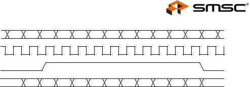
4.3.7Receive Data Valid Signal
The Receive Data Valid signal (RXDV) indicates that recovered and decoded nibbles are being presented on the RXD[3:0] outputs synchronous to RXCLK. RXDV becomes active after the /J/K/ delimiter has been recognized and RXD is aligned to nibble boundaries. It remains active until either the /T/R/ delimiter is recognized or link test indicates failure or SIGDET becomes false.
RXDV is asserted when the first nibble of translated /J/K/ is ready for transfer over the Media Independent Interface (MII mode).
Revision 1.0 (05-28-09) |
22 |
SMSC LAN8720/LAN8720i |
|
DATASHEET |
|
Small Footprint RMII 10/100 Ethernet Transceiver with HP Auto-MDIX Support
Datasheet
CLEAR-TEXT |
J K 5 |
5 |
5 |
D |
data |
data |
data |
data |
T |
R Idle |
RX_CLK |
|
|
|
|
|
|
|
|
|
|
RX_DV |
|
|
|
|
|
|
|
|
|
|
RXD |
5 |
5 |
5 |
5 |
5 |
D |
data |
data |
data |
data |
Figure 4.3 Relationship Between Received Data and Specific MII Signals
4.3.8Receiver Errors
During a frame, unexpected code-groups are considered receive errors. Expected code groups are the DATA set (0 through F), and the /T/R/ (ESD) symbol pair. When a receive error occurs, the RXER signal is asserted and arbitrary data is driven onto the RXD[3:0] lines. Should an error be detected during the time that the /J/K/ delimiter is being decoded (bad SSD error), RXER is asserted true and the value ‘1110’ is driven onto the RXD[3:0] lines. Note that the Valid Data signal is not yet asserted when the bad SSD error occurs.
4.3.9100M Receive Data Across the MII/RMII Interface
In MII mode, the 4-bit data nibbles are sent to the MII block. These data nibbles are clocked to the controller at a rate of 25MHz. The controller samples the data on the rising edge of RXCLK. To ensure that the setup and hold requirements are met, the nibbles are clocked out of the transceiver on the falling edge of RXCLK. RXCLK is the 25MHz output clock for the MII bus. It is recovered from the received data to clock the RXD bus. If there is no received signal, it is derived from the system reference clock (XTAL1/CLKIN).
When tracking the received data, RXCLK has a maximum jitter of 0.8ns (provided that the jitter of the input clock, XTAL1/CLKIN, is below 100ps).
In RMII mode, the 2-bit data nibbles are sent to the RMII block. These data nibbles are clocked to the controller at a rate of 50MHz. The controller samples the data on the rising edge of XTAL1/CLKIN (REF_CLK). To ensure that the setup and hold requirements are met, the nibbles are clocked out of the transceiver on the falling edge of XTAL1/CLKIN (REF_CLK).
4.410Base-T Transmit
Data to be transmitted comes from the MAC layer controller. The 10Base-T transmitter receives 4-bit nibbles from the MII at a rate of 2.5MHz and converts them to a 10Mbps serial data stream. The data stream is then Manchester-encoded and sent to the analog transmitter, which drives a signal onto the twisted pair via the external magnetics.
The 10M transmitter uses the following blocks:
MII (digital)
TX 10M (digital)
10M Transmitter (analog)
10M PLL (analog)
4.4.110M Transmit Data Across the MII/RMII Interface
The MAC controller drives the transmit data onto the TXD BUS. For MII, when the controller has driven TXEN high to indicate valid data, the data is latched by the MII block on the rising edge of TXCLK. The data is in the form of 4-bit wide 2.5MHz data.
SMSC LAN8720/LAN8720i |
23 |
Revision 1.0 (05-28-09) |
|
DATASHEET |
|

Small Footprint RMII 10/100 Ethernet Transceiver with HP Auto-MDIX Support
Datasheet
In order to comply with legacy 10Base-T MAC/Controllers, in Half-duplex mode the transceiver loops back the transmitted data, on the receive path. This does not confuse the MAC/Controller since the COL signal is not asserted during this time. The transceiver also supports the SQE (Heartbeat) signal. See Section 5.3.2, "Collision Detect," on page 50, for more details.
For RMII, TXD[1:0] shall transition synchronously with respect to REF_CLK. When TXEN is asserted, TXD[1:0] are accepted for transmission by the LAN8720/LAN8720i. TXD[1:0] shall be “00” to indicate idle when TXEN is deasserted. Values of TXD[1:0] other than “00” when TXEN is deasserted are reserved for out-of-band signalling (to be defined). Values other than “00” on TXD[1:0] while TXEN is deasserted shall be ignored by the LAN8720/LAN8720i.TXD[1:0] shall provide valid data for each REF_CLK period while TXEN is asserted.
4.4.2Manchester Encoding
The 4-bit wide data is sent to the TX10M block. The nibbles are converted to a 10Mbps serial NRZI data stream. The 10M PLL locks onto the external clock or internal oscillator and produces a 20MHz clock. This is used to Manchester encode the NRZ data stream. When no data is being transmitted (TXEN is low), the TX10M block outputs Normal Link Pulses (NLPs) to maintain communications with the remote link partner.
4.4.310M Transmit Drivers
The Manchester encoded data is sent to the analog transmitter where it is shaped and filtered before being driven out as a differential signal across the TXP and TXN outputs.
4.510Base-T Receive
The 10Base-T receiver gets the Manchesterencoded analog signal from the cable via the magnetics. It recovers the receive clock from the signal and uses this clock to recover the NRZI data stream. This 10M serial data is converted to 4-bit data nibbles which are passed to the controller across the MII at a rate of 2.5MHz.
This 10M receiver uses the following blocks:
Filter and SQUELCH (analog)
10M PLL (analog)
RX 10M (digital)
MII (digital)
4.5.110M Receive Input and Squelch
The Manchester signal from the cable is fed into the transceiver (on inputs RXP and RXN) via 1:1 ratio magnetics. It is first filtered to reduce any out-of-band noise. It then passes through a SQUELCH circuit. The SQUELCH is a set of amplitude and timing comparators that normally reject differential voltage levels below 300mV and detect and recognize differential voltages above 585mV.
4.5.2Manchester Decoding
The output of the SQUELCH goes to the RX10M block where it is validated as Manchester encoded data. The polarity of the signal is also checked. If the polarity is reversed (local RXP is connected to RXN of the remote partner and vice versa), then this is identified and corrected. The reversed condition is indicated by the flag “XPOL“, bit 4 in register 27. The 10M PLL is locked onto the received Manchester signal and from this, generates the received 20MHz clock. Using this clock, the Manchester encoded data is extracted and converted to a 10MHz NRZI data stream. It is then converted from serial to 4-bit wide parallel data.
The RX10M block also detects valid 10Base-T IDLE signals - Normal Link Pulses (NLPs) - to maintain the link.
Revision 1.0 (05-28-09) |
24 |
SMSC LAN8720/LAN8720i |
|
DATASHEET |
|
 Loading...