


Silicon Storage Technology Inc SST37VF512-90-3C-WH, SST37VF010-70-3C-PH, SST37VF010-70-3C-NH, SST37VF512-90-3C-PH, SST37VF512-90-3C-NH Datasheet
...512 Kbit / 1 Mbit / 2 Mbit / 4 Mbit (x8) Many-Time Programmable Flash
SST37VF512 / SST37VF010 / SST37VF020 / SST37VF040
Data Sheet
FEATURES:
•Organized as 64K x8 / 128K x8 / 256K x8 / 512K x8
•2.7-3.6V Read Operation
•Superior Reliability
–Endurance: At least 1000 Cycles
–Greater than 100 years Data Retention
•Low Power Consumption:
–Active Current: 10 mA (typical)
–Standby Current: 2 µA (typical)
•Fast Read Access Time:
–70 ns
–90 ns
•Latched Address and Data
•Fast Byte-Program Operation:
–Byte-Program Time: 10 µs (typical)
–Chip Program Time:
0.6seconds (typical) for SST37VF512
1.2seconds (typical) for SST37VF010
2.4seconds (typical) for SST37VF020
4.8seconds (typical) for SST37VF040
•Electrical Erase Using Programmer
–Does not require UV source
–Chip-Erase Time: 100 ms (typical)
•CMOS I/O Compatibility
•JEDEC Standard Byte-wide Flash EEPROM Pinouts
•Packages Available
–32-pin PLCC
–32-pin TSOP (8mm x 14mm)
–32-pin PDIP
PRODUCT DESCRIPTION
The SST37VF512/010/020/040 devices are 64K x8 / 128K x8 / 256K x8 / 512K x8 CMOS, Many-Time Programmable (MTP), low cost flash, manufactured with SST’s proprietary, high performance CMOS SuperFlash technology. The split-gate cell design and thick oxide tunneling injector attain better reliability and manufacturability compared with alternate approaches. The SST37VF512/010/020/040 can be electrically erased and programmed at least 1000 times using an external programmer, e.g., to change the contents of devices in inventory. The SST37VF512/010/020/040 have to be erased prior to programming. These devices conform to JEDEC standard pinouts for byte-wide flash memories.
Featuring high performance Byte-Program, the SST37VF512/010/020/040 provide a typical Byte-Pro- gram time of 10 µs. Designed, manufactured, and tested for a wide spectrum of applications, these devices are offered with an endurance of at least 1000 cycles. Data retention is rated at greater than 100 years.
The SST37VF512/010/020/040 are suited for applications that require infrequent writes and low power nonvolatile storage. These devices will improve flexibility, efficiency, and performance while matching the low cost in nonvolatile applications that currently use UV-EPROMs, OTPs, and mask ROMs.
To meet surface mount and conventional through hole requirements, the SST37VF512/010/020/040 are offered in 32-pin PLCC, TSOP, and PDIP packages. See Figures 1, 2, and 3 for pinouts.
Device Operation
The SST37VF512/010/020/040 devices are nonvolatile memory solutions that can be used instead of standard flash devices if in-system programmability is not required. It is functionally (Read) and pin compatible with industry standard flash products.The device supports electrical Erase operation via an external programmer.
Read
The Read operation of the SST37VF512/010/020/040 is controlled by CE# and OE#. Both CE# and OE# have to be low for the system to obtain data from the outputs. Once the address is stable, the address access time is equal to the delay from CE# to output (TCE). Data is available at the output after a delay of TOE from the falling edge of OE#, assuming the CE# pin has been low and the addresses have been stable for at least TCE - TOE. When the CE# pin is high, the chip is deselected and a standby current of only 10 µA (typical) is consumed. OE# is the output control and is used to gate data from the output pins. The data bus is in high impedance state when either CE# or OE# is VIH. Refer to Figure 4 for the timing diagram.
©2001 Silicon Storage Technology, Inc. |
The SST logo and SuperFlash are registered trademarks of Silicon Storage Technology, Inc. |
|
S71151-02-000 5/01 |
397 |
MTP is a trademark of Silicon Storage Technology, Inc. |
|
|
These specifications are subject to change without notice. |
512 Kbit / 1 Mbit / 2 Mbit / 4 Mbit Multi-Purpose Flash SST37VF512 / SST37VF010 / SST37VF020 / SST37VF040
Byte-Program Operation
The SST37VF512/010/020/040 are programmed by using an external programmer. The programming mode is activated by asserting 12V (±5%) on OE# pin and VIL on CE# pin. The device is programmed using a single pulse (WE# pin low) of 10 µs per byte. Using the MTP programming algorithm, the Byte-Program process continues byte-by- byte until the entire chip has been programmed. Refer to Figure 10 for the flowchart and Figure 6 for the timing diagram.
Chip-Erase Operation
The only way to change a data from a “0” to “1” is by electrical erase that changes every bit in the device to “1”. The SST37VF512/010/020/040 use an electrical Chip-Erase operation. The entire chip can be erased in 100 ms (WE# pin low). In order to activate erase mode, the 12V (±5%) is applied to OE# and A9 pins while CE# is low. All other address and data pins are “don’t care”. The falling edge of WE# will start the Chip-Erase operation. Once the chip has been erased, all bytes must be verified for FFH. Refer to Figure 9 for the flowchart and Figure 5 for the timing diagram.
Data Sheet
Product Identification Mode
The Product Identification mode identifies the devices as SST37VF512, SST37VF010, SST37VF020, and SST37VF040 and manufacturer as SST. This mode may be accessed by the hardware method. To activate this mode, the programming equipment must force VH (12V±5%) on address A9. Two identifier bytes may then be sequenced from the device outputs by toggling address line A0. For details, see Table 3 for hardware operation.
TABLE 1: PRODUCT IDENTIFICATION
|
Address |
Data |
|
|
|
Manufacturer’s ID |
0000H |
BFH |
|
|
|
Device ID |
|
|
SST37VF512 |
0001H |
C4H |
SST37VF010 |
0001H |
C5H |
SST37VF020 |
0001H |
C6H |
SST37VF040 |
0001H |
C2H |
|
|
|
T1.2 397
Design Considerations
The SST37VF512/010/020/040 should have a 0.1µF ceramic high frequency, low inductance capacitor connected between VDD and GND. This capacitor should be placed as close to the package terminals as possible.
OE# and A9 must remain stable at VH for the entire duration of an Erase operation. OE# must remain stable at VH for the entire duration of the Program operation.
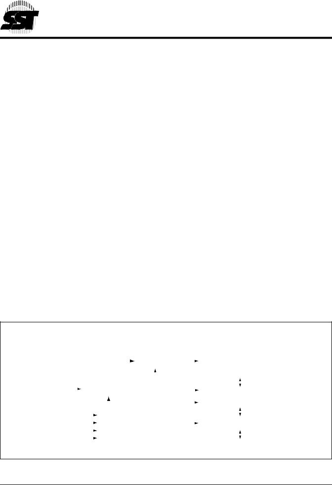
FUNCTIONAL BLOCK DIAGRAM |
|
|
|
|
|
|
|
|
|
|
|
|
|
|
|
|
||||
|
|
|
|
|
|
|
|
|
|
|
|
|
|
|
|
|
|
|
|
|
|
|
|
|
|
|
|
|
|
|
|
|
|
|
|
|
|
|
|
SuperFlash |
|
|
|
|
|
|
|
|
|
|
|
|
X-Decoder |
|
|
|
|
|||||
|
|
|
|
|
|
|
|
|
|
|
|
|
|
|
Memory |
|||||
|
|
|
|
|
|
|
|
|
|
|
|
|
|
|
|
|
|
|
||
Memory Address |
|
|
|
|
|
|
|
|
|
|
|
|
|
|
|
|
|
|
|
|
|
|
|
|
|
|
|
|
|
|
|
|
|
|
|
|
|
|
|
|
|
|
|
|
|
|
|
|
|
|
|
|
|
|
|
|
|
|
|
|
|
|
|
|
|
Address Buffer |
|
|
|
|
|
|
|
|
|
||||||||
|
|
|
|
|
|
|
|
|
|
|
|
|||||||||
CE# |
|
|
|
|
|
|
|
|
|
|
|
|
|
|
|
|
|
Y-Decoder |
||
|
|
|
|
|
|
|
|
|
|
|
|
|
|
|
|
|
||||
|
|
|
|
|
|
|
|
|
|
|
|
|
|
|
|
|
|
|
||
|
|
|
|
|
|
|
|
|
|
|
|
|
|
|
|
|
|
|
||
|
|
|
|
|
|
|
|
|
|
|
|
|
|
|
|
|
|
|||
|
|
|
|
|
|
|
|
|
|
|
|
|
|
|
|
|
|
|
||
|
|
|
|
|
|
|
|
|
|
|
|
|
|
|
|
|
|
|||
OE# |
|
|
|
|
|
|
Control Logic |
|
|
|
|
|
I/O Buffers |
|||||||
|
|
|
|
|
|
|
|
|
|
|
||||||||||
A9 |
|
|
|
|
|
|
|
|
|
|
|
|
|
|||||||
|
|
|
|
|
|
|
|
|
|
|
|
|
|
|
|
|
|
|||
|
|
|
|
|
|
|
|
|
|
|
|
|
|
|
|
|
|
|||
WE# |
|
|
|
|
|
|
|
|
|
|
|
|
|
|
|
|
|
|
||
|
|
|
|
|
|
|
|
|
|
|
|
|
|
|
|
DQ7 - DQ0 |
||||
|
|
|
|
|
|
|
|
|
|
|
|
|
|
|
|
|
|
|
||
|
|
|
|
|
|
|
|
|
|
|
|
|
|
|
|
|
|
|
||
397 ILL B1.1
©2001 Silicon Storage Technology, Inc. |
S71151-02-000 5/01 397 |
2

512 Kbit / 1 Mbit / 2 Mbit / 4 Mbit Multi-Purpose Flash SST37VF512 / SST37VF010 / SST37VF020 / SST37VF040
Data Sheet
SST37VF040 SST37VF020 SST37VF010 SST37VF512
A7 |
A7 |
A7 |
A7 |
A6 |
A6 |
A6 |
A6 |
A5 |
A5 |
A5 |
A5 |
A4 |
A4 |
A4 |
A4 |
A3 |
A3 |
A3 |
A3 |
A2 |
A2 |
A2 |
A2 |
A1 |
A1 |
A1 |
A1 |
A0 |
A0 |
A0 |
A0 |
DQ0 |
DQ0 |
DQ0 |
DQ0 |
SST37VF040 |
A12 |
|
A15 |
|
A16 |
|
A18 |
V |
|
WE# |
A17 |
||||
SST37VF020 |
|
|
|
|
|
|
|
|
DD |
|
|
|
|
|
|
A12 |
|
A15 |
|
A16 |
|
NC |
V |
|
WE# |
A17 |
|||||
SST37VF010 |
|
|
|
|
|
|
|
|
DD |
|
|
|
|
|
|
A12 |
|
A15 |
|
A16 |
|
NC |
V |
|
WE# |
NC |
|||||
SST37VF512 |
|
|
|
|
|
|
|
|
DD |
|
|
|
|
|
|
A12 |
|
A15 |
|
NC |
|
NC |
V |
|
WE# |
NC |
|||||
|
|
|
|
|
|
|
|
|
|
DD |
|
|
|
|
|
|
5 |
4 |
3 |
2 |
1 |
|
32 |
31 |
30 |
|
|||||
|
|
|
|
|
|
|
|
|
|
|
|
|
29 |
||
|
|
|
|
|
|
|
|
|
|
|
|
|
28 |
||
|
6 |
|
|
|
|
|
|
|
|
|
|
|
|
||
|
7 |
|
|
|
|
|
|
|
|
|
|
|
|
27 |
|
|
|
|
|
|
|
|
|
|
|
|
|
|
|||
|
8 |
|
|
32-pin PLCC |
26 |
||||||||||
|
|
|
|||||||||||||
|
9 |
|
|
25 |
|||||||||||
|
|
|
|||||||||||||
|
|
|
|
|
Top View |
|
|
|
|||||||
|
10 |
|
|
|
|
|
|
|
24 |
||||||
|
|
|
|
|
|
|
|
||||||||
|
|
|
|
|
|
|
|
|
|
|
|
|
|||
|
11 |
|
|
|
|
|
|
|
|
|
|
|
|
23 |
|
|
|
|
|
|
|
|
|
|
|
|
|
|
|||
|
12 |
|
|
|
|
|
|
|
|
|
|
|
|
22 |
|
|
|
|
|
|
|
|
|
|
|
|
|
|
|||
|
13 |
|
|
|
|
|
|
|
|
|
|
|
|
21 |
|
|
|
|
|
|
|
|
|
|
|
|
|
|
|||
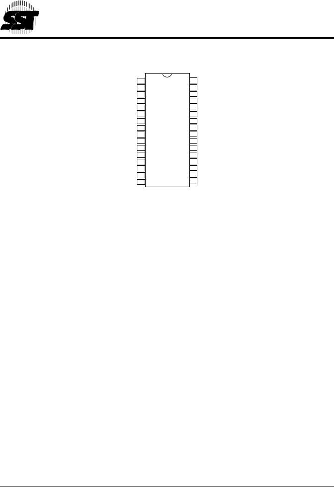
SST37VF512 |
14 |
15 |
16 |
17 |
18 |
19 |
|
20 |
|
||||||
|
|
|
|
|
|
|
|
|
|
|
|
|
|
||
|
|
|
|
|
|
|
|
|
|
|
|
|
|
||
DQ1 |
|
DQ2 |
|
V |
|
DQ3 |
DQ4 |
|
DQ5 |
DQ6 |
|||||
SST37VF010 |
|
|
|
|
SS |
|
|
|
|
|
|
|
|
|
|
DQ1 |
|
DQ2 |
|
V |
|
DQ3 |
DQ4 |
|
DQ5 |
DQ6 |
|||||
SST37VF020 |
|
|
|
|
SS |
|
|
|
|
|
|
|
|
|
|
DQ1 |
|
DQ2 |
|
V |
|
DQ3 |
DQ4 |
|
DQ5 |
DQ6 |
|||||
SST37VF040 |
|
|
|
|
SS |
|
|
|
|
|
|
|
|
|
|
DQ1 |
|
DQ2 |
|
V |
|
DQ3 |
DQ4 |
|
DQ5 |
DQ6 |
|||||
|
|
|
|
|
|
SS |
|
|
|
|
|
|
|
|
|
SST37VF512 SST37VF010 SST37VF020 SST37VF040
A14 |
A14 |
A14 |
A14 |
A13 |
A13 |
A13 |
A13 |
A8 |
A8 |
A8 |
A8 |
A9 |
A9 |
A9 |
A9 |
A11 |
A11 |
A11 |
A11 |
OE# |
OE# |
OE# |
OE# |
A10 |
A10 |
A10 |
A10 |
CE# |
CE# |
CE# |
CE# |
DQ7 |
DQ7 |
DQ7 |
DQ7 |
397 ILL F02a.2
FIGURE 1: PIN ASSIGNMENTS FOR 32-PIN PLCC
SST37VF040 SST37VF020 SST37VF010 SST37VF512
A11 |
A11 |
A11 |
A11 |
|
1 |
A9 |
A9 |
A9 |
A9 |
|
2 |
A8 |
A8 |
A8 |
A8 |
|
3 |
A13 |
A13 |
A13 |
A13 |
|
4 |
A14 |
A14 |
A14 |
A14 |
|
5 |
A17 |
A17 |
NC |
NC |
|
6 |
WE# |
WE# |
WE# |
WE# |
|
7 |
VDD |
VDD |
VDD |
VDD |
|
8 |
|
|||||
A18 |
NC |
NC |
NC |
|
9 |
A16 |
A16 |
A16 |
NC |
|
10 |
A15 |
A15 |
A15 |
A15 |
|
11 |
A12 |
A12 |
A12 |
A12 |
|
12 |
|
|||||
A7 |
A7 |
A7 |
A7 |
|
13 |
A6 |
A6 |
A6 |
A6 |
|
14 |
A5 |
A5 |
A5 |
A5 |
|
15 |
A4 |
A4 |
A4 |
A4 |
|
16 |
|
|||||
|
|
|
|
|
|
Standard Pinout
Top View
SST37VF512 SST37VF010 SST37VF020 SST37VF040
32 |
|
OE# |
OE# |
OE# |
OE# |
31 |
|
A10 |
A10 |
A10 |
A10 |
30 |
|
CE# |
CE# |
CE# |
CE# |
29 |
|
DQ7 |
DQ7 |
DQ7 |
DQ7 |
28 |
|
DQ6 |
DQ6 |
DQ6 |
DQ6 |
27 |
|
DQ5 |
DQ5 |
DQ5 |
DQ5 |
26 |
|
DQ4 |
DQ4 |
DQ4 |
DQ4 |
25 |
|
DQ3 |
DQ3 |
DQ3 |
DQ3 |
24 |
|
VSS |
VSS |
VSS |
VSS |
|
|||||
23 |
|
DQ2 |
DQ2 |
DQ2 |
DQ2 |
22 |
|
DQ1 |
DQ1 |
DQ1 |
DQ1 |
21 |
|
DQ0 |
DQ0 |
DQ0 |
DQ0 |
|
|||||
20 |
|
A0 |
A0 |
A0 |
A0 |
19 |
|
A1 |
A1 |
A1 |
A1 |
18 |
|
A2 |
A2 |
A2 |
A2 |
17 |
|
A3 |
A3 |
A3 |
A3 |
|
|||||
|
|
|
|
|
|
397 ILL F01.0
FIGURE 2: PIN ASSIGNMENTS FOR 32-PIN TSOP (8MM X 14MM)
©2001 Silicon Storage Technology, Inc. |
S71151-02-000 5/01 397 |
3
512 Kbit / 1 Mbit / 2 Mbit / 4 Mbit Multi-Purpose Flash SST37VF512 / SST37VF010 / SST37VF020 / SST37VF040
Data Sheet
|
SST37VF040 |
SST37VF020 SST37VF010 |
SST37VF512 |
|
|
|
SST37VF512 |
SST37VF010 |
SST37VF020 |
SST37VF040 |
|
|
A18 |
NC |
NC |
NC |
1 |
|
32 |
VDD |
VDD |
VDD |
VDD |
|
A16 |
A16 |
A16 |
NC |
2 |
|
31 |
WE# |
WE# |
WE# |
WE# |
|
A15 |
A15 |
A15 |
A15 |
3 |
|
30 |
NC |
NC |
A17 |
A17 |
|
A12 |
A12 |
A12 |
A12 |
4 |
|
29 |
A14 |
A14 |
A14 |
A14 |
|
A7 |
A7 |
A7 |
A7 |
5 |
32-pin |
28 |
A13 |
A13 |
A13 |
A13 |
|
A6 |
A6 |
A6 |
A6 |
6 |
27 |
A8 |
A8 |
A8 |
A8 |
|
|
|
||||||||||
|
A5 |
A5 |
A5 |
A5 |
7 |
PDIP |
26 |
A9 |
A9 |
A9 |
A9 |
|
A4 |
A4 |
A4 |
A4 |
8 |
Top View |
25 |
A11 |
A11 |
A11 |
A11 |
|
A3 |
A3 |
A3 |
A3 |
9 |
|
24 |
OE# |
OE# |
OE# |
OE# |
|
A2 |
A2 |
A2 |
A2 |
10 |
|
23 |
A10 |
A10 |
A10 |
A10 |
|
A1 |
A1 |
A1 |
A1 |
11 |
|
22 |
CE# |
CE# |
CE# |
CE# |
|
A0 |
A0 |
A0 |
A0 |
12 |
|
21 |
DQ7 |
DQ7 |
DQ7 |
DQ7 |
|
DQ0 |
DQ0 |
DQ0 |
DQ0 |
13 |
|
20 |
DQ6 |
DQ6 |
DQ6 |
DQ6 |
|
DQ1 |
DQ1 |
DQ1 |
DQ1 |
14 |
|
19 |
DQ5 |
DQ5 |
DQ5 |
DQ5 |
|
DQ2 |
DQ2 |
DQ2 |
DQ2 |
15 |
|
18 |
DQ4 |
DQ4 |
DQ4 |
DQ4 |
|
VSS |
VSS |
VSS |
VSS |
16 |
|
17 |
DQ3 |
DQ3 |
DQ3 |
DQ3 |
|
|
|
|
|
|
|
|
|
|
397 ILL F02b.1 |
|
|
|
|
|
|
|
|
|
||||
FIGURE |
3: PIN ASSIGNMENTS FOR 32-PIN PDIP |
|
|
|
|
|
|
||||
TABLE 2: PIN DESCRIPTION |
|
|
|
|
|
|
|
|
|
||
|
|
|
|
|
|
|
|
|
|
|
|
Symbol |
Pin Name |
|
Functions |
|
|
|
|
|
|
|
|
|
|
|
|
|
|
|
|
||||
AMS1-A0 |
Address Inputs |
To provide memory addresses. |
|
|
|
|
|
||||
DQ7-DQ0 |
Data Input/output |
To output data during Read cycles and receive input data during Program cycles. |
|||||||||
|
|
|
The outputs are in tri-state when OE# or CE# is high. |
|
|||||||
CE# |
Chip Enable |
|
To activate the device when CE# is low. |
|
|
|
|||||
WE# |
Write Enable |
|
To program or erase (WE# = VIL pulse during Program or Erase) |
||||||||
OE# |
Output Enable |
To gate the data output buffers during Read operation when low |
|||||||||
VDD |
Power Supply |
|
To provide 3.0V supply (2.7-3.6V) |
|
|
|
|
||||
VSS |
Ground |
|
|
|
|
|
|
|
|
|
|
NC |
No Connection |
Unconnected pins. |
|
|
|
|
|
|
|
||
|
|
|
|
|
|
|
|
|
|
|
|
T2.1 397
1.AMS = Most significant address
AMS = A15 for SST37VF512, A16 for SST37VF010, A17 for SST37VF020, and A18 for SST37VF040
©2001 Silicon Storage Technology, Inc. |
S71151-02-000 5/01 397 |
4

512 Kbit / 1 Mbit / 2 Mbit / 4 Mbit Multi-Purpose Flash SST37VF512 / SST37VF010 / SST37VF020 / SST37VF040
Data Sheet
TABLE 3: OPERATION MODES SELECTION
Mode |
CE# |
WE# |
A9 |
OE# |
DQ |
Address |
Read |
VIL |
VIH |
AIN |
VIL |
DOUT |
AIN |
Output Disable |
VIL |
X |
X |
VIH |
High Z |
AIN |
Standby |
VIH |
X |
X |
X |
High Z |
X |
Chip-Erase |
VIL |
VIL |
VH |
VH |
High Z |
X |
Byte-Program |
VIL |
VIL |
AIN |
VH |
DIN |
AIN |
Program/Erase Inhibit |
X |
VIH |
X |
X |
High Z |
X |
|
X |
X |
X |
VIL or VIH |
High Z/ DOUT |
X |
Product Identification |
VIL |
VIH |
VH |
VIL |
Manufacturer’s ID (BFH) |
AMS2 - A1 = VIL, A0 = VIL |
|
|
|
|
|
Device ID1 |
AMS2 - A1 = VIL, A0 = VIH |
T3.1 397
1.Device ID = C4H for SST37VF512, C5H for SST37VF020, C6H for SST37VF020, and C2H for SST37VF040
2.AMS = Most significant address
AMS = A15 for SST37VF512, A16 for SST37VF010, A17 for SST37VF020, and A18 for SST37VF040
Note: X = VIL or VIH (or VH in case of OE# and A9)
VH = 12V±5%
Absolute Maximum Stress Ratings (Applied conditions greater than those listed under “Absolute Maximum Stress Ratings” may cause permanent damage to the device. This is a stress rating only and functional operation of the device at these conditions or conditions greater than those defined in the operational sections of this data sheet is not implied. Exposure to absolute maximum stress rating conditions may affect device reliability.)
Temperature Under Bias . . . . . . . . . . . . . . . . . . . . . . . . . . . . . . . . . . . . . . . . . . . . . . . . . . . . . . . |
. . -55°C to +125°C |
Storage Temperature . . . . . . . . . . . . . . . . . . . . . . . . . . . . . . . . . . . . . . . . . . . . . . . . . . . . . . . . . |
. . -65°C to +150°C |
D. C. Voltage on Any Pin to Ground Potential . . . . . . . . . . . . . . . . . . . . . . . . . . . . . . . . . . . . . . . |
-0.5V to VDD + 0.5V |
Transient Voltage (<20 ns) on Any Pin to Ground Potential . . . . . . . . . . . . . . . . . . . . . . . . . . . . |
-1.0V to VDD + 1.0V |
Voltage on A9 Pin to Ground Potential . . . . . . . . . . . . . . . . . . . . . . . . . . . . . . . . . . . . . . . . . . . . |
. . . . -0.5V to 13.2V |
Package Power Dissipation Capability (Ta = 25°C) . . . . . . . . . . . . . . . . . . . . . . . . . . . . . . . . . . . |
. . . . . . . . . . . 1.0W |
Through Hold Lead Soldering Temperature (10 Seconds) . . . . . . . . . . . . . . . . . . . . . . . . . . . . . |
. . . . . . . . . . 300°C |
Surface Mount Lead Soldering Temperature (3 Seconds) . . . . . . . . . . . . . . . . . . . . . . . . . . . . . |
. . . . . . . . . . 240°C |
Output Short Circuit Current1 . . . . . . . . . . . . . . . . . . . . . . . . . . . . . . . . . . . . . . . . . . . . . . . . . . . |
. . . . . . . . . . 50 mA |
1. Outputs shorted for no more than one second. No more than one output shorted at a time.
OPERATING RANGE
Range |
Ambient Temp |
VDD |
Commercial |
0°C to +70°C |
2.7-3.6V |
|
|
|
AC CONDITIONS OF TEST
. . . . . . . . . . . . . . .Input Rise/Fall Time |
5 ns |
Output Load . . . . . . . . . . . . . . . . . . . . . |
CL = 100 pF |
See Figures 7 and 8 |
|
|
|
©2001 Silicon Storage Technology, Inc. |
S71151-02-000 5/01 397 |
5
 Loading...