


Silicon Storage Technology Inc SST30VR022-70-C-WN-R, SST30VR022-70-C-WH-R, SST30VR022-70-C-UN-R, SST30VR022-70-C-UH-R, SST30VR022-500-E-WH-R Datasheet
...
2 Mbit ROM + 1 Mbit / 2Mbit / 256 Kbit SRAM
ROM/RAM Combo
SST30VR021 / SST30VR022 / SST30VR023
FEATURES:
•ROM + SRAM ROM/RAM Combo
–SST30VR021: 256K x8 ROM + 128K x8 SRAM
–SST30VR022: 256K x8 ROM + 256K x8 SRAM
– SST30VR023: 256K x8 ROM + 32K x8 SRAM
•ROM/RAM combo on a monolithic chip
•Equivalent ComboMemory (Flash + SRAM): SST31LF021E for code development and pre-production
•Wide Operating Voltage Range: 2.7-3.3V
•Chip Access Time
– |
SST30VR022 |
70 ns |
– |
SST30VR021/023 |
500 ns |
Data Sheet
•Low Power Dissipation:
–Standby: 3 µW (Typical)
–Operating: 10 mW (Typical)
•Fully Static Operation
–No clock or refresh required
•Three state Outputs
•Packages Available
–32-pin TSOP (8mm x14mm)
PRODUCT DESCRIPTION
The SST30VR021/022/023 are ROM/RAM combo chips consisting of 2 Mbit Read Only Memory organized as 256 KBytes and Static Random Access Memory organized as 128, 256, and 32 KBytes.
The device is fabricated using SST’s advanced CMOS low power process technology.
The SST30VR021/022/023 has an output enable input for precise control of the data outputs. It also has two (2) separate chip enable inputs for selection of either RAM or ROM and for minimizing current drain during power-down mode.
The SST30VR021/022/023 is particularly well suited for use in low voltage (2.7-3.3V) supplies such as pagers, organizers and other handheld applications.
FUNCTIONAL BLOCK DIAGRAM
RAMCS#
ROMCS#
OE#
WE#
AMS-A0
Control |
Circuit |
Address Buffer
RAMCS#
OE#
WE#
RAM
ROMCS#
OE#
ROM
Data Buffer
DQ7-DQ0
Note: AMS = Most Significant Address |
380 ILL B1.1 |
|
©2001 Silicon Storage Technology, Inc. |
The SST logo and SuperFlash are registered trademarks of Silicon Storage Technology, Inc. |
|
S71135-02-000 4/01 |
380 |
ComboMemory is a trademark of Silicon Storage Technology, Inc. |
|
|
These specifications are subject to change without notice. |
2 Mbit ROM + 1 Mbit / 2Mbit / 256 Kbit SRAM ROM/RAM Combo SST30VR021 / SST30VR022 / SST30VR023
Data Sheet
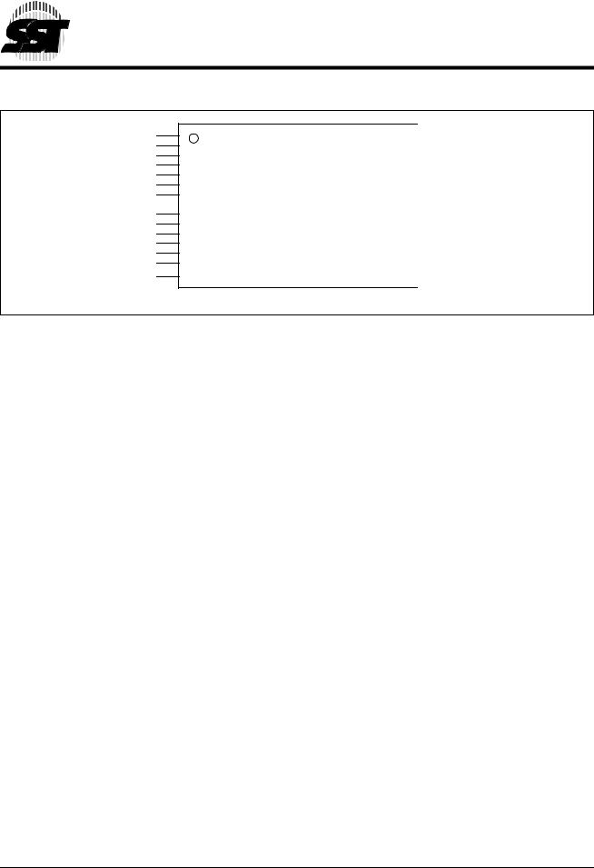
A11  1
1
A9  2
2
A8  3
3
A13  4
4
A14  5
5
A17  6 RAMCS#
  7
7
VDD  8
8
WE#  9
9
A16  10
10
A15  11
11
A12  12
12
A7  13
13
A6  14
14
A5  15
15
A4  16
16
|
32 |
|
|
OE# |
|
31 |
|
|
A10 |
|
30 |
|
|
ROMCS# |
|
29 |
|
|
DQ7 |
Standard Pinout |
28 |
|
|
DQ6 |
27 |
|
|
DQ5 |
|
Top View |
26 |
|
|
DQ4 |
25 |
|
|
DQ3 |
|
Die Up |
24 |
|
|
VSS |
|
|
|||
23 |
|
|
DQ2 |
|
|
22 |
|
|
DQ1 |
|
21 |
|
|
DQ0 |
|
20 |
|
|
A0 |
|
19 |
|
|
A1 |
|
18 |
|
|
A2 |
|
17 |
|
|
A3 |
|
|
|
|
|
380 ILL F01.0
FIGURE 1: PIN ASSIGNMENTS FOR 32-PIN TSOP
TABLE |
1: PIN DESCRIPTION |
|
Symbol |
|
Pin Name |
|
|
|
AMS1-A0 |
|
Address Inputs, for ROM: AMS = A17, for RAM: AMS =A16 for SST30VR021 |
|
|
A17 for SST30VR022 |
|
|
A14 for SST30VR023 |
WE# |
|
Write Enable Input |
OE# |
|
Output Enable |
RAMCS# |
|
RAM Enable Input |
ROMCS# |
|
ROM Enable Input |
DQ7-DQ0 |
|
Data Input/Output |
VDD |
|
Power Supply |
VSS |
|
Ground |
|
|
T1.2 380 |
1. AMS = Most significant address
©2001 Silicon Storage Technology, Inc. |
S71135-02-000 4/01 380 |
2

2 Mbit ROM + 1 Mbit / 2Mbit / 256 Kbit SRAM ROM/RAM Combo
SST30VR021 / SST30VR022 / SST30VR023
Data Sheet
Absolute Maximum Stress Ratings (Applied conditions greater than those listed under “Absolute Maximum Stress Ratings” may cause permanent damage to the device. This is a stress rating only and functional operation of the device at these conditions or conditions greater than those defined in the operational sections of this data sheet is not implied. Exposure to absolute maximum stress rating conditions may affect device reliability.)
Operating Temperature . . . . . . . . . . . . . . . . . . . . . . . . . . . . . . . . . . . . . . . . . . . . . . . . . . . . . . . . . . . -20°C to +85°C Storage Temperature . . . . . . . . . . . . . . . . . . . . . . . . . . . . . . . . . . . . . . . . . . . . . . . . . . . . . . . . . . . -65°C to +150°C Voltage on Any Pin Relative to VSS . . . . . . . . . . . . . . . . . . . . . . . . . . . . . . . . . . . . . . . . . . . . . . . -0.5V to VDD + 0.5V Voltage on VDD Supply Relative to VSS . . . . . . . . . . . . . . . . . . . . . . . . . . . . . . . . . . . . . . . . . . . . . . . . . -0.5V to 4.0V Power Dissipation. . . . . . . . . . . . . . . . . . . . . . . . . . . . . . . . . . . . . . . . . . . . . . . . . . . . . . . . . . . . . . . . . . . . . . . . 1.0W Soldering Temperature (10 Seconds Lead Only) . . . . . . . . . . . . . . . . . . . . . . . . . . . . . . . . . . . . . . . . . . . . . . 260°C
OPERATING RANGE |
|
|
|
|
|
|
|
|
|
|
|
|
|
|
|
|||
Range |
|
|
|
Ambient Temp |
|
|
VDD |
|
|
|
|
|
|
|
|
|
|
|
Commercial |
|
|
0°C to +70°C |
|
2.7-3.3V |
|
|
|
|
|
|
|
|
|
|
|||
Extended |
|
|
|
-20°C to +85°C |
|
2.7-3.3V |
|
|
|
|
|
|
|
|
|
|
||
|
|
|
|
|
|
|
|
|
|
|
|
|
|
|
|
|
|
|
AC CONDITIONS OF TEST |
|
|
|
|
|
|
|
|
|
|
|
|
|
|||||
|
|
|
|
|
|
|
|
|
|
|
|
|
|
|
|
|||
Input Pulse Level . . . . |
. . . . . . . . . . . . . . . . |
. . |
. |
.0-VDD |
|
|
|
|
|
|
|
|||||||
Input & Output Timing Reference Levels . . . . . |
. |
.VDD/2 |
|
|
|
|
|
|
|
|
|
|
||||||
Input Rise/Fall Time . |
. . . . . . . . . . . . . . . . . . |
. . |
. |
. 5 ns |
|
|
|
|
|
|
|
|
|
|
||||
Output Load . . . . . . . |
. . . . . . . . . . . . . . . . . . |
. . |
. |
. CL = 30 pF for |
70 ns |
|
|
|
|
|
||||||||
Output Load . . . . . . . |
. . . . . . . . . . . . . . . . . . |
. . |
. |
. CL = 100 pF for 500 ns |
|
|
|
|
|
|||||||||
TABLE |
2: RECOMMENDED DC OPERATING CONDITIONS |
|
|
|
|
|
|
|
||||||||||
|
|
|
|
|
|
|
|
|
|
|
|
|
|
|
|
|||
Symbol |
|
Parameter |
|
|
|
|
|
|
Min |
|
Max |
|
Units |
|||||
|
|
|
|
|
|
|
|
|
|
|
|
|
|
|
|
|
||
VDD |
|
Supply Voltage |
|
|
|
|
|
|
2.7 |
|
|
3.3 |
|
V |
||||
VSS |
|
Ground |
|
|
|
|
|
|
0 |
|
|
0 |
|
V |
||||
VIH |
|
Input High Voltage |
|
|
|
|
|
2.4 |
|
|
VDD + 0.5 |
|
V |
|||||
VIL |
|
Input Low Voltage |
|
|
|
|
|
-0.3 |
|
|
0.3 |
|
V |
|||||
|
|
|
|
|
|
|
|
|
|
|
|
|
|
|
|
|
|
T2.0 380 |
TABLE |
3: DC OPERATING CHARACTERISTICS |
|
|
|
|
|
|
|
|
|
|
|||||||
|
|
|
|
|
|
|
|
|
|
|
|
|
|
|||||
|
|
|
|
|
|
|
VDD = 3.0 ± 0.3V |
|
|
|
|
|||||||
Symbol |
Parameter |
|
|
|
Min |
|
|
|
Max |
|
Units |
Test Conditions |
|
|||||
|
|
|
|
|
|
|
|
|||||||||||
IDD1 |
ROM Operating Supply Current |
|
|
4.0+1.1(f)1 |
|
mA |
ROMCS#=VIL, RAMCS#=VIH, |
|||||||||||
|
|
|
|
|
|
|
|
|
|
|
|
|
|
|
VIN=VIH or VIL, II/O=Opens |
|
||
IDD2 |
RAM Operating Supply Current |
|
|
|
2.5+1(f)1 |
|
mA |
ROMCS#=VIH, RAMCS#=VIL, II/O=Opens |
||||||||||
ISB |
Standby VDD Current |
|
|
|
10 |
|
µA |
ROMCS#≥ VDD-0.2V, RAMCS#≥ VDD-0.2V |
||||||||||
|
|
|
|
|
|
|
|
|
|
|
|
|
|
|
VIN≥ VDD-0.2V or VIN ≤ 0.2V |
|
||
ILI |
Input Leakage Current |
|
-1 |
|
1 |
|
µA |
VIN=VSS to VDD |
|
|||||||||
ILO |
Output Leakage Current |
|
-1 |
|
1 |
|
µA |
ROMCS#=RAMCS#=VIH or OE#=VIH or |
||||||||||
|
|
|
|
|
|
|
|
|
|
|
|
|
|
|
WE#=VIL, VI/O=VSS to VDD |
|
||
VOL |
Output Low Voltage |
|
|
|
0.4 |
|
V |
IOL = 1.0 mA |
|
|||||||||
VOH |
Output High Voltage |
|
2.2 |
|
|
|
|
|
V |
IOH = -0.5 mA |
|
|||||||
1. f = Frequency of operation (MHz) = 1/cycle time |
|
|
|
|
|
|
|
|
|
|
|
|
T3.3 380 |
|||||
|
|
|
|
|
|
|
|
|
|
|
|
|
||||||
|
|
|
|
|
|
|
|
|
|
|
|
|
|
|
|
|
|
|
©2001 Silicon Storage Technology, Inc. |
|
|
|
3 |
|
|
|
|
|
|
S71135-02-000 4/01 380 |
|||||||
|
|
|
|
|
|
|
|
|
|
|
|
|
|
|
|
|||
2 Mbit ROM + 1 Mbit / 2Mbit / 256 Kbit SRAM ROM/RAM Combo SST30VR021 / SST30VR022 / SST30VR023
Data Sheet
TABLE 4: CAPACITANCE (Ta = 25°C, f=1 Mhz)
Parameter |
Description |
Test Condition |
Maximum |
|
|
|
|
CI/O1 |
I/O Pin Capacitance |
VI/O = 0V |
8 pF |
CIN1 |
Input Capacitance |
VIN = 0V |
6 pF |
T4.1 380
1. This parameter is measured only for initial qualification and after a design or process change that could affect this parameter.
VIHT
INPUT |
|
VIT |
|
REFERENCE POINTS |
|
VOT |
|
OUTPUT |
|
|
|
|
|||||
VILT |
|
|
|
|
|
|
|
|
|
|
|
|
|
|
|
|
380 ILL F08.0 |
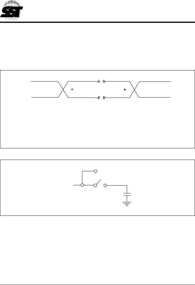
AC test inputs are driven at VIHT (0.9 VDD) for a logic “1” and VILT (0.1 VDD) for a logic “0”. Measurement reference points |
|
for inputs and outputs are VIT (0.5 VDD) and VOT (0.5 VDD). Input rise and fall times (10% ↔ |
90%) are <5 ns. |
Note: VIT - VINPUT Test
VOT - VOUTPUT Test
VIHT - VINPUT HIGH Test
VILT - VINPUT LOW Test
FIGURE 2: AC INPUT/OUTPUT REFERENCE WAVEFORMS
TO TESTER
TO DUT
CL
380 ILL F09.0
FIGURE 3: A TEST LOAD EXAMPLE
©2001 Silicon Storage Technology, Inc. |
S71135-02-000 4/01 380 |
4
 Loading...