


Silicon Storage Technology Inc SST28VF040A-90-4I-WH, SST28VF040A-90-4I-PH, SST28VF040A-90-4I-NH, SST28VF040A-90-4I-EH, SST28VF040A-90-4C-WH Datasheet
...4 Mbit (512K x8) SuperFlash EEPROM
SST28SF040A / SST28VF040A
FEATURES:
•Single Voltage Read and Write Operations
–5.0V-only for SST28SF040A
–2.7-3.6V for SST28VF040A
•Superior Reliability
–Endurance: 100,000 Cycles (typical)
–Greater than 100 years Data Retention
•Memory Organization: 512K x8
•Sector-Erase Capability: 256 Bytes per Sector
•Low Power Consumption
–Active Current: 15 mA (typical) for 5.0V and 10 mA (typical) for 2.7-3.6V
–Standby Current: 5 µA (typical)
•Fast Sector-Erase/Byte-Program Operation
–Byte-Program Time: 35 µs (typical)
–Sector-Erase Time: 2 ms (typical)
–Complete Memory Rewrite: 20 sec (typical)
Data Sheet
•Fast Read Access Time
–5.0V-only operation: 90 and 120 ns
–2.7-3.6V operation: 150 and 200 ns
•Latched Address and Data
•Hardware and Software Data Protection
–7-Read-Cycle-Sequence Software Data Protection
•End-of-Write Detection
–Toggle Bit
–Data# Polling
•TTL I/O Compatibility
•JEDEC Standard
–Flash EEPROM Pinouts
•Packages Available
–32-lead PLCC
–32-lead TSOP (8mm x 14mm and 8mm x 20mm)
–32-pin PDIP
PRODUCT DESCRIPTION
The SST28SF/VF040A are 512K x8 bit CMOS SectorErase, Byte-Program EEPROMs. The SST28SF/VF040A are manufactured using SST’s proprietary, high performance CMOS SuperFlash EEPROM Technology. The split-gate cell design and thick oxide tunneling injector attain better reliability and manufacturability compared with alternative approaches. The SST28SF/VF040A erase and program with a single power supply. The SST28SF/ VF040A conform to JEDEC standard pinouts for byte wide memories and are compatible with existing industry standard flash EEPROM pinouts.
Featuring high performance programming, the SST28SF/ VF040A typically Byte-Program in 35 µs. The SST28SF/ VF040A typically Sector-Erase in 2 ms. Both Program and Erase times can be optimized using interface features such as Toggle bit or Data# Polling to indicate the completion of the Write cycle. To protect against an inadvertent write, the SST28SF/VF040A have on chip hardware and Software Data Protection schemes. Designed, manufactured, and tested for a wide spectrum of applications, the SST28SF/ VF040A are offered with a guaranteed sector endurance of 10,000 cycles. Data retention is rated greater than 100 years.
The SST28SF/VF040A are best suited for applications that require reprogrammable nonvolatile mass storage of program, configuration, or data memory. For all system appli-
cations, the SST28SF/VF040A significantly improve performance and reliability, while lowering power consumption when compared with floppy diskettes or EPROM approaches. Flash EEPROM technology makes possible convenient and economical updating of codes and control programs on-line. The SST28SF/VF040A improve flexibility, while lowering the cost of program and configuration storage application.
The functional block diagram shows the functional blocks of the SST28SF/VF040A. Figures 1, 2, and 3 show the pin assignments for the 32-lead PLCC, 32-lead TSOP, and 32pin PDIP packages. Pin descriptions and operation modes are described in Tables 2 through 5.
Device Operation
Commands are used to initiate the memory operation functions of the device. Commands are written to the device using standard microprocessor write sequences. A command is written by asserting WE# low while keeping CE# low. The address bus is latched on the falling edge of WE# or CE#, whichever occurs last. The data bus is latched on the rising edge of WE# or CE#, whichever occurs first. Note, during the Software Data Protection sequence the addresses are latched on the rising edge of OE# or CE#, whichever occurs first.
©2001 Silicon Storage Technology, Inc. |
The SST logo and SuperFlash are registered trademarks of Silicon Storage Technology, Inc. |
|
S71077-04-000 6/01 |
310 |
SSF is a trademark of Silicon Storage Technology, Inc. |
|
|
These specifications are subject to change without notice. |

4 Mbit SuperFlash EEPROM
SST28SF040A / SST28VF040A
Command Definitions
Table 4 contains a command list and a brief summary of the commands. The following is a detailed description of the operations initiated by each command.
Sector-Erase Operation
The Sector-Erase operation erases all bytes within a sector and is initiated by a setup command and an execute command. A sector contains 256 Bytes. This sector erasability enhances the flexibility and usefulness of the SST28SF/ VF040A, since most applications only need to change a small number of bytes or sectors, not the entire chip.
The setup command is performed by writing 20H to the device. The execute command is performed by writing D0H to the device. The Erase operation begins with the rising edge of the WE# or CE#, whichever occurs first and terminates automatically by using an internal timer. The End-of- Erase can be determined using either Data# Polling, Toggle Bit, or Successive Reads detection methods. See Figure 9 for timing waveforms.
The two-step sequence of a setup command followed by an execute command ensures that only memory contents within the addressed sector are erased and other sectors are not inadvertently erased.
Sector-Erase Flowchart Description
Fast and reliable erasing of the memory contents within a sector is accomplished by following the Sector-Erase flowchart as shown in Figure 18. The entire procedure consists of the execution of two commands. The Sector-Erase operation will terminate after a maximum of 4 ms. A Reset command can be executed to terminate the Sector-Erase operation; however, if the Erase operation is terminated prior to the 4 ms time-out, the sector may not be fully erased. A Sector-Erase command can be reissued as many times as necessary to complete the Erase operation. The SST28SF/VF040A cannot be over-erased.
Chip-Erase Operation
The Chip-Erase operation is initiated by a setup command (30H) and an execute command (30H). The Chip-Erase operation allows the entire array of the SST28SF/VF040A to be erased in one operation, as opposed to 2048 SectorErase operations. Using the Chip-Erase operation will minimize the time to rewrite the entire memory array. The ChipErase operation will terminate after a maximum of 20 ms. A Reset command can be executed to terminate the Erase operation; however, if the Chip-Erase operation is terminated prior to the 20 ms time-out, the chip may not be completely erased. If an erase error occurs a Chip-Erase
Data Sheet
command can be reissued as many times as necessary to complete the Chip-Erase operation. The SST28SF/ VF040A cannot be over-erased. (See Figure 8)
Byte-Program Operation
The Byte-Program operation is initiated by writing the setup command (10H). Once the program setup is performed, programming is executed by the next WE# pulse. See Figures 5 and 6 for timing waveforms. The address bus is latched on the falling edge of WE# or CE#, whichever occurs last. The data bus is latched on the rising edge of WE# or CE#, whichever occurs first, and begins the Program operation. The Program operation is terminated automatically by an internal timer. See Figure 16 for the programming flowchart.
The two-step sequence of a setup command followed by an execute command ensures that only the addressed byte is programmed and other bytes are not inadvertently programmed.
The Byte-Program Flowchart Description
Programming data into the SST28SF/VF040A is accomplished by following the Byte-Program flowchart shown in Figure 16. The Byte-Program command sets up the byte for programming. The address bus is latched on the falling edge of WE# or CE#, whichever occurs last. The data bus is latched on the rising edge of WE# or CE#, whichever occurs first and begins the Program operation. The end of program can be detected using either the Data# Polling, Toggle bit, or Successive reads.
Reset Operation
The Reset command is provided as a means to safely abort the Erase or Program command sequences. Following either setup commands (Erase or Program) with a write of FFH will safely abort the operation. Memory contents will not be altered. After the Reset command, the device returns to the Read mode. The Reset command does not enable Software Data Protection. See Figure 7 for timing waveforms.
Read
The Read operation is initiated by setting CE#, and OE# to logic low and setting WE# to logic high (See Table 3). See Figure 4 for Read cycle timing waveform. The Read operation from the host retrieves data from the array. The device remains enabled for Read until another operation mode is accessed. During initial power-up, the device is in the Read mode and is Software Data protected. The device must be unprotected to execute a Write command.
©2001 Silicon Storage Technology, Inc. |
S71077-04-000 6/01 310 |
2

4 Mbit SuperFlash EEPROM
SST28SF040A / SST28VF040A
Data Sheet
The Read operation of the SST28SF/VF040A are controlled by OE# and CE# at logic low. When CE # is high, the chip is deselected and only standby power will be consumed. OE# is the output control and is used to gate data from the output pins. The data bus is in high impedance state when CE# or OE# are high.
rising edge of OE# or CE#, whichever occurs first. A similar seven read sequence of 1823H, 1820H, 1822H, 0418H, 041BH, 0419H, 040AH will protect the device. Also refer to Figures 10 and 11 for the 7 read cycle sequence Software Data Protection. The I/O pins can be in any state (i.e., high, low, or tri-state).
Read-ID operation
The Read-ID operation is initiated by writing a single command (90H). A read of address 0000H will output the manufacturer’s ID (BFH). A read of address 0001H will output the device ID (04H). Any other valid command will terminate this operation.
Data Protection
In order to protect the integrity of nonvolatile data storage, the SST28SF/VF040A provide both
hardware and software features to prevent inadvertent writes to the device, for example, during system power-up or power-down. Such provisions are described below.
Hardware Data Protection
The SST28SF/VF040A are designed with hardware features to prevent inadvertent writes. This is done in the following ways:
1.Write Cycle Inhibit Mode: OE# low, CE#, or WE# high will inhibit the Write operation.
2.Noise/Glitch Protection: A WE# pulse width of less than 5 ns will not initiate a Write cycle.
3.VDD Power Up/Down Detection: The Write operation is inhibited when VDD is less than 2.0V.
4.After power-up, the device is in the Read mode and the device is in the Software Data Protect state.
Write Operation Status Detection
The SST28SF/VF040A provide three means to detect the completion of a Write operation, in order to optimize the system Write operation. The end of a Write operation (Erase or Program) can be detected by three means: 1) monitoring the Data# Polling bit, 2) monitoring the Toggle bit, or 3) by two successive reads of the same data. These three detection mechanisms are described below.
The actual completion of the nonvolatile Write is asynchronous with the system; therefore, either a Data# Polling or Toggle Bit read may be simultaneous with the completion of the Write cycle. If this occurs, the system may possibly get an erroneous result, i.e., valid data may appear to conflict with the DQ used. In order to prevent spurious rejection, if an erroneous result occurs, the software routine should include a loop to read the accessed location an additional two (2) times. If both reads are valid, then the device has completed the Write cycle, otherwise the rejection is valid.
Data# Polling (DQ7)
The SST28SF/VF040A feature Data# Polling to indicate the Write operation status. During a Write operation, any attempt to read the last byte loaded during the byte-load cycle will receive the complement of the true data on DQ7. Once the Write cycle is completed, DQ7 will show true data. The device is then ready for the next operation. See Figure 12 for Data# Polling timing waveforms. In order for Data# Polling to function correctly, the byte being polled must be erased prior to programming.
Software Data Protection (SDP)
The SST28SF/VF040A have software methods to further prevent inadvertent writes. In order to perform an Erase or Program operation, a two-step command sequence consisting of a set-up command followed by an execute command avoids inadvertent erasing and programming of the device.
The SST28SF/VF040A will default to Software Data Protection after power up. A sequence of seven consecutive reads at specific addresses will unprotect the device The address sequence is 1823H, 1820H, 1822H, 0418H, 041BH, 0419H, 041AH. The address bus is latched on the
Toggle Bit (DQ6)
An alternative means for determining the Write operation status is by monitoring the Toggle Bit, DQ6. During a Write operation, consecutive attempts to read data from the device will result in DQ6 toggling between logic 0 (low) and logic 1 (high). When the Write cycle is completed, the toggling will stop. The device is then ready for the next operation. See Figure 13 for Toggle Bit timing waveforms.
©2001 Silicon Storage Technology, Inc. |
S71077-04-000 6/01 310 |
3

4 Mbit SuperFlash EEPROM
SST28SF040A / SST28VF040A
Successive Reads
An Alternative means for determining an end of a write operation is by reading the same address for two consecutive data matches.
Product Identification
The Product Identification mode identifies the device as SST28SF/VF040A and the manufacturer as SST. This mode may be accessed by hardware and software operations. The hardware operation is typically used by an external programmer to identify the correct algorithm for the
Data Sheet
SST28SF/VF040A. Users may wish to use the software operation to identify the device (i.e., using the device ID). For details see Table 3 for the hardware operation and Figure 19 for the software operation. The manufacturer and device IDs are the same for both operations.
TABLE 1: PRODUCT IDENTIFICATION
|
Address |
Data |
|
|
|
Manufacturer’s ID |
0000H |
BFH |
|
|
|
Device ID |
|
|
SST28SF/VF040A |
0001H |
04H |
|
|
|
T1.1 310
FUNCTIONAL BLOCK DIAGRAM
|
|
|
|
|
|
|
|
|
|
|
|
|
|
|
|
|
|
SuperFlash |
|
|
|
|
|
|
|
|
|
|
|
X-Decoder |
|
|
|
|
|||||
|
|
|
|
|
|
|
|
|
|
|
|
|
|
Memory |
|||||
|
|
|
|
|
|
|
|
|
|
|
|
|
|
||||||
|
|
|
|
|
|
|
|
|
|
|
|
|
|
|
|
|
|
||
A18 - A0 |
|
|
|
|
|
|
|
|
|
|
|
|
|
|
|
|
|
|
|
|
|
|
|
|
|
|
|
|
|
|
|
|
|
|
|
|
|
|
|
|
|
|
|
|
|
|
|
|
|
|
|
|
|
|
|
|
|
|
|
|
|
Address Buffer & Latches |
|
|
|
|
|
|
|
|
|
||||||||
|
|
|
|
|
|
|
|
|
|
|
|||||||||
CE# |
|
|
|
|
|
|
|
|
|
|
|
|
|
|
|
|
Y-Decoder |
||
|
|
|
|
|
|
|
|
|
|
|
|
|
|
|
|
||||
|
|
|
|
|
|
|
|
|
|
|
|
|
|
|
|
||||
|
|
|
|
|
|
|
|
|
|
|
|
|
|
|
|
|
|
||
|
|
|
|
|
|
|
|
|
|
|
|
|
|
|
|
|
|
||
|
|
|
|
|
|
|
|
|
|
|
|
|
|
|
|
|
|
||
|
|
|
|
Control Logic |
|
|
|
|
|
|
|
||||||||
OE# |
|
|
|
|
|
|
|
|
|
|
|
||||||||
|
|
|
|
|
|
|
|
I/O Buffers and Data Latches |
|||||||||||
|
|
|
|
|
|
|
|
|
|||||||||||
WE# |
|
|
|
|
|
|
|
|
|
|
|
|
|
|
|
|
|
|
|
|
|
|
|
|
|
|
|
|
|
|
|
|
|
|
|
||||
|
|
|
|
|
|
|
|
|
|
|
|
|
|
|
|
|
|
||
|
|
|
|
|
|
|
|
|
|
|
|
|
|
|
|
|
|
|
|
|
|
|
|
|
|
|
|
|
|
|
|
|
|
|
|
|
|
DQ7 - DQ0 |
|
310 ILL B1.1
|
|
A12 |
|
A15 |
|
A16 |
|
A18 |
DD |
|
WE# |
A17 |
|
|||
|
|
|
|
|
V |
|
|
|||||||||
|
4 |
3 |
2 |
1 |
|
32 |
31 |
30 |
|
|
||||||
A7 |
5 |
|
|
|
|
|
|
|
|
|
|
|
|
29 |
A14 |
|
A6 |
6 |
|
|
|
|
|
|
|
|
|
|
|
|
28 |
A13 |
|
A5 |
7 |
|
|
|
|
|
|
|
|
|
|
|
|
27 |
A8 |
|
A4 |
8 |
|
|
32-lead PLCC |
26 |
A9 |
||||||||||
A3 |
9 |
|
|
25 |
A11 |
|||||||||||
|
|
|
|
Top View |
|
|
|
|||||||||
A2 |
10 |
|
|
|
|
|
|
|
24 |
OE# |
||||||
|
|
|
|
|
|
|
|
|
|
|
|
|||||
A1 |
11 |
|
|
|
|
|
|
|
|
|
|
|
|
23 |
A10 |
|
A0 |
12 |
|
|
|
|
|
|
|
|
|
|
|
|
22 |
CE# |
|
DQ0 |
13 |
|
|
|
|
|
|
|
|
|
|
|
|
21 |
DQ7 |
|
|
14 |
15 |
16 |
17 |
18 |
19 |
|
20 |
|
|
||||||
|
|
|
|
|
|
|
|
|
|
|
|
|
|
|
|
|
DQ1 |
DQ2 |
SS |
DQ3 |
DQ4 |
DQ5 |
DQ6 |
V |
310 ILL F02.3
FIGURE 1: PIN ASSIGNMENTS FOR 32-LEAD PLCC
©2001 Silicon Storage Technology, Inc. |
S71077-04-000 6/01 310 |
4
4 Mbit SuperFlash EEPROM
SST28SF040A / SST28VF040A
Data Sheet
A11  1
1
A9  2
2
A8  3
3
A13  4
4
A14  5
5
A17  6 WE#
6 WE#  7
7
VDD  8 A18
8 A18  9
9
A16  10
10
A15  11
11
A12  12
12
A7  13
13
A6  14
14
A5  15
15
A4  16
16
|
32 |
|
OE# |
|
31 |
|
A10 |
|
30 |
|
CE# |
|
29 |
|
DQ7 |
Standard Pinout |
28 |
|
DQ6 |
27 |
|
DQ5 |
|
Top View |
26 |
|
DQ4 |
25 |
|
DQ3 |
|
Die Up |
24 |
|
VSS |
|
|||
23 |
|
DQ2 |
|
|
22 |
|
DQ1 |
|
21 |
|
DQ0 |
|
20 |
|
A0 |
|
19 |
|
A1 |
|
18 |
|
A2 |
|
17 |
|
A3 |
|
|
|
|
310 ILL F01.2
FIGURE |
2: PIN ASSIGNMENTS FOR 32-LEAD TSOP |
|
|
||||
|
|
|
|
|
|
|
|
|
|
|
A18 |
1 |
|
32 |
VDD |
|
|
|
A16 |
2 |
|
31 |
WE# |
|
|
|
A15 |
3 |
|
30 |
A17 |
|
|
|
A12 |
4 |
|
29 |
A14 |
|
|
|
A7 |
5 |
32-pin |
28 |
A13 |
|
|
|
A6 |
6 |
27 |
A8 |
|
|
|
|
|
||||
|
|
|
A5 |
7 |
PDIP |
26 |
A9 |
|
|
|
A4 |
8 |
Top View |
25 |
A11 |
|
|
|
A3 |
9 |
|
24 |
OE# |
|
|
|
A2 |
10 |
|
23 |
A10 |
|
|
|
A1 |
11 |
|
22 |
CE# |
|
|
|
A0 |
12 |
|
21 |
DQ7 |
|
|
|
DQ0 |
13 |
|
20 |
DQ6 |
|
|
|
DQ1 |
14 |
|
19 |
DQ5 |
|
|
|
DQ2 |
15 |
|
18 |
DQ4 |
|
|
|
VSS |
16 |
|
17 |
DQ3 |
|
|
|
|
|
|
|
310 ILL F19.0 |
|
|
|
|
|
|
|
|
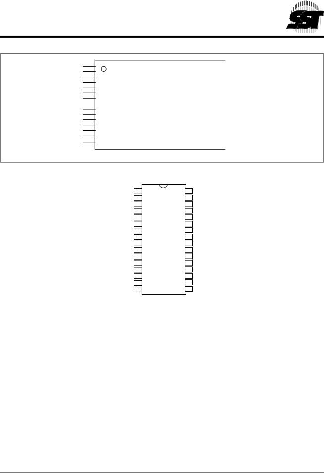
FIGURE |
3: PIN ASSIGNMENTS FOR 32-PIN PDIP |
|
|
|
|||
TABLE 2: PIN DESCRIPTION |
|
|
|
|
|
||
|
|
|
|
|
|
|
|
Symbol |
|
Pin Name |
Functions |
|
|
|
|
|
|
|
|
||||
A18-A8 |
|
Row Address Inputs |
To provide memory addresses. Row addresses define a sector. |
||||
A7-A0 |
|
Column Address Inputs |
Selects the byte within the sector |
|
|||
DQ7-DQ0 |
|
Data Input/output |
To output data during Read cycles and receive input data during Write cycles. |
||||
|
|
|
Data is internally latched during a Write cycle. |
||||
|
|
|
The outputs are in tri-state when OE# or CE# is high. |
||||
CE# |
|
Chip Enable |
To activate the device when CE# is low.1 |
||||
OE# |
|
Output Enable |
To gate the data output buffers. |
|
|||
WE# |
|
Write Enable |
To control the Write operations.1 |
|
|||
VDD |
|
Power Supply |
To provide: |
5.0V supply (±10%) for SST28SF040A |
|||
|
|
|
|
2.7V supply (2.7-3.6V) for SST28VF040A |
|||
VSS |
|
Ground |
|
|
|
|
|
T2.2 310
1. This pin is internally pull-up with a resistor.
©2001 Silicon Storage Technology, Inc. |
S71077-04-000 6/01 310 |
5

4 Mbit SuperFlash EEPROM
SST28SF040A / SST28VF040A
Data Sheet
TABLE 3: OPERATION MODES SELECTION
Mode |
CE# |
OE# |
WE# |
DQ |
Address |
|
|
|
|
|
|
Read |
VIL |
VIL |
VIH |
DOUT |
AIN |
Byte-Program |
VIL |
VIH |
VIL |
DIN |
AIN, See Table 4 |
Sector-Erase |
VIL |
VIH |
VIL |
DIN |
AIN, See Table 4 |
Standby |
VIH |
X1 |
X |
High Z |
X |
Write Inhibit |
X |
VIL |
X |
High Z/ DOUT |
X |
|
X |
X |
VIH |
High Z/ DOUT |
X |
Software Chip-Erase |
VIL |
VIH |
VIL |
DIN |
See Table 4 |
Product Identification |
|
|
|
|
|
Hardware Mode |
VIL |
VIL |
VIH |
Manufacturer’s ID (BFH) |
A18-A1=VIL, A9=VH, A0=VIL |
|
|
|
|
Device ID (04H) |
A18-A1=VIL, A9=VH, A0=VIH |
Software Mode |
VIL |
VIL |
VIH |
|
See Table 4 |
SDP Enable & Disable Mode |
VIL |
VIL |
VIH |
|
See Table 4 |
Reset |
VIL |
VIH |
VIL |
|
See Table 4 |
T3.4 310
1. X can be VIL or VIH, but no other value.
TABLE 4: SOFTWARE COMMAND SUMMARY
|
Required |
Setup Command Cycle |
Execute Command Cycle |
|
||||
|
|
|
|
|
|
|
|
|
Command Summary |
Cycle(s) |
Type1 |
Addr2,3 |
Data4 |
Type1 |
Addr2,3 |
Data4 |
SDP5 |
Sector-Erase |
2 |
W |
X |
20H |
W |
SA |
D0H |
N |
Byte-Program |
2 |
W |
X |
10H |
W |
PA |
PD |
N |
Chip-Erase6 |
2 |
W |
X |
30H |
W |
X |
30H |
N |
Reset |
1 |
W |
X |
FFH |
|
|
|
Y |
Read-ID |
2 |
W |
X |
90H |
R |
7 |
7 |
Y |
Software Data Protect |
7 |
R |
8 |
|
|
|
|
|
Software Data Unprotect |
7 |
R |
9 |
|
|
|
|
|
|
|
|
|
|
|
|
|
|
T4.3 310
1.Type definition: W = Write, R = Read, X can be VIL or VIH, but no other value.
2.Addr (Address) definition: SA = Sector Address = A18 - A8, sector size = 256 Bytes; A7- A0 = X for this command.
3.Addr (Address) definition: PA = Program Address = A18 - A0.
4.Data definition: PD = Program Data, H = number in hex.
5.SDP = Software Data Protect mode using 7 Read Cycle Sequence.
a)Y = the operation can be executed with protection enabled
b)N = the operation cannot be executed with protection enabled
6.The Chip-Erase function is not supported on SST28VF040A industrial parts.
7.Address 0000H retrieves the Manufacturer’s ID of BFH and address 0001H retrieves the Device ID of 04H.
8.Refer to Figure 11 for the 7 Read Cycle sequence for Software_Data_Protect.
9.Refer to Figure 10 for the 7 Read Cycle sequence for Software_Data_Unprotect.
TABLE 5: MEMORY ARRAY DETAIL
Sector Select |
Byte Select |
|
|
A18 - A8 |
A7 - A0 |
T5.0 310
©2001 Silicon Storage Technology, Inc. |
S71077-04-000 6/01 310 |
6

4 Mbit SuperFlash EEPROM
SST28SF040A / SST28VF040A
Data Sheet
Absolute Maximum Stress Ratings (Applied conditions greater than those listed under “Absolute Maximum Stress Ratings” may cause permanent damage to the device. This is a stress rating only and functional operation of the device at these conditions or conditions greater than those defined in the operational sections of this data sheet is not implied. Exposure to absolute maximum stress rating conditions may affect device reliability.)
Temperature Under Bias . . . . . . . . . . . . . . . . . . . . . . . . . . . . . . . . . . . . . . . . . . . . . . . . . . . . . . . |
. . -55°C to +125°C |
Storage Temperature . . . . . . . . . . . . . . . . . . . . . . . . . . . . . . . . . . . . . . . . . . . . . . . . . . . . . . . . . |
. . -65°C to +150°C |
D. C. Voltage on Any Pin to Ground Potential . . . . . . . . . . . . . . . . . . . . . . . . . . . . . . . . . . . . . . . |
-0.5V to VDD + 0.5V |
Transient Voltage (<20 ns) on Any Pin to Ground Potential . . . . . . . . . . . . . . . . . . . . . . . . . . . . |
-1.0V to VDD + 1.0V |
Voltage on A9 Pin to Ground Potential . . . . . . . . . . . . . . . . . . . . . . . . . . . . . . . . . . . . . . . . . . . . |
. . . . -0.5V to 14.0V |
Package Power Dissipation Capability (Ta = 25°C) . . . . . . . . . . . . . . . . . . . . . . . . . . . . . . . . . . . |
. . . . . . . . . . . 1.0W |
Through Hold Lead Soldering Temperature (10 Seconds) . . . . . . . . . . . . . . . . . . . . . . . . . . . . . |
. . . . . . . . . . 300°C |
Surface Mount Lead Soldering Temperature (3 Seconds) . . . . . . . . . . . . . . . . . . . . . . . . . . . . . |
. . . . . . . . . . 240°C |
Output Short Circuit Current1 . . . . . . . . . . . . . . . . . . . . . . . . . . . . . . . . . . . . . . . . . . . . . . . . . . . |
. . . . . . . . . 100 mA |
1. Outputs shorted for no more than one second. No more than one output shorted at a time.
OPERATING RANGE FOR SST28SF040A
Range |
|
Ambient Temp |
|
VDD |
|
Commercial |
|
0°C to +70°C |
|
5.0V±10% |
|
Industrial |
|
-40°C to +85°C |
|
5.0V±10% |
|
|
|
|
|
|
|
OPERATING RANGE FOR SST28VF040A |
|
|
|||
|
|
|
|
||
Range |
|
Ambient Temp |
|
VDD |
|
Commercial |
|
0°C to +70°C |
|
2.7-3.6V |
|
Industrial |
|
-40°C to +85°C |
|
2.7-3.6V |
|
|
|
|
|
|
|
AC CONDITIONS OF TEST |
|
|
|||
|
|
|
|
||
Input Rise/Fall Time |
. . . . . . . . . . . . . . 10 ns |
|
|
||
Output Load . . . . . . . . . . . . . . . . . . . . . 1 TTL Gate andCL = 100 pF for SST28SF040A
CL = 100 pF for SST28VF040A
See Figures 14 and 15
©2001 Silicon Storage Technology, Inc. |
S71077-04-000 6/01 310 |
7

4 Mbit SuperFlash EEPROM
SST28SF040A / SST28VF040A
Data Sheet
TABLE |
6: DC OPERATING CHARACTERISTICS FOR SST28SF040A |
|
|||||
|
|
|
|
Limits |
|
|
|
|
|
|
|
|
|
|
|
Symbol |
|
Parameter |
Min |
|
Max |
Units |
Test Conditions |
|
|
|
|
|
|
|
|
IDD |
|
Power Supply Current |
|
|
|
|
Address input=VIL/VIH, at f=1/TRC Min, |
|
|
|
|
|
|
|
VDD=VDD Max |
|
|
Read |
|
|
32 |
mA |
CE#=OE#=VIL, WE#=VIH, all I/Os open |
|
|
Program and Erase |
|
|
40 |
mA |
CE#=WE#=VIL, OE#=VIH, VDD=VDD Max |
ISB1 |
|
Standby VDD Current |
|
|
3 |
mA |
CE#=VIH, VDD=VDD Max |
|
|
(TTL input) |
|
|
|
|
|
ISB2 |
|
Standby VDD Current |
|
|
20 |
µA |
CE#=VDD-0.3V, VDD=VDD Max |
|
|
(CMOS input) |
|
|
|
|
|
|
|
|
|
|
|
|
|
ILI |
|
Input Leakage Current |
|
|
1 |
µA |
VIN=GND to VDD, VDD=VDD Max |
ILO |
|
Output Leakage Current |
|
|
10 |
µA |
VOUT=GND to VDD, VDD=VDD Max |
VIL |
|
Input Low Voltage |
|
|
0.8 |
V |
VDD=VDD Min |
VIH |
|
Input High Voltage |
2.0 |
|
|
V |
VDD=VDD Max |
VOL |
|
Output Low Voltage |
|
|
0.4 |
V |
IOL=2.1 mA, VDD=VDD Min |
VOH |
|
Output High Voltage |
2.4 |
|
|
V |
IOH=-400 µA, VDD=VDD Min |
VH |
|
Supervoltage for A9 |
11.6 |
|
12.4 |
V |
CE#=OE#=VIL, WE#=VIH |
IH |
|
Supervoltage Current for A9 |
|
|
200 |
µA |
CE#=OE#=VIL, WE#=VIH, A9=VH Max |
|
|
|
|
|
|
|
T6.4 310 |
TABLE |
7: DC OPERATING CHARACTERISTICS FOR SST28VF040A |
|
|||||
|
|
|
|
|
|
|
|
|
|
|
|
Limits |
|
|
|
|
|
|
|
|
|
|
|
Symbol |
|
Parameter |
Min |
|
Max |
Units |
Test Conditions |
|
|
|
|
|
|
|
|
IDD |
|
Power Supply Current |
|
|
|
|
Address input=VIL/VIH, at f=1/TRC Min, |
|
|
|
|
|
|
|
VDD=VDD Max |
|
|
Read |
|
|
10 |
mA |
CE#=OE#=VIL, WE#=VIH, all I/Os open |
|
|
Program and Erase |
|
|
25 |
mA |
CE#=WE#=VIL, OE#=VIH, VDD=VDD Max |
ISB2 |
|
Standby VDD Current |
|
|
20 |
µA |
CE#=OE#=WE#=VDD-0.3V, VDD=VDD Max |
|
|
(CMOS input) |
|
|
|
|
|
|
|
|
|
|
|
|
|
ILI |
|
Input Leakage Current |
|
|
1 |
µA |
VIN=GND to VDD, VDD=VDD Max |
ILO |
|
Output Leakage Current |
|
|
10 |
µA |
VOUT=GND to VDD, VDD=VDD Max |
VIL |
|
Input Low Voltage |
|
|
0.8 |
V |
VDD=VDD Min |
VIH |
|
Input High Voltage |
2.0 |
|
|
V |
VDD=VDD Max |
VOL |
|
Output Low Voltage |
|
|
0.4 |
V |
IOL=100 µA, VDD=VDD Min |
VOH |
|
Output High Voltage |
2.4 |
|
|
V |
IOH=-100 µA, VDD=VDD Min |
VH |
|
Supervoltage for A9 |
11.6 |
|
12.4 |
V |
CE#=OE#=VIL, WE#=VIH |
IH |
|
Supervoltage Current for A9 |
|
|
200 |
µA |
CE#=OE#=VIL, WE#=VIH, A9=VH Max |
|
|
|
|
|
|
|
T7.4 310 |
©2001 Silicon Storage Technology, Inc. |
S71077-04-000 6/01 310 |
8
 Loading...