


S7-400
Table of contents
 Loading...
Preface, Contents
General Technical Specifications
Racks
1
2
SIMATIC
S7-400, M7-400 Programmable
Controllers
Module Specifications
Reference Manual
Power Supply Modules
Digital Modules
Analog Modules
Interface Modules
IM 463-2
PROFIBUS DP Master Interface
IM 467/IM 467 FO
Cable Duct and Fan
Subassemblies
RS 485 Repeater
CPUs for M7-400
M7-400 Expansions
3
4
5
6
7
8
9
10
11
12
This manual is part of the documentation
package with the order number:
6ES7498-8AA03-8BA0
Edition 09/2003
A5E00069467-07
Interface Submodules
Appendices
Parameter Sets for
Signal Modules
Diagnostic Data of the
Signal Modules
Spare Parts and Accessories
Guidelines for Handling Electro-
static Sensitive Devices (ESD)
List of Abbreviations
Glossary, Index
13
LEERE
A
B
C
D
E
Safety Guidelines
This manual contains notices intended to ensure personal safety, as well as to protect the products and
connected equipment against damage. These notices are highlighted by the symbols shown below and
graded according to severity by the following texts:
Danger
!
indicates that death, severe personal injury or substantial property damage will result if proper precautions are not taken.
Warning
!
indicates that death, severe personal injury or substantial property damage can result if proper
precautions are not taken.
Caution
!
indicates that minor personal injury can result if proper precautions are not taken.
Caution
indicates that property damage can result if proper precautions are not taken.
Notice
draws your attention to particularly important information on the product, handling the product, or to a
particular part of the documentation.
Qualified Personnel
Only qualified personnel should be allowed to install and work on this equipment. Qualified persons
are defined as persons who are authorized to commission, to ground and to tag circuits, equipment, and
systems in accordance with established safety practices and standards.
Correct Usage
Note the following:
Warning
!
Trademarks
Copyright W Siemens AG 1999-2003 All rights reserved
The reproduction, transmission or use of this document or its
contents is not permitted without express written authority.
Offenders will be liable for damages. All rights, including
rights created by patent grant or registration of a utility model
or design, are reserved.
Siemens AG
Bereich Automation and Drives
Geschaeftsgebiet Industrial Automation Systems
Postfach 4848, D- 90327 Nuernberg
Siemens Aktiengesellschaft A5E000069467-07
This device and its components may only be used for the applications described in the catalog or the
technical description, and only in connection with devices or components from other manufacturers
which have been approved or recommended by Siemens.
This product can only function correctly and safely if it is transported, stored, set up, and installed
correctly, and operated and maintained as recommended.
SIMATIC, SIMATIC HMI and SIMATIC NET are registered trademarks of SIEMENS AG.
Third parties using for their own purposes any other names in this document which refer to trademarks
might infringe upon the rights of the trademark owners.
Disclaim of Liability
We have checked the contents of this manual for agreement
with the hardware and software described. Since deviations
cannot be precluded entirely, we cannot guarantee full
agreement. However, the data in this manual are reviewed
regularly and any necessary corrections included in
subsequent editions. Suggestions for improvement are
welcomed.
Siemens AG 1999-2003
Technical data subject to change.

Preface
Purpose of the Manual
The manual contains reference information on operator actions, descriptions of
functions and technical specifications of the central processing units, power supply
modules and interface modules of the S7-400.
How to configure, assemble and wire these modules in an S7-400 or M7-400
system is described in the installation manuals for each system.
Required Basic Knowledge
You will need a general knowledge of automation to understand this manual.
In addition, you are required to know how to use computers or devices with similar
functions (e. g. programming devices) under Windows 95/98/2000 or NT operating
systems. Since S7-400 is configured with the STEP 7 basic software, you have to
have a good working knowledge of the software. You can acquire this knowledge in
the manual “Programming with STEP 7”. Read the notes on the safety of electronic
controllers in the appendix of the Installation manual – especially when using a
S7-400 in safety–relevant areas.
Target Group
This manual is aimed at people with the required qualifications to commission,
operate and maintain the products described.
Where is this Manual valid?
The manual is valid for the S7-400, M7-400 programmable controller.
S7-400, M7-400 Programmable Controllers Module Specifications
A5E00069467-07
iii

Preface
Changes Compared to the Previous Version
Since the previous version of the “Module Specifications” reference manual, the
following changes have been made:
• The descriptions of the CPU and the CPU relevant products and topics have
been put together in one manual, “CPU Specifications”.
• The descriptions of the H CPUs and their associated products and topics have
been moved to the manual “S7–400 H Programmable Controller, Redundant
Systems”
Note: The previous version of this “Module Specifications” reference manual can
be recognized by the number in the footer: A5E00069467-06.
The current number is: A5E00069467-07.
Certification
The SIMATIC S7-400 product range has the following certificates:
CE Labeling
C-Tick Mark
• Underwriters Laboratories, Inc.: UL 508 (Industrial Control Equipment)
• Canadian Standards Association: CSA C22.2 Nummer 142 (Process Control
Equipment)
• Factory Mutual Research: Approval Standard Class Number 3611.
You can find details on the certificates and approvals in the reference manual
“Module Specifications”.
The SIMATIC S7-400 product range complies with the requirements and protection
objectives of the following EU directives:
• EC low voltage directive 73/23/EEC
• EC electromagnetic compatibility directive 89/336/EEC
The SIMATIC S7-400 product range complies with the requirements of the
AS/NZS 2064 standard (Australia and New Zealand).
Standards
The SIMATIC S7-400 product range complies with the requirements and criteria of
the IEC 61131-2.
Place of this Documentation in the Information Environment
This manual forms part of the S7-400 and M7-400 documentation.
S7-400, M7-400 Programmable Controllers Module Specifications
iv
A5E00069467-07

System Documentation Package
S7-400/M7-400 • S7-400, M7-400 Programmable Controllers; Hardware and
Finding Your Way
To help you find special information quickly, the manual contains the following
access aids:
• At the start of the manual you will find a complete table of contents and a list of
the diagrams and tables that appear in the manual.
• An overview of the contents of each section is provided in the left column on
each page of each chapter.
• You will find a glossary in the appendix at the end of the manual. The glossary
contains definitions of the main technical terms used in the manual.
Preface
Installation
• S7-400, M7-400 Programmable Controllers; Module Specifications
• Automation System S7-400 CPU Data
• S7-400 Instruction List
• At the end of the manual you will find a comprehensive index which gives you
rapid access to the information you need.
S7-400, M7-400 Programmable Controllers Module Specifications
A5E00069467-07
v

Preface
for S7-300 and
Description of the internal registers in the CPU
Specific Information for S7-400
You require the following manuals and manual packages in order to program and
commission an S7-400:
Manual/
Manual Package
Standard Software
for S7 and M7
STEP 7 Basic
Information
STEP 7 Reference
Information
Statement List (STL)
for S7-300 and
S7-400
Ladder Logic (LAD)
S7-400
Function Block
Diagram (FBD) for
S7-300 and S7-400
System and
Standard Functions
Manual
PG 7xx
Contents
• Installing and starting up STEP 7 on a programming device / PC
• Working with STEP 7 with the following contents:
Managing projects and files
Configuring and assigning parameters to the S7-400 configuration
Assigning symbolic names for user programs
Creating and testing a user program in STL/LAD
Creating data blocks
Configuring the communication between two or more CPUs
Loading, storing and deleting user programs in the CPU / programming device
Monitoring and controlling user programs
Monitoring and controlling the CPU
• Guide for efficiently implementing the programming task with the programming
device / PC and STEP 7
• How the CPUs work (for example, memory concept, access to inputs and
outputs, addressing, blocks, data management)
• Description of STEP 7 data management
• Using data types of STEP 7
• Using linear and structured programming
• Using block call instructions
• Using the debug and diagnostic functions of the CPUs in the user program (for
example, error OBs, status word)
• Basic procedure for working with STL, LAD, or FBD (for example, structure of
STL, LAD, or FBD, number formats, syntax)
• Description of all instructions in STEP 7 (with program examples)
• Description of the various addressing methods in STEP 7 (with examples)
• Description of all functions integrated in the CPUs
• Description of the internal registers in the CPU
• Description of all system functions integrated in the CPUs
• Description of all organization blocks integrated in the CPUs
• Description of the programming device hardware
• Connecting a programming device to various devices
• Starting up a programming device
vi
S7-400, M7-400 Programmable Controllers Module Specifications
A5E00069467-07
Specific Information for M7-400
This documentation package describes the hardware of the M7-400. You will need
the following additional documentation for programming and starting up an M7-400:
Documentation Contents Order No.
System Software for
M7-300/400 Program Design
Programming Manual
System Software for
M7-300/400 System and
Standard Functions
Reference Manual
System Software for
M7-300/400 Installation and
Operation
User Manual
Designing, writing and testing a C program
for M7 CPU/FM modules with the M7 SYS
programming package, using the M7 SYS
functions
Detailed description of the M7 SYS functions
and data structures, listing of messages
types
Installing and configuring the operating
system and system software
Preface
6ES7802-0FA14-0BA0
Recycling and Disposal
The S7-400 is environmentally friendly and can thus recyclable. Consult a certified
disposal agency for electronics junk to recycle and dispose of your old equipment
in an environmentally friendly manner.
Further Support
If you have any technical questions, please get in touch with your Siemens
representative or agent responsible.
http://www.siemens.com/automation/partner
Training Centers
Siemens offers a number of training courses to familiarize you with the SIMATIC S7
automation system. Please contact your regional training center or our central
training center in D 90327 Nuremberg, Germany for details:
Telephone: +49 (911) 895-3200.
Internet: http://www.sitrain.com
S7-400, M7-400 Programmable Controllers Module Specifications
A5E00069467-07
vii
Preface
A&D Technical Support
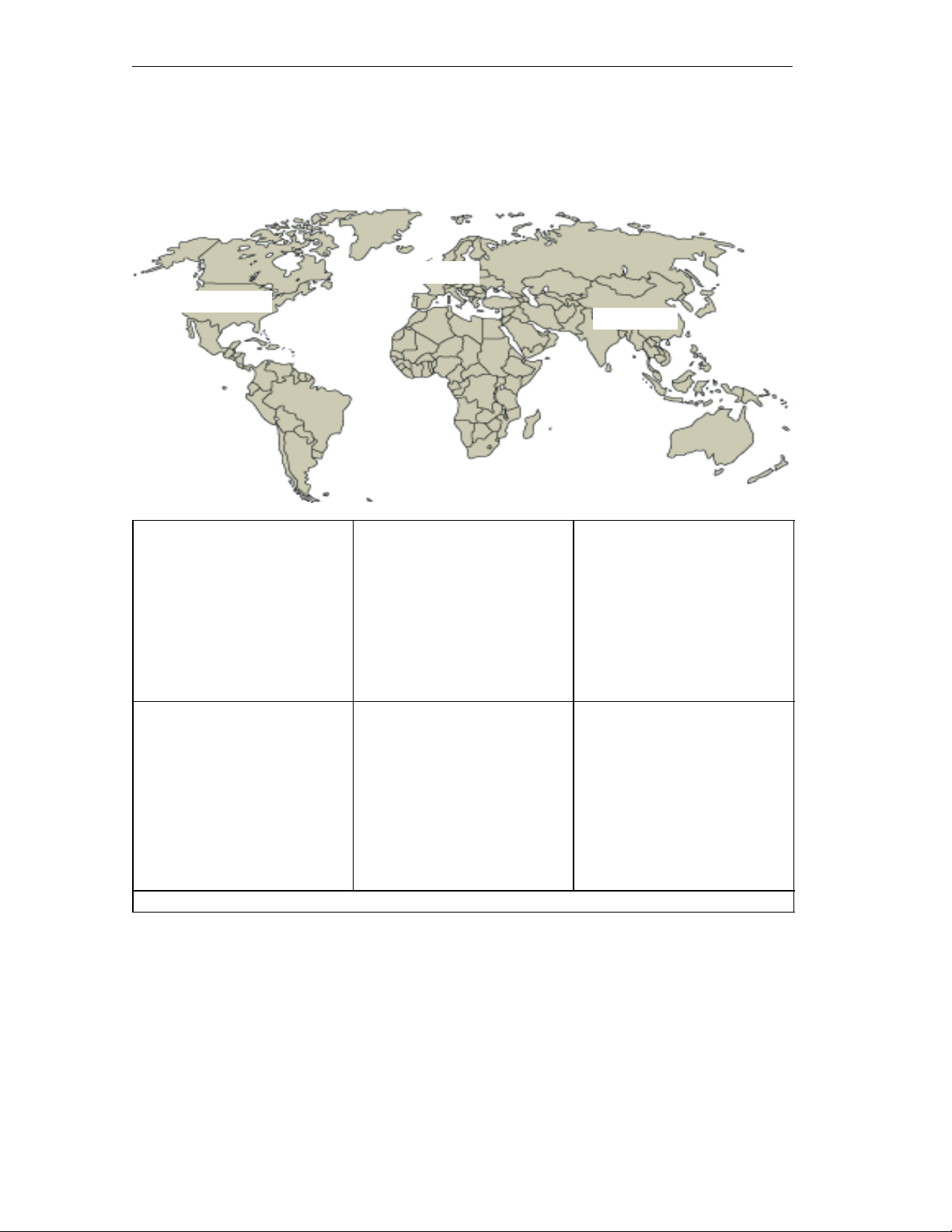
Worldwide, available 24 hours a day:
Johnson City
Nuernberg
Beijing
Technical Support
Worldwide (Nuernberg)
Technical Support
24 hours a day, 365 days a year
Phone: +49 (180) 5050-222
Fax: +49 (180) 5050-223
E-Mail: adsupport@
GMT: +1:00
Europe / Africa (Nuernberg)
Authorization
Local time: Mon.-Fri.
8:00 AM to 5:00 PM
Phone: +49 (180) 5050–222
Fax: +49 (180) 5050-223
E-Mail: adsupport@
GMT: +1:00
The languages of the SIMATIC Hotlines and the authorization hotline are generally German and English.
siemens.com
siemens.com
United States (Johnson City)
Technical Support and
Authorization
Local time: Mon.-Fri.
8:00 AM to 500 PM
Phone: +1 (423) 262 2522
Fax: +1 (423) 262 2289
E-Mail: simatic.hotline@
sea.siemens.com
GMT: –5:00
Asia / Australia (Beijing)
Technical Support and
Authorization
Local time: Mon.-Fri.
8:00 AM to 5:00 PM
Phone: +86 10 64 75 75 75
Fax: +86 10 64 74 74 74
E-Mail: adsupport.asia@
siemens.com
GMT: +8:00
viii
S7-400, M7-400 Programmable Controllers Module Specifications
A5E00069467-07

Service & Support on the Internet
In addition to our documentation, we offer our Know-how online on the internet at:
http://www.siemens.com/automation/service&support
where you will find the following:
• The newsletter, which constantly provides you with up–to–date information on
your products.
• The right documents via our Search function in Service & Support.
• A forum, where users and experts from all over the world exchange their
experiences.
• Your local representative for Automation & Drives via our representatives
database.
• Information on field service, repairs, spare parts and more under “Services”.
Preface
S7-400, M7-400 Programmable Controllers Module Specifications
A5E00069467-07
ix

Preface
x
S7-400, M7-400 Programmable Controllers Module Specifications
A5E00069467-07

Contents
1 General Technical Specifications 1-1. . . . . . . . . . . . . . . . . . . . . . . . . . . . . . . . . . . . . . . . .
1.1 Standards and Approvals 1-2. . . . . . . . . . . . . . . . . . . . . . . . . . . . . . . . . . . . . . . . .
1.2 Electromagnetic Compatibility 1-9. . . . . . . . . . . . . . . . . . . . . . . . . . . . . . . . . . . . .
1.3 Shipping and Storage Conditions for Modules and Backup Batteries 1-12. . . .
1.4 Mechanical and Ambient Climatic Conditions for Operating
the S7-400/M7-400 1-14. . . . . . . . . . . . . . . . . . . . . . . . . . . . . . . . . . . . . . . . . . . . . . .
1.5 Information on Insulation Tests, Protection Class and
Degree of Protection 1-18. . . . . . . . . . . . . . . . . . . . . . . . . . . . . . . . . . . . . . . . . . . . .
1.6 Using S7-400 in a zone 2 explosion–risk area 1-19. . . . . . . . . . . . . . . . . . . . . . .
2 Racks 2-1. . . . . . . . . . . . . . . . . . . . . . . . . . . . . . . . . . . . . . . . . . . . . . . . . . . . . . . . . . . . . . . . . .
2.1 Function and Structure of the Racks 2-2. . . . . . . . . . . . . . . . . . . . . . . . . . . . . . . .
2.2 The Racks UR1; (6ES7400-1TA01-0AA0) and
UR2; (6ES7400-1JA01-0AA0) 2-3. . . . . . . . . . . . . . . . . . . . . . . . . . . . . . . . . . . . .
2.3 The Rack UR2-H; (6ES7400-2JA00-0AA0) 2-5. . . . . . . . . . . . . . . . . . . . . . . . . .
2.4 The Rack CR2; (6ES7401-2TA01-0AA0) 2-7. . . . . . . . . . . . . . . . . . . . . . . . . . . .
2.5 The Rack CR3; (6ES7401-2TA01-0AA0) 2-8. . . . . . . . . . . . . . . . . . . . . . . . . . . .
2.6 The Racks ER1; (6ES7403-1TA01-0AA0)
and ER2; (6ES7403-1JA01-0AA0) 2-9. . . . . . . . . . . . . . . . . . . . . . . . . . . . . . . . .
3 Power Supply Modules 3-1. . . . . . . . . . . . . . . . . . . . . . . . . . . . . . . . . . . . . . . . . . . . . . . . . .
3.1 Common Characteristics of the Power Supply Modules 3-2. . . . . . . . . . . . . . .
3.2 Redundant Power Supply Modules 3-4. . . . . . . . . . . . . . . . . . . . . . . . . . . . . . . . .
3.3 Backup Battery (Option) 3-6. . . . . . . . . . . . . . . . . . . . . . . . . . . . . . . . . . . . . . . . . .
3.4 Controls and Indicators 3-8. . . . . . . . . . . . . . . . . . . . . . . . . . . . . . . . . . . . . . . . . . .
3.5 Fault/Error Messages via LEDs 3-13. . . . . . . . . . . . . . . . . . . . . . . . . . . . . . . . . . . .
3.6 Power Supply Module PS 407 4A; (6ES7407-0DA00-0AA0) 3-19. . . . . . . . . . .
3.7 Power Supply Module PS 407 4A; (6ES7407-0DA01-0AA0) 3-21. . . . . . . . . . .
3.8 Power Supply Modules
PS 407 10A; (6ES7407-0KA01-0AA0) and
PS 407 10A R; (6ES7407-0KR00-0AA0) 3-23. . . . . . . . . . . . . . . . . . . . . . . . . . . .
3.9 Power Supply Module PS 407 20A; (6ES7407-0RA00-0AA0) 3-26. . . . . . . . . .
3.10 Power Supply Module PS 407 20A; (6ES7407-0RA01-0AA0) 3-28. . . . . . . . . .
3.11 Power Supply Module PS 405 4A; (6ES7405-0DA00-0AA0) 3-30. . . . . . . . . . .
S7-400, M7-400 Programmable Controllers Module Specifications
A5E00069467-07
xi

Contents
3.12 Power Supply Module PS 405 4A; (6ES7405-0DA01-0AA0) 3-32. . . . . . . . . . .
3.13 Power Supply Module PS 405 10A; (6ES7405-0KA00-0AA0) 3-34. . . . . . . . . .
3.14 Power Supply Modules
PS 405 10A; (6ES7405-0KA01-0AA0) and
PS 405 10A R; (405-0KR00-0AA0) 3-36. . . . . . . . . . . . . . . . . . . . . . . . . . . . . . . . .
3.15 Power Supply Module PS 405 20A; (6ES7405-0RA00-0AA0) 3-38. . . . . . . . . .
3.16 Power Supply Module PS 405 20A; (6ES7405-0RA01-0AA0) 3-40. . . . . . . . . .
4 Digital Modules 4-1. . . . . . . . . . . . . . . . . . . . . . . . . . . . . . . . . . . . . . . . . . . . . . . . . . . . . . . . .
4.1 Module Overview 4-3. . . . . . . . . . . . . . . . . . . . . . . . . . . . . . . . . . . . . . . . . . . . . . . .
4.2 Sequence of Steps from Choosing to Commissioning the Digital Module 4-5
4.3 Digital Module Parameter Assignment 4-6. . . . . . . . . . . . . . . . . . . . . . . . . . . . . .
4.3.1 Parameters of the Digital Input Modules 4-7. . . . . . . . . . . . . . . . . . . . . . . . . . . . .
4.3.2 Parameters of the Digital Output Modules 4-8. . . . . . . . . . . . . . . . . . . . . . . . . . .
4.4 Diagnostics of the Digital Modules 4-9. . . . . . . . . . . . . . . . . . . . . . . . . . . . . . . . . .
4.5 Interrupts of the Digital Modules 4-13. . . . . . . . . . . . . . . . . . . . . . . . . . . . . . . . . . . .
4.6 Input Characteristic Curve for Digital Inputs 4-15. . . . . . . . . . . . . . . . . . . . . . . . . .
4.7 Digital Input Module SM 421; DI 32 24 VDC
(6ES7421-1BL00-0AA0) 4-17. . . . . . . . . . . . . . . . . . . . . . . . . . . . . . . . . . . . . . . . . .
4.8 Digital Input Module SM 421; DI 32 24 VDC;
(6ES7421-1BL01-0AA0) 4-20. . . . . . . . . . . . . . . . . . . . . . . . . . . . . . . . . . . . . . . . . .
4.9 Digital Input Module SM 421; DI 16 24 VDC;
(6ES7421-7BH00-0AB0) 4-23. . . . . . . . . . . . . . . . . . . . . . . . . . . . . . . . . . . . . . . . . .
4.9.1 Assigning Parameters to the SM 421; DI 16 24 VDC 4-27. . . . . . . . . . . . . . .
4.9.2 Behavior of the SM 421; DI 16 24 VDC 4-29. . . . . . . . . . . . . . . . . . . . . . . . . .
4.10 Digital Input Module SM 421; DI 16 24 VDC;
(6ES7421-7BH00-0AB0) 4-32. . . . . . . . . . . . . . . . . . . . . . . . . . . . . . . . . . . . . . . . . .
4.10.1 Assigning Parameters to the SM 421; DI 16 24 VDC 4-36. . . . . . . . . . . . . . .
4.10.2 Behavior of the SM 421; DI 16 24 VDC 4-38. . . . . . . . . . . . . . . . . . . . . . . . . . . .
4.11 Digital Input Module SM 421; DI 16 120 VAC;
(6ES7421-5EH00-0AA0) 4-41. . . . . . . . . . . . . . . . . . . . . . . . . . . . . . . . . . . . . . . . . .
4.12 Digital Input Module SM 421; DI 16 24/60 VUC;
(6ES7 421-7DH00-0AB0) 4-44. . . . . . . . . . . . . . . . . . . . . . . . . . . . . . . . . . . . . . . . .
4.12.1 Assigning Parameters to the SM 421; DI 16 24/60 VUC 4-47. . . . . . . . . . . .
4.13 Digital Input Module SM 421; DI 16 120/230 VUC;
(6ES7 421-1FH00-0AA0) 4-50. . . . . . . . . . . . . . . . . . . . . . . . . . . . . . . . . . . . . . . . .
4.14 Digital Input Module SM 421; DI 16 120/230 VUC;
(6ES7421-1FH20-0AA0) 4-53. . . . . . . . . . . . . . . . . . . . . . . . . . . . . . . . . . . . . . . . . .
4.15 Digital Input Module SM 421; DI 32 120 VUC;
(6ES7421-1EL00-0AA0) 4-56. . . . . . . . . . . . . . . . . . . . . . . . . . . . . . . . . . . . . . . . . .
4.16 Digital Output Module SM 422;
DO 16 24 VDC/2 A; (6ES7422-1BH10-0AA0) 4-59. . . . . . . . . . . . . . . . . . . . .
S7-400, M7-400 Programmable Controllers Module Specifications
xii
A5E00069467-07

Contents
4.17 Digital Output Module SM 422;
DO 16 24 VDC/2 A; (6ES7422-1BH11-0AA0) 4-62. . . . . . . . . . . . . . . . . . . . .
4.18 Digital Output Module SM 422; DO 16 0-125 VDC/1.5 A;
(6ES7422-5EH10-0AB0) 4-65. . . . . . . . . . . . . . . . . . . . . . . . . . . . . . . . . . . . . . . . . .
4.18.1 Assigning Parameters to the SM 422; DO 16 20-125 VDC/1.5 A 4-69. . . .
4.19 Digital Output Module SM 422; DO 32 24 VDC/0.5 A;
(6ES7422-1BL00-0AA0) 4-70. . . . . . . . . . . . . . . . . . . . . . . . . . . . . . . . . . . . . . . . . .
4.20 Digital Output Module SM 422; DO 32 24 VDC/0.5 A;
(6ES7422-7BL00-0AB0) 4-73. . . . . . . . . . . . . . . . . . . . . . . . . . . . . . . . . . . . . . . . . .
4.20.1 Assigning Parameters to the SM 422; DO 32 24 VDC/0.5 A 4-77. . . . . . . .
4.20.2 Behavior of the SM 422; DO 32 24 VDC/0.5 A 4-78. . . . . . . . . . . . . . . . . . . .
4.21 Digital Output Module SM 422; DO 8 120/230 VAC/5 A;
(6ES7422-1FF00-0AA0) 4-79. . . . . . . . . . . . . . . . . . . . . . . . . . . . . . . . . . . . . . . . . .
4.22 Digital Output Module SM 422; DO 16 120/230 VAC/2 A;
(6ES7422-1FH00-0AA0) 4-83. . . . . . . . . . . . . . . . . . . . . . . . . . . . . . . . . . . . . . . . . .
4.23 Digital Output Module SM 422; DO 16 20-120 VAC/2 A;
(6ES7422-5EH00-0AB0) 4-87. . . . . . . . . . . . . . . . . . . . . . . . . . . . . . . . . . . . . . . . . .
4.23.1 Assigning Parameters to the SM 422; DO 16 20-120 VAC/2 A 4-90. . . . . .
4.24 Relay Output Module SM 422; DO 16 30/230 VUC/Rel. 5 A;
(6ES7422-1HH00-0AA0) 4-91. . . . . . . . . . . . . . . . . . . . . . . . . . . . . . . . . . . . . . . . . .
5 Analog Modules 5-1. . . . . . . . . . . . . . . . . . . . . . . . . . . . . . . . . . . . . . . . . . . . . . . . . . . . . . . . .
5.1 Module Overview 5-3. . . . . . . . . . . . . . . . . . . . . . . . . . . . . . . . . . . . . . . . . . . . . . . .
5.2 Sequence of Steps from Choosing to Commissioning
the Analog Modules 5-5. . . . . . . . . . . . . . . . . . . . . . . . . . . . . . . . . . . . . . . . . . . . . .
5.3 Analog Value Representation 5-6. . . . . . . . . . . . . . . . . . . . . . . . . . . . . . . . . . . . . .
5.3.1 Analog Value Representation for Analog Input Channels 5-7. . . . . . . . . . . . . .
5.3.2 Analog Value Representation for Analog Output Channels 5-22. . . . . . . . . . . . .
5.4 Setting the Measuring Method and Measuring Ranges
of the Analog Input Channels 5-27. . . . . . . . . . . . . . . . . . . . . . . . . . . . . . . . . . . . . .
5.5 Behavior of the Analog Modules 5-30. . . . . . . . . . . . . . . . . . . . . . . . . . . . . . . . . . .
5.5.1 Effect of Supply Voltage and Operating Mode 5-30. . . . . . . . . . . . . . . . . . . . . . . .
5.5.2 Effect of Range of Values of the Analog Values 5-31. . . . . . . . . . . . . . . . . . . . . .
5.5.3 Effect of Operational Limit and Basic Error Limit 5-32. . . . . . . . . . . . . . . . . . . . . .
5.6 Conversion, Cycle, Setting and Response Time of Analog Modules 5-34. . . . .
5.7 Analog Module Parameter Assignment 5-38. . . . . . . . . . . . . . . . . . . . . . . . . . . . . .
5.7.1 Parameters of the Analog Input Modules 5-39. . . . . . . . . . . . . . . . . . . . . . . . . . . .
5.7.2 Parameters of the Analog Output Modules 5-41. . . . . . . . . . . . . . . . . . . . . . . . . .
5.8 Connecting Sensors to Analog Inputs 5-42. . . . . . . . . . . . . . . . . . . . . . . . . . . . . . .
5.9 Connecting Voltage Sensors 5-45. . . . . . . . . . . . . . . . . . . . . . . . . . . . . . . . . . . . . . .
5.10 Connecting Current Sensors 5-46. . . . . . . . . . . . . . . . . . . . . . . . . . . . . . . . . . . . . . .
5.11 Connecting Resistance Thermometers and Resistors 5-49. . . . . . . . . . . . . . . . .
5.12 Connecting Thermocouples 5-52. . . . . . . . . . . . . . . . . . . . . . . . . . . . . . . . . . . . . . .
S7-400, M7-400 Programmable Controllers Module Specifications
A5E00069467-07
xiii

Contents
5.13 Connecting Loads/Actuators to Analog Outputs 5-58. . . . . . . . . . . . . . . . . . . . . .
5.14 Connecting Loads/Actuators to Voltage Outputs 5-59. . . . . . . . . . . . . . . . . . . . . .
5.15 Connecting Loads/Actuators to Current Outputs 5-61. . . . . . . . . . . . . . . . . . . . . .
5.16 Diagnostics of the Analog Modules 5-62. . . . . . . . . . . . . . . . . . . . . . . . . . . . . . . . .
5.17 Analog Module Interrupts 5-66. . . . . . . . . . . . . . . . . . . . . . . . . . . . . . . . . . . . . . . . .
5.18 Analog Input Module SM 431; AI 8 13 Bit; (6ES7431-1KF00-0AB0) 5-69. .
5.18.1 Commissioning the SM 431; AI 8 13 Bit 5-73. . . . . . . . . . . . . . . . . . . . . . . . . .
5.18.2 Measuring Methods and Measuring Ranges of the SM 431; AI 8 13 Bit 5-74.
5.19 Analog Input Module SM 431; AI 8 14 Bit; (6ES7 431-1KF10-0AB0) 5-76.
5.19.1 Commissioning the SM 431; AI 8 14 Bit 5-82. . . . . . . . . . . . . . . . . . . . . . . . . .
5.19.2 Measuring Methods and Measuring Ranges of the SM 431; AI 8 14 Bit 5-84.
5.20 Analog Input Module SM 431; AI 8 4 Bit; (6ES7431-1KF20-0AB0) 5-89. . .
5.20.1 Commissioning the SM 431; AI 8 14 Bit 5-93. . . . . . . . . . . . . . . . . . . . . . . . . .
5.20.2 Measuring Methods and Measuring Ranges
of the SM 431; AI 8 14 Bit 5-95. . . . . . . . . . . . . . . . . . . . . . . . . . . . . . . . . . . . . .
5.21 Analog Input Module SM 431; AI 16 13 Bit; (6ES7431-0HH00-0AB0) 5-98
5.21.1 Commissioning the SM 431; AI 16 13 Bit 5-103. . . . . . . . . . . . . . . . . . . . . . . . .
5.21.2 Measuring Methods and Measuring Ranges
of the SM 431; AI 16 13 Bit 5-104. . . . . . . . . . . . . . . . . . . . . . . . . . . . . . . . . . . . .
5.22 Analog Input Module SM 431; AI 16 16 Bit; (6ES7431-7QH00-0AB0) 5-106
5.22.1 Commissioning the SM 431; AI 16 16 Bit 5-114. . . . . . . . . . . . . . . . . . . . . . . . .
5.22.2 Measuring Methods and Measuring Ranges
of the SM 431; AI 16 16 Bit 5-117. . . . . . . . . . . . . . . . . . . . . . . . . . . . . . . . . . . . .
5.23 Analog Input Module SM 431; AI 8 RTD 16 Bit;
(6ES7 431-7KF10-0AB0) 5-122. . . . . . . . . . . . . . . . . . . . . . . . . . . . . . . . . . . . . . . . . .
5.23.1 Commissioning the SM 431; AI 8 RTD 16 Bit 5-126. . . . . . . . . . . . . . . . . .
5.23.2 Measuring Methods and Measuring Ranges
of the SM 431; AI 8 RTD 16 Bit 5-129. . . . . . . . . . . . . . . . . . . . . . . . . . . . . .
5.24 Analog Input Module SM 431; AI 8 16 Bit;
(6ES7431-7KF00-0AB0) 5-130. . . . . . . . . . . . . . . . . . . . . . . . . . . . . . . . . . . . . . . . . .
5.24.1 Commissioning the SM 431; AI 8 16 Bit 5-135. . . . . . . . . . . . . . . . . . . . . . . . . .
5.24.2 Measuring Methods and Measuring Ranges of the SM 431;
AI 8 16 Bit 5-139. . . . . . . . . . . . . . . . . . . . . . . . . . . . . . . . . . . . . . . . . . . . . . . . . . .
5.25 Analog Output Module SM 432; AO 8 13 Bit;
(6ES7432-1HF00-0AB0) 5-141. . . . . . . . . . . . . . . . . . . . . . . . . . . . . . . . . . . . . . . . . .
5.25.1 Commissioning the SM 432; AO 8 13 Bit 5-145. . . . . . . . . . . . . . . . . . . . . . . . .
5.25.2 Output Ranges of the Analog Output Module SM 432;
AO 8 13 Bit 5-145. . . . . . . . . . . . . . . . . . . . . . . . . . . . . . . . . . . . . . . . . . . . . . . . . .
xiv
S7-400, M7-400 Programmable Controllers Module Specifications
A5E00069467-07

Contents
6 Interface Modules 6-1. . . . . . . . . . . . . . . . . . . . . . . . . . . . . . . . . . . . . . . . . . . . . . . . . . . . . . .
6.1 Common Features of the Interface Modules 6-2. . . . . . . . . . . . . . . . . . . . . . . . .
6.2 The Interface Modules
IM 460-0; (6ES7460-0AA00-0AB0, 6ES7460-0AA01-0AB0)
and IM 461-0; (6ES7461-0AA00-0AA0, 6ES7461-0AA01-0AA0) 6-7. . . . . . .
6.3 The Interface Modules
IM 460-1; (6ES7460-1BA00-0AB0, 6ES7460-1BA01-0AB0)
and IM 461-1; (6ES7461-1BA00-0AA0, 6ES7461-1BA01-0AA0) 6-10. . . . . . .
6.4 The Interface Modules
IM 460-3; (6ES7460-3AA00-0AB0, 6ES7460-3AA01-0AB0)
and IM 461-3; (6ES7461-3AA00-0AA0, 6ES7461-3AA01-0AA0) 6-14. . . . . . .
6.5 The Interface Modules
IM 460-4; (6ES7460-4AA01-0AB0) and
IM 461-4; (6ES7461-4AA01-0AA0) 6-18. . . . . . . . . . . . . . . . . . . . . . . . . . . . . . . . .
7 IM 463-2 7-1. . . . . . . . . . . . . . . . . . . . . . . . . . . . . . . . . . . . . . . . . . . . . . . . . . . . . . . . . . . . . . . .
7.1 Using SIMATIC S5 Expansion Units in an S7-400 7-2. . . . . . . . . . . . . . . . . . . .
7.2 Rules for Connecting S5 Expansion Units 7-3. . . . . . . . . . . . . . . . . . . . . . . . . . .
7.3 Operator Controls and Indicators 7-4. . . . . . . . . . . . . . . . . . . . . . . . . . . . . . . . . . .
7.4 Installing and Connecting the IM 463-2 7-6. . . . . . . . . . . . . . . . . . . . . . . . . . . . .
7.5 Setting the Operating Modes of the IM 314 7-8. . . . . . . . . . . . . . . . . . . . . . . . . .
7.6 Configuring S5 Modules for Operation in the S7-400 7-10. . . . . . . . . . . . . . . . . .
7.7 Pin Assignments of the 721 Connecting Cable 7-11. . . . . . . . . . . . . . . . . . . . . . .
7.8 Terminating Connector for IM 314 7-13. . . . . . . . . . . . . . . . . . . . . . . . . . . . . . . . . .
7.9 Technical Specifications (6ES7463–2AA00–0AA0) 7-14. . . . . . . . . . . . . . . . . . .
8 PROFIBUS DP Master Interface IM 467/IM 467 FO 8-1. . . . . . . . . . . . . . . . . . . . . . . . . .
8.1 PROFIBUS DP Master Interface IM 467/IM 467 FO 8-2. . . . . . . . . . . . . . . . . .
8.1.1 Indicators and the Mode Selector 8-4. . . . . . . . . . . . . . . . . . . . . . . . . . . . . . . . . .
8.2 Configuration 8-6. . . . . . . . . . . . . . . . . . . . . . . . . . . . . . . . . . . . . . . . . . . . . . . . . . . .
8.3 Connection to PROFIBUS DP 8-8. . . . . . . . . . . . . . . . . . . . . . . . . . . . . . . . . . . . .
8.3.1 Bus Connector 8-8. . . . . . . . . . . . . . . . . . . . . . . . . . . . . . . . . . . . . . . . . . . . . . . . . . .
8.3.2 Optical Connection to PROFIBUS DP 8-9. . . . . . . . . . . . . . . . . . . . . . . . . . . . . . .
8.3.3 Connecting a Fiber-Optic Cable to the IM 467 FO 8-10. . . . . . . . . . . . . . . . . . . .
8.4 Technical Specifications 8-12. . . . . . . . . . . . . . . . . . . . . . . . . . . . . . . . . . . . . . . . . . .
8.4.1 Technical Specifications of the IM 467 8-12. . . . . . . . . . . . . . . . . . . . . . . . . . . . . .
8.4.2 Technical Specifications of the IM 467 FO 8-13. . . . . . . . . . . . . . . . . . . . . . . . . . .
9 Cable Duct and Fan Subassemblies 9-1. . . . . . . . . . . . . . . . . . . . . . . . . . . . . . . . . . . . . .
9.1 Fan Monitoring in the Fan Subassemblies 9-2. . . . . . . . . . . . . . . . . . . . . . . . . . .
9.2 Cable Duct; (6ES7408-0TA00-0AA0) 9-4. . . . . . . . . . . . . . . . . . . . . . . . . . . . . . .
9.3 The 120/230 VAC Fan Subassembly; (6ES7408-1TB00-0XA0) 9-5. . . . . . . . .
9.4 The 24 VDC Fan Subassembly; (6ES7408-1TA00-0XA0) 9-7. . . . . . . . . . . . . .
S7-400, M7-400 Programmable Controllers Module Specifications
A5E00069467-07
xv

Contents
10 RS 485 Repeater 10-1. . . . . . . . . . . . . . . . . . . . . . . . . . . . . . . . . . . . . . . . . . . . . . . . . . . . . . . . .
10.1 Application and Characteristics (6ES7972-0AA01-0XA0) 10-2. . . . . . . . . . . . . .
10.2 Appearance of the RS 485 Repeater; (6ES7972-0AA01-0XA0) 10-3. . . . . . . .
10.3 RS 485 Repeater in Ungrounded and Grounded Operation 10-4. . . . . . . . . . . .
10.4 Technical Specifications 10-6. . . . . . . . . . . . . . . . . . . . . . . . . . . . . . . . . . . . . . . . . . .
11 CPUs for M7-400 11-1. . . . . . . . . . . . . . . . . . . . . . . . . . . . . . . . . . . . . . . . . . . . . . . . . . . . . . . .
11.1 Performance Features 11-2. . . . . . . . . . . . . . . . . . . . . . . . . . . . . . . . . . . . . . . . .
11.2 Technical Specifications 11-3. . . . . . . . . . . . . . . . . . . . . . . . . . . . . . . . . . . . . . . . . . .
11.3 Function Elements 11-4. . . . . . . . . . . . . . . . . . . . . . . . . . . . . . . . . . . . . . . . . . . . . . .
11.3.1 Status and Fault LEDs 11-6. . . . . . . . . . . . . . . . . . . . . . . . . . . . . . . . . . . . . . . . . . . .
11.3.2 Memory Cards 11-8. . . . . . . . . . . . . . . . . . . . . . . . . . . . . . . . . . . . . . . . . . . . . . . . . . .
11.3.3 Mode Selector Switch 11-9. . . . . . . . . . . . . . . . . . . . . . . . . . . . . . . . . . . . . . . . . . . .
11.3.4 Submodule Receptacles for Interface Submodules 11-11. . . . . . . . . . . . . . . . . . .
11.3.5 Memory Submodules Suitable for the Main Memory 11-13. . . . . . . . . . . . . . . . . .
11.3.6 Expansion Socket 11-14. . . . . . . . . . . . . . . . . . . . . . . . . . . . . . . . . . . . . . . . . . . . . . . .
11.3.7 Multipoint Interface (MPI) 11-15. . . . . . . . . . . . . . . . . . . . . . . . . . . . . . . . . . . . . . . . .
11.4 The BIOS Setup 11-16. . . . . . . . . . . . . . . . . . . . . . . . . . . . . . . . . . . . . . . . . . . . . . . . .
11.4.1 BIOS Power Up 11-17. . . . . . . . . . . . . . . . . . . . . . . . . . . . . . . . . . . . . . . . . . . . . . . . . .
11.4.2 BIOS Hot Keys 11-19. . . . . . . . . . . . . . . . . . . . . . . . . . . . . . . . . . . . . . . . . . . . . . . . . .
11.4.3 Operator Inputs in the BIOS Setup 11-20. . . . . . . . . . . . . . . . . . . . . . . . . . . . . . . . .
11.4.4 Opening and Exiting the BIOS Setup 11-23. . . . . . . . . . . . . . . . . . . . . . . . . . . . . . .
11.4.5 Setup Page “User Help” 11-25. . . . . . . . . . . . . . . . . . . . . . . . . . . . . . . . . . . . . . . . . . .
11.4.6 Setup Page “IF modules” 11-26. . . . . . . . . . . . . . . . . . . . . . . . . . . . . . . . . . . . . . . . . .
11.4.7 Setup Page “Timeout Function” 11-30. . . . . . . . . . . . . . . . . . . . . . . . . . . . . . . . . . . .
11.4.8 Setup Page “Security” 11-31. . . . . . . . . . . . . . . . . . . . . . . . . . . . . . . . . . . . . . . . . . . .
11.4.9 Setup Page “Date and Time” 11-33. . . . . . . . . . . . . . . . . . . . . . . . . . . . . . . . . . . . . .
11.4.10 “Hard Disk” Setup Page 11-34. . . . . . . . . . . . . . . . . . . . . . . . . . . . . . . . . . . . . . . . . . .
11.4.11 Setup Page “Floppy/Card” 11-36. . . . . . . . . . . . . . . . . . . . . . . . . . . . . . . . . . . . . . . . .
11.4.12 Setup Page “Boot Options” 11-37. . . . . . . . . . . . . . . . . . . . . . . . . . . . . . . . . . . . . . . .
11.4.13 Setup Page “System” 11-39. . . . . . . . . . . . . . . . . . . . . . . . . . . . . . . . . . . . . . . . . . . . .
11.5 I/O Addresses, Main Memory and Interrupt Assignments 11-41. . . . . . . . . . . . . .
12 M7-400 Expansions 12-1. . . . . . . . . . . . . . . . . . . . . . . . . . . . . . . . . . . . . . . . . . . . . . . . . . . . . .
12.1 Overview 12-2. . . . . . . . . . . . . . . . . . . . . . . . . . . . . . . . . . . . . . . . . . . . . . . . . . . . . . .
12.2 EXM 478 Expansion Module; (6ES7 478-2AC00-0AC0) 12-6. . . . . . . . . . . . . . .
12.2.1 Addressing the EXM 478 Expansion Module 12-7. . . . . . . . . . . . . . . . . . . . . . . . .
12.2.2 Interrupt Assignments, Signal Switching EXM 478 12-13. . . . . . . . . . . . . . . . . . . .
12.2.3 Technical Specifications of the EXM 478 Expansion Module 12-14. . . . . . . . . . .
12.3 ATM 478 AT Adapter Module; (6ES7 478-2CA00-0AC0) 12-15. . . . . . . . . . . . . .
12.3.1 Pin Assignments of the AT Module 12-16. . . . . . . . . . . . . . . . . . . . . . . . . . . . . . . . .
12.3.2 Technical Specifications of the ATM 478 AT Adapter Module 12-19. . . . . . . . . . .
12.4 MSM 478 Mass Storage Module; (6ES7 478-2BA00-0AC0) 12-22. . . . . . . . . . . .
12.4.1 LPT1 Parallel Port 12-23. . . . . . . . . . . . . . . . . . . . . . . . . . . . . . . . . . . . . . . . . . . . . . . .
12.4.2 Technical Specifications of the MSM 478 Mass Storage Module 12-25. . . . . . . .
S7-400, M7-400 Programmable Controllers Module Specifications
xvi
A5E00069467-07

Contents
13 Interface Submodules 13-1. . . . . . . . . . . . . . . . . . . . . . . . . . . . . . . . . . . . . . . . . . . . . . . . . . .
13.1 Interface Submodules Overview 13-2. . . . . . . . . . . . . . . . . . . . . . . . . . . . . . . . . . .
13.2 Submodule IDs and Insertion Rules 13-4. . . . . . . . . . . . . . . . . . . . . . . . . . . . . . . .
13.3 IF 962-VGA Interface Submodule for M7-300/400;
(6ES7962-1BA00-0AC0) 13-5. . . . . . . . . . . . . . . . . . . . . . . . . . . . . . . . . . . . . . . . . .
13.3.1 Pin Assignments 13-6. . . . . . . . . . . . . . . . . . . . . . . . . . . . . . . . . . . . . . . . . . . . . . . . .
13.3.2 Addressing, Interrupts, and Submodule ID 13-7. . . . . . . . . . . . . . . . . . . . . . . . . .
13.3.3 Technical Specifications 13-8. . . . . . . . . . . . . . . . . . . . . . . . . . . . . . . . . . . . . . . . . . .
13.4 IF 962-COM Interface Submodule for M7-300/400;
(6ES7962-3AA00-0AC0) 13-10. . . . . . . . . . . . . . . . . . . . . . . . . . . . . . . . . . . . . . . . . .
13.4.1 Pin Assignments 13-11. . . . . . . . . . . . . . . . . . . . . . . . . . . . . . . . . . . . . . . . . . . . . . . . .
13.4.2 Addressing and Interrupts 13-12. . . . . . . . . . . . . . . . . . . . . . . . . . . . . . . . . . . . . . . . .
13.4.3 Technical Specifications 13-15. . . . . . . . . . . . . . . . . . . . . . . . . . . . . . . . . . . . . . . . . . .
13.5 IF 962-LPT Interface Submodule for M7-300/400;
(6ES7962-4AA00-0AC0) 13-16. . . . . . . . . . . . . . . . . . . . . . . . . . . . . . . . . . . . . . . . . .
13.5.1 Pin Assignments 13-17. . . . . . . . . . . . . . . . . . . . . . . . . . . . . . . . . . . . . . . . . . . . . . . . .
13.5.2 Addressing and Interrupts 13-18. . . . . . . . . . . . . . . . . . . . . . . . . . . . . . . . . . . . . . . . .
13.5.3 Technical Specifications 13-22. . . . . . . . . . . . . . . . . . . . . . . . . . . . . . . . . . . . . . . . . . .
13.6 IF 961-DIO Interface Submodule for M7-300/400;
(6ES7961-1AA00-0AC0) 13-23. . . . . . . . . . . . . . . . . . . . . . . . . . . . . . . . . . . . . . . . . .
13.6.1 Pin Assignments 13-24. . . . . . . . . . . . . . . . . . . . . . . . . . . . . . . . . . . . . . . . . . . . . . . . .
13.6.2 Addressing and Interrupts 13-26. . . . . . . . . . . . . . . . . . . . . . . . . . . . . . . . . . . . . . . . .
13.6.3 Technical Specifications 13-31. . . . . . . . . . . . . . . . . . . . . . . . . . . . . . . . . . . . . . . . . . .
13.7 IF 961-AIO Interface Submodule for M7-300/400;
(6ES7961-2AA00-0AC0) 13-33. . . . . . . . . . . . . . . . . . . . . . . . . . . . . . . . . . . . . . . . . .
13.7.1 Pin Assignments and Terminal Connection Diagram 13-34. . . . . . . . . . . . . . . . . .
13.7.2 Connecting Measured Value Sensors to Analog Inputs 13-37. . . . . . . . . . . . . . . .
13.7.3 Connecting Loads/Actuators to Analog Outputs 13-42. . . . . . . . . . . . . . . . . . . . . .
13.7.4 Conversion Time and Cycle Time of the Analog Input Channels 13-44. . . . . . . .
13.7.5 Conversion Time, Cycle Time, Settling Time,
and Response Time of the Analog Output Channels 13-45. . . . . . . . . . . . . . . . . .
13.7.6 Starting Up the IF 961-AIO Interface Submodule 13-46. . . . . . . . . . . . . . . . . . . . .
13.7.7 Addressing 13-46. . . . . . . . . . . . . . . . . . . . . . . . . . . . . . . . . . . . . . . . . . . . . . . . . . . . . .
13.7.8 Analog Output Function 13-47. . . . . . . . . . . . . . . . . . . . . . . . . . . . . . . . . . . . . . . . . . .
13.7.9 Analog Input Function 13-48. . . . . . . . . . . . . . . . . . . . . . . . . . . . . . . . . . . . . . . . . . . .
13.7.10 Analog Value Representation for the Measuring Ranges
of the Analog Inputs 13-51. . . . . . . . . . . . . . . . . . . . . . . . . . . . . . . . . . . . . . . . . . . . . .
13.7.11 Analog Value Representation for the Measuring Ranges
of the Analog Outputs 13-52. . . . . . . . . . . . . . . . . . . . . . . . . . . . . . . . . . . . . . . . . . . .
13.7.12 Diagnostics, Interrupts, and Submodule ID 13-53. . . . . . . . . . . . . . . . . . . . . . . . . .
13.7.13 Technical Specifications 13-54. . . . . . . . . . . . . . . . . . . . . . . . . . . . . . . . . . . . . . . . . . .
13.8 IF 961-CT1 Interface Submodule for M7-300/400;
(6ES7961-3AA00-0AC0) 13-56. . . . . . . . . . . . . . . . . . . . . . . . . . . . . . . . . . . . . . . . . .
13.8.1 What Can the IF961-CT1 Interface Submodule Do? 13-57. . . . . . . . . . . . . . . . . .
13.8.2 Addressing and Interrupts 13-59. . . . . . . . . . . . . . . . . . . . . . . . . . . . . . . . . . . . . . . . .
13.8.3 Technical Specifications 13-60. . . . . . . . . . . . . . . . . . . . . . . . . . . . . . . . . . . . . . . . . . .
S7-400, M7-400 Programmable Controllers Module Specifications
A5E00069467-07
xvii

Contents
13.9 IF 964-DP Interface Submodule for S7-400 and M7-400 13-61. . . . . . . . . . . . . .
13.9.1 Pin Assignments 13-63. . . . . . . . . . . . . . . . . . . . . . . . . . . . . . . . . . . . . . . . . . . . . . . . .
13.9.2 Addressing and Interrupts 13-64. . . . . . . . . . . . . . . . . . . . . . . . . . . . . . . . . . . . . . . . .
13.9.3 Technical Specifications 13-65. . . . . . . . . . . . . . . . . . . . . . . . . . . . . . . . . . . . . . . . . . .
A Parameter Sets for Signal Modules A-1. . . . . . . . . . . . . . . . . . . . . . . . . . . . . . . . . . . . . . .
A.1 How to Assign the Parameters for Signal Modules in the User Program A-2.
A.2 Parameters of the Digital Input Modules A-4. . . . . . . . . . . . . . . . . . . . . . . . . . . . .
A.3 Parameters of the Digital Output Modules A-7. . . . . . . . . . . . . . . . . . . . . . . . . . .
A.4 Parameters of the Analog Input Modules A-10. . . . . . . . . . . . . . . . . . . . . . . . . . . .
B Diagnostic Data of the Signal Modules B-1. . . . . . . . . . . . . . . . . . . . . . . . . . . . . . . . . . . .
B.1 Evaluating the Diagnostic Data of the Signal Modules
in the User Program B-2. . . . . . . . . . . . . . . . . . . . . . . . . . . . . . . . . . . . . . . . . . . . . .
B.2 Structure and Contents of
Diagnostic Data Bytes 0 and 1 B-3. . . . . . . . . . . . . . . . . . . . . . . . . . . . . . . . . . . . .
B.3 Diagnostic Data of the Digital Input Modules
as of Byte 2 B-4. . . . . . . . . . . . . . . . . . . . . . . . . . . . . . . . . . . . . . . . . . . . . . . . . . . . .
B.4 Diagnostic Data of the Digital Output Modules
as of Byte 2 B-8. . . . . . . . . . . . . . . . . . . . . . . . . . . . . . . . . . . . . . . . . . . . . . . . . . . . .
B.5 Diagnostic Data of the Analog Input Modules
as of Byte 2 B-14. . . . . . . . . . . . . . . . . . . . . . . . . . . . . . . . . . . . . . . . . . . . . . . . . . . . .
C Spare Parts and Accessories C-1. . . . . . . . . . . . . . . . . . . . . . . . . . . . . . . . . . . . . . . . . . . . .
D Guidelines for Handling Electrostatic Sensitive Devices (ESD) D-1. . . . . . . . . . . . . .
D.1 What is ESD? D-2. . . . . . . . . . . . . . . . . . . . . . . . . . . . . . . . . . . . . . . . . . . . . . . . . . .
D.2 Electrostatic Charging of Persons D-3. . . . . . . . . . . . . . . . . . . . . . . . . . . . . . . . . .
D.3 General Protective Measures Against Electrostatic Discharge Damage D-4.
E List of Abbreviations E-1. . . . . . . . . . . . . . . . . . . . . . . . . . . . . . . . . . . . . . . . . . . . . . . . . . . .
Glossary Glossary-1. . . . . . . . . . . . . . . . . . . . . . . . . . . . . . . . . . . . . . . . . . . . . . . . . . . . .
Index Index-1. . . . . . . . . . . . . . . . . . . . . . . . . . . . . . . . . . . . . . . . . . . . . . . . . . . . . . . .
xviii
S7-400, M7-400 Programmable Controllers Module Specifications
A5E00069467-07

Figures
1-1 Power supply to the backup battery 1-6. . . . . . . . . . . . . . . . . . . . . . . . . . . . . . . . .
2-1 Structure of a Rack with 18 Slots 2-2. . . . . . . . . . . . . . . . . . . . . . . . . . . . . . . . . . .
2-2 Dimensions of the UR1 18-Slot or UR2 9-Slot Rack 2-3. . . . . . . . . . . . . . . . . .
2-3 Rack Dimensions 2-5. . . . . . . . . . . . . . . . . . . . . . . . . . . . . . . . . . . . . . . . . . . . . . . .
2-4 CR2 Rack 2-7. . . . . . . . . . . . . . . . . . . . . . . . . . . . . . . . . . . . . . . . . . . . . . . . . . . . . . .
2-5 CR3 Rack 2-8. . . . . . . . . . . . . . . . . . . . . . . . . . . . . . . . . . . . . . . . . . . . . . . . . . . . . . .
2-6 ER1 Rack with 18 Slots and ER2 Rack with 9 Slots 2-10. . . . . . . . . . . . . . . . . . .
3-1 Controls and Indicators on the PS 407 20A Power Supply Module 3-8. . . . . .
3-2 Controls and Indicators of the PS 407 4A 3-19. . . . . . . . . . . . . . . . . . . . . . . . . . .
3-3 Controls and Indicators of the PS 407 4 A 3-21. . . . . . . . . . . . . . . . . . . . . . . . . . .
3-4 Controls and Displays of the PS 407 10A and PS 407 10A R 3-23. . . . . . . . . .
3-5 Controls and Displays of the PS 407 20A 3-25. . . . . . . . . . . . . . . . . . . . . . . . . . . .
3-6 Controls and Indicators of the PS 407 20 A 3-27. . . . . . . . . . . . . . . . . . . . . . . . . .
3-7 Controls and Indicators of the PS 405 4 A 3-29. . . . . . . . . . . . . . . . . . . . . . . . . . .
3-8 Controls and Indicators of the PS 405 4 A 3-31. . . . . . . . . . . . . . . . . . . . . . . . . . .
3-9 Controls and Indicators of the PS 405 10 A 3-33. . . . . . . . . . . . . . . . . . . . . . . . . .
3-10 Controls and Displays of the PS 405 10A and PS 405 10A R 3-35. . . . . . . . . .
3-11 Controls and Indicators of the PS 405 20 A 3-37. . . . . . . . . . . . . . . . . . . . . . . . . .
3-12 Controls and Indicators of the PS 405 20 A 3-39. . . . . . . . . . . . . . . . . . . . . . . . . .
4-1 Input Characteristic Curve for Digital Inputs 4-16. . . . . . . . . . . . . . . . . . . . . . . . . .
4-2 Terminal Assignment and Block Diagram of the SM 421; DI 32 x 24 VDC 4-18
4-3 Terminal Assignment and Block Diagram of the SM 421; DI 32 x 24 VDC 4-21
4-4 Terminal Assignment and Block Diagram of the SM 421; DI 16 x 24 VDC 4-24
4-5 Terminal Assignment Diagram for the Redundant Supply
of Sensors of the
SM 421; DI 16 x 24 VDC 4-25. . . . . . . . . . . . . . . . . . . . . . . . . . . . . . . . . . . . . . . . . .
4-6 Terminal Assignment and Block Diagram of the SM 421;
DI 16 x 24 VDC 4-33. . . . . . . . . . . . . . . . . . . . . . . . . . . . . . . . . . . . . . . . . . . . . . . . . .
4-7 Terminal Assignment Diagram for the Redundant Supply
of Sensors of the
SM 421; DI 16 x 24 VDC 4-34. . . . . . . . . . . . . . . . . . . . . . . . . . . . . . . . . . . . . . . . . .
4-8 Terminal Assignment Diagram of the SM 421; DI 16 120 VDC 4-42. . . . . . . .
4-9 Terminal Assignment and Block Diagram of the SM 421;
DI 16 x 24/60 VUC 4-45. . . . . . . . . . . . . . . . . . . . . . . . . . . . . . . . . . . . . . . . . . . . . . .
4-10 Circuit as for Active High or Active Low Input 4-49. . . . . . . . . . . . . . . . . . . . . . . .
4-11 Terminal Assignment and Block Diagram of the SM 421;
DI 16 x 120/230 VUC 4-51. . . . . . . . . . . . . . . . . . . . . . . . . . . . . . . . . . . . . . . . . . . . .
4-12 Terminal Assignment and Block Diagram of the SM 421;
DI 16 x 120/230 VUC 4-54. . . . . . . . . . . . . . . . . . . . . . . . . . . . . . . . . . . . . . . . . . . . .
4-13 Terminal Assignment and Block Diagram of the SM 421;
DI 32 x 120 VUC 4-57. . . . . . . . . . . . . . . . . . . . . . . . . . . . . . . . . . . . . . . . . . . . . . . . .
4-14 Terminal Assignment and Block Diagram of the SM 422;
DO 16 x 24 VDC/2 A 4-60. . . . . . . . . . . . . . . . . . . . . . . . . . . . . . . . . . . . . . . . . . . . .
4-15 Terminal Assignment and Block Diagram of the SM 422;
DO 16 x 24 VDC/2 A 4-63. . . . . . . . . . . . . . . . . . . . . . . . . . . . . . . . . . . . . . . . . . . . .
4-16 Terminal Assignment Diagram of the SM 422;
DO 16 x 20-125 VDC/1.5 A 4-66. . . . . . . . . . . . . . . . . . . . . . . . . . . . . . . . . . . . . . . .
4-17 Terminal Assignment and Block Diagram of the SM 422;
DO 32 x 24 VDC/0.5 A 4-71. . . . . . . . . . . . . . . . . . . . . . . . . . . . . . . . . . . . . . . . . . . .
4-18 Terminal Assignment and Block Diagram of the SM 422;
DO 32 x 24 VDC/0.5 A 4-74. . . . . . . . . . . . . . . . . . . . . . . . . . . . . . . . . . . . . . . . . . . .
Contents
S7-400, M7-400 Programmable Controllers Module Specifications
A5E00069467-07
xix

Contents
4-19 Terminal Assignment and Block Diagram of the SM 422;
DO 8 x 120/230 VAC/5 A 4-80. . . . . . . . . . . . . . . . . . . . . . . . . . . . . . . . . . . . . . . . . .
4-20 Terminal Assignment and Block Diagram of the SM 422;
DO 16 x 120/230 VAC/2 A 4-84. . . . . . . . . . . . . . . . . . . . . . . . . . . . . . . . . . . . . . . . .
4-21 Terminal Assignment Diagram of the SM 422;
DO 16 x 20-120 VAC/2 A 4-88. . . . . . . . . . . . . . . . . . . . . . . . . . . . . . . . . . . . . . . . . .
4-22 Terminal Assignment and Block Diagram of the SM 422;
DO 16 x 30/230 VUC/Rel. 5 A 4-92. . . . . . . . . . . . . . . . . . . . . . . . . . . . . . . . . . . . .
5-1 Levering the Measuring Range Module out of the Analog Input Module 5-29.
5-2 Inserting the Measuring Range Module into the Analog Input Module 5-30. . .
5-3 Example of the Relative Error of an Analog Output Module 5-34. . . . . . . . . . . .
5-4 Scan Time of an Analog Input or Output Module 5-35. . . . . . . . . . . . . . . . . . . . .
5-5 Example of the Influence of Smoothing on the Step Response 5-37. . . . . . . . .
5-6 Settling and Response Times of the Analog Output Channels 5-38. . . . . . . . . .
5-7 Connecting Isolated Sensors to an Isolated AI 5-44. . . . . . . . . . . . . . . . . . . . . . .
5-8 Connecting Non-Isolated Sensors to an Isolated AI 5-45. . . . . . . . . . . . . . . . . . .
5-9 Connecting Voltage Sensors to an AI 5-46. . . . . . . . . . . . . . . . . . . . . . . . . . . . . . .
5-10 Connecting Two-Wire Transmitters to an Isolated AI 5-48. . . . . . . . . . . . . . . . . .
5-11 Connecting Two-Wire Transmitters to an SM 431; 8 x 13 Bit 5-48. . . . . . . . . . .
5-12 Connecting Four-Wire Transmitters to an AI 5-49. . . . . . . . . . . . . . . . . . . . . . . . .
5-13 Connecting Four-Wire Transmitters to an SM 431; 8 x 13 Bit 5-49. . . . . . . . . . .
5-14 Four-Conductor Connection of Resistance Thermometers on an AI 5-51. . . . .
5-15 Three-Wire Connection of Resistance Thermometers to an AI 5-52. . . . . . . . .
5-16 Two-Wire Connection of Resistance Thermometers to an AI 5-52. . . . . . . . . . .
5-17 Design of Thermocouples 5-53. . . . . . . . . . . . . . . . . . . . . . . . . . . . . . . . . . . . . . . . .
5-18 Connection of Thermocouples without Compensation
or Using the Reference Temperature Value to an Isolated AI 5-56. . . . . . . . . . .
5-19 Connection of a Thermocouple with Reference Junction (Order No.
M72166-xxx00) to an Isolated AI 5-57. . . . . . . . . . . . . . . . . . . . . . . . . . . . . . . . . . .
5-20 Connection of Thermocouples of the Same Type
with External Compensation by Means of a Resistance Thermometer,
Connected to Channel 0 5-58. . . . . . . . . . . . . . . . . . . . . . . . . . . . . . . . . . . . . . . . . .
5-21 Connecting Loads to a Voltage Output of an Isolated AO
over a Four-Conductor Connection 5-61. . . . . . . . . . . . . . . . . . . . . . . . . . . . . . . . .
5-22 Two-Conductor Connection of Loads to a Voltage Output
of an Isolated AO 5-61. . . . . . . . . . . . . . . . . . . . . . . . . . . . . . . . . . . . . . . . . . . . . . . .
5-23 Connecting Loads to a Current Output of an Isolated AO 5-62. . . . . . . . . . . . . .
5-24 Start Information of OB 40: Which Event Triggered
the Hardware Interrupt at the Limit Value 5-68. . . . . . . . . . . . . . . . . . . . . . . . . . . .
5-25 Block Diagram of the SM 431; AI 8 x 13 Bit 5-71. . . . . . . . . . . . . . . . . . . . . . . . . .
5-26 Terminal Assignment Diagram of the SM 431; AI 8 x 13 Bit 5-72. . . . . . . . . . . .
5-27 Block Diagram of the SM 431; AI 8 x 14 Bit 5-77. . . . . . . . . . . . . . . . . . . . . . . . . .
5-28 Terminal Assignment Diagram of the SM 431; AI 8 x 14 Bit 5-78. . . . . . . . . . . .
5-29 Step Response of the SM 431; AI 8 x 14 Bit 5-84. . . . . . . . . . . . . . . . . . . . . . . . .
5-30 Block Diagram of the SM 431; AI 8 x 14 Bit 5-90. . . . . . . . . . . . . . . . . . . . . . . . . .
5-31 Terminal Assignment Diagram of the SM 431; AI 8 x 14 Bit 5-91. . . . . . . . . . . .
5-32 Step Response of the SM 431; AI 8 x 14 Bit (6ES7 431-1KF20-0AB0) 5-96. .
5-33 Block Diagram of the SM 431; AI 16 x 13 Bit 5-100. . . . . . . . . . . . . . . . . . . . . . . . .
5-34 Terminal Assignment Diagram of the SM 431; AI 16 x 13 Bit 5-101. . . . . . . . . . .
5-35 Block Diagram of the SM 431; AI 16 x 16 Bit 5-108. . . . . . . . . . . . . . . . . . . . . . . . .
5-36 Terminal Assignment Diagram of the SM 431; AI 16 x 16 Bit 5-109. . . . . . . . . . .
5-37 Step Response of the SM 431; AI 16 x 16 Bit (6ES7431-7QH00-0AB0) 5-116.
xx
S7-400, M7-400 Programmable Controllers Module Specifications
A5E00069467-07

Contents
5-38 Block Diagram of the SM 431; AI 8 x RTD x 16 Bit 5-123. . . . . . . . . . . . . . . . . . . .
5-39 Terminal Assignment Diagram of the SM 431; AI 8 x RTD x 16 Bit 5-124. . . . . .
5-40 Step Response of the SM 431; AI 8 x RTD x 16 Bit 5-127. . . . . . . . . . . . . . . . . . .
5-41 Block Diagram of the SM 431; AI 8 x 16 Bit 5-131. . . . . . . . . . . . . . . . . . . . . . . . . .
5-42 Terminal Assignment Diagram SM 431; AI 8 x 16 Bit 5-132. . . . . . . . . . . . . . . . . .
5-43 Step Response at 10 Hz Interference Frequency Suppression
of the SM 431; AI 8 x 16 Bit 5-137. . . . . . . . . . . . . . . . . . . . . . . . . . . . . . . . . . . . . . .
5-44 Step Response at 50 Hz Interference Frequency Suppression
of the SM 431; AI 8 x 16 Bit 5-137. . . . . . . . . . . . . . . . . . . . . . . . . . . . . . . . . . . . . . .
5-45 Step Response at 60 Hz Interference Frequency Suppression
of the SM 431; AI 8 x 16 Bit 5-138. . . . . . . . . . . . . . . . . . . . . . . . . . . . . . . . . . . . . . .
5-46 Step Response at 400 Hz Interference Frequency Suppression
of the SM 431; AI 8 x 16 Bit 5-138. . . . . . . . . . . . . . . . . . . . . . . . . . . . . . . . . . . . . . .
5-47 Block Diagram of the SM 432; AO 8 x 13 Bit 5-141. . . . . . . . . . . . . . . . . . . . . . . . .
5-48 Terminal Assignment Diagram of the SM 432; AO 8 x 13 Bit 5-142. . . . . . . . . . .
6-1 Example: Configuration with Send IMs, Receive IMs and Terminators 6-5. . .
6-2 Position of the Operator Controls and Indicators of the IM 460-0
and IM 461-0 6-7. . . . . . . . . . . . . . . . . . . . . . . . . . . . . . . . . . . . . . . . . . . . . . . . . . . .
6-3 Position of the Operator Controls and Indicators of the IM 460-1
and IM 461-1 6-10. . . . . . . . . . . . . . . . . . . . . . . . . . . . . . . . . . . . . . . . . . . . . . . . . . . .
6-4 Position of the Operator Controls and Indicators of the IM 460-3
and IM 461-3 6-14. . . . . . . . . . . . . . . . . . . . . . . . . . . . . . . . . . . . . . . . . . . . . . . . . . . .
6-5 Position of the Operator Controls and Indicators of the IM 460-4
and IM 461-4 6-18. . . . . . . . . . . . . . . . . . . . . . . . . . . . . . . . . . . . . . . . . . . . . . . . . . . .
7-1 Layout of the Controls and Indicators of the IM 463-2 7-4. . . . . . . . . . . . . . . . .
7-2 Settings of the IM 314 with Expansion Units 7-8. . . . . . . . . . . . . . . . . . . . . . . . .
7-3 Connection Variant for CCs and EUs via the IM 463-2 and IM 314 7-10. . . . . .
8-1 Configuration of the IM 467/467 FO 8-3. . . . . . . . . . . . . . . . . . . . . . . . . . . . . . . .
8-2 LEDs of the IM 467/467 FO 8-4. . . . . . . . . . . . . . . . . . . . . . . . . . . . . . . . . . . . . . .
8-3 Connecting the Bus Connector to the IM 467 8-8. . . . . . . . . . . . . . . . . . . . . . . .
8-4 Connector Pin Assignment 8-9. . . . . . . . . . . . . . . . . . . . . . . . . . . . . . . . . . . . . . . .
8-5 Optical Connection to PROFIBUS DP 8-9. . . . . . . . . . . . . . . . . . . . . . . . . . . . . . .
8-6 Installing the Connector 8-10. . . . . . . . . . . . . . . . . . . . . . . . . . . . . . . . . . . . . . . . . . .
8-7 Inserting the Fiber-Optic Cables into the IM 467 FO 8-11. . . . . . . . . . . . . . . . . .
9-1 Example of a Message Concept 9-3. . . . . . . . . . . . . . . . . . . . . . . . . . . . . . . . . . .
9-2 Front View of the Cable Channel 9-4. . . . . . . . . . . . . . . . . . . . . . . . . . . . . . . . . . .
9-3 Controls and Indicators of the Fan Subassembly 120/230 VAC
(6ES7408-1TB00-0XA0) 9-5. . . . . . . . . . . . . . . . . . . . . . . . . . . . . . . . . . . . . . . . . .
9-4 Controls and Indicators of the Fan Subassembly 24 VDC
(6ES7408-1TA00-0XA0) 9-7. . . . . . . . . . . . . . . . . . . . . . . . . . . . . . . . . . . . . . . . . .
10-1 RC Network with 10 MW for Configuration with
Ungrounded Reference Potential 10-5. . . . . . . . . . . . . . . . . . . . . . . . . . . . . . . . . . .
10-2 Isolation Between the Bus Segments 10-5. . . . . . . . . . . . . . . . . . . . . . . . . . . . . . .
10-3 Block Diagram of the RS 485 Repeater 10-7. . . . . . . . . . . . . . . . . . . . . . . . . . . . .
11-1 Front and Rear View of a CPU 486-3 and CPU 488-3
without Covering Flap 11-4. . . . . . . . . . . . . . . . . . . . . . . . . . . . . . . . . . . . . . . . . . . .
11-2 Status and Fault LEDs on the CPU 486-3 and CPU 488-3 11-6. . . . . . . . . . . . .
11-3 Mode Selector Switch 11-9. . . . . . . . . . . . . . . . . . . . . . . . . . . . . . . . . . . . . . . . . . . .
11-4 Position of the Receptacles for Interface Submodules
on the CPU 486-3 and CPU 488-3 11-11. . . . . . . . . . . . . . . . . . . . . . . . . . . . . . . . .
11-5 Submodule Receptacle Numbers on the CPU486-3/CPU488-3
and EXM478 11-12. . . . . . . . . . . . . . . . . . . . . . . . . . . . . . . . . . . . . . . . . . . . . . . . . . . .
S7-400, M7-400 Programmable Controllers Module Specifications
A5E00069467-07
xxi

Contents
11-6 POST Window for a CPU 488-3 11-17. . . . . . . . . . . . . . . . . . . . . . . . . . . . . . . . . . . .
11-7 Warm Restart Window for a CPU 11-18. . . . . . . . . . . . . . . . . . . . . . . . . . . . . . . . . .
11-8 Context-Sensitive Help Window 11-22. . . . . . . . . . . . . . . . . . . . . . . . . . . . . . . . . . . .
11-9 Setup Menu 11-23. . . . . . . . . . . . . . . . . . . . . . . . . . . . . . . . . . . . . . . . . . . . . . . . . . . . .
11-10 “Setup Exit” Dialog Box 11-24. . . . . . . . . . . . . . . . . . . . . . . . . . . . . . . . . . . . . . . . . . .
11-11 “User Help” Setup Page 11-25. . . . . . . . . . . . . . . . . . . . . . . . . . . . . . . . . . . . . . . . . . .
11-12 “IF Modules” Setup Page 11-26. . . . . . . . . . . . . . . . . . . . . . . . . . . . . . . . . . . . . . . . . .
11-13 Setup Page “Timeout Function” 11-30. . . . . . . . . . . . . . . . . . . . . . . . . . . . . . . . . . . .
11-14 “Security” Setup Page 11-31. . . . . . . . . . . . . . . . . . . . . . . . . . . . . . . . . . . . . . . . . . . .
11-15 “Date and Time” Setup Page (Default) 11-33. . . . . . . . . . . . . . . . . . . . . . . . . . . . . .
11-16 “Hard Disk” Setup Page with only the Master Hard Disk Present 11-34. . . . . . .
11-17 “Floppy/Card” Setup Page 11-36. . . . . . . . . . . . . . . . . . . . . . . . . . . . . . . . . . . . . . . . .
11-18 “Boot Options” Setup Page 11-37. . . . . . . . . . . . . . . . . . . . . . . . . . . . . . . . . . . . . . . .
11-19 “System” Setup Page 11-39. . . . . . . . . . . . . . . . . . . . . . . . . . . . . . . . . . . . . . . . . . . . .
12-1 Positions of Expansion Socket and Expansion Connector 12-3. . . . . . . . . . . . .
12-2 Maximum Expansion with Expansion Modules 12-4. . . . . . . . . . . . . . . . . . . . . . .
12-3 EXM 478 Expansion Module 12-6. . . . . . . . . . . . . . . . . . . . . . . . . . . . . . . . . . . . . . .
12-4 Submodule Receptacle Numbers for the FM 456-4 and EXM 478 12-8. . . . . .
12-5 Submodule Receptacle Numbers for the CPU 486-3, CPU 488-3,
and EXM 478 12-9. . . . . . . . . . . . . . . . . . . . . . . . . . . . . . . . . . . . . . . . . . . . . . . . . . .
12-6 Base Addresses of the Expansion Modules
and the Interface Submodules 12-10. . . . . . . . . . . . . . . . . . . . . . . . . . . . . . . . . . . . .
12-7 ATM 478 AT Adapter Module 12-15. . . . . . . . . . . . . . . . . . . . . . . . . . . . . . . . . . . . . .
12-8 ATM 478 AT Adapter Module, 98-Pin Standard Direct Connector 12-16. . . . . . .
12-9 Dimension Specifications for AT Modules to be Installed in an ATM 478 12-21.
12-10 MSM 478 Mass Storage Module 12-22. . . . . . . . . . . . . . . . . . . . . . . . . . . . . . . . . . .
13-1 IF 962-VGA Interface Submodule 13-5. . . . . . . . . . . . . . . . . . . . . . . . . . . . . . . . . .
13-2 X2 Socket, Keyboard Plug Connection IF 961-VGA
(6-Pin Mini DIN Socket Connector) 13-6. . . . . . . . . . . . . . . . . . . . . . . . . . . . . . . . .
13-3 IF 962-COM Interface Submodule 13-10. . . . . . . . . . . . . . . . . . . . . . . . . . . . . . . . . .
13-4 IF 962-LPT Interface Submodule 13-16. . . . . . . . . . . . . . . . . . . . . . . . . . . . . . . . . . .
13-5 IF 961-DIO Interface Submodule 13-23. . . . . . . . . . . . . . . . . . . . . . . . . . . . . . . . . . .
13-6 X1 Socket Assignments, IF 961-DIO (25-Pin Sub D Connector) 13-24. . . . . . . .
13-7 Circuit Block Diagram and Terminal Connection Diagram
for Wiring the Digital Inputs 13-25. . . . . . . . . . . . . . . . . . . . . . . . . . . . . . . . . . . . . . . .
13-8 Circuit Block Diagram and Terminal Connection Diagram
for Wiring the Digital Outputs 13-25. . . . . . . . . . . . . . . . . . . . . . . . . . . . . . . . . . . . . .
13-9 IF 961-AIO Interface Submodule 13-33. . . . . . . . . . . . . . . . . . . . . . . . . . . . . . . . . . .
13-10 X1 Socket Assignments (25-Pin Sub D Connector)
and Terminal Connection Diagram of the IF 961-AIO 13-34. . . . . . . . . . . . . . . . . .
13-11 Circuit Block Diagram of the IF 961-AIO Interface Submodule 13-35. . . . . . . . . .
13-12 Grounding the Analog Inputs/Outputs of the
Interface Submodule IF 961-AIO 13-36. . . . . . . . . . . . . . . . . . . . . . . . . . . . . . . . . . .
13-13 Connection of Isolated Measured Value Sensors 13-38. . . . . . . . . . . . . . . . . . . . .
13-14 Connection of Non-Isolated Measured Value Sensors 13-39. . . . . . . . . . . . . . . . .
13-15 Connection of Voltage Sensors 13-39. . . . . . . . . . . . . . . . . . . . . . . . . . . . . . . . . . . .
13-16 Connection of Two-Wire Transducers 13-40. . . . . . . . . . . . . . . . . . . . . . . . . . . . . . .
13-17 Connection of Four-Wire Transducers 13-40. . . . . . . . . . . . . . . . . . . . . . . . . . . . . .
13-18 Four-Wire Connection of Resistance Thermometers/Resistances
with One Constant Current Source Each 13-41. . . . . . . . . . . . . . . . . . . . . . . . . . . .
13-19 Four-Wire Connection of Resistance Thermometers/Resistances
with a Common Constant Current Source 13-41. . . . . . . . . . . . . . . . . . . . . . . . . . .
xxii
S7-400, M7-400 Programmable Controllers Module Specifications
A5E00069467-07

Contents
13-20 Connecting Loads/Actuators via a Two-Wire Connection
to a Current Output 13-42. . . . . . . . . . . . . . . . . . . . . . . . . . . . . . . . . . . . . . . . . . . . . . .
13-21 Connecting Loads/Actuators via a Three-Wire Connection
to a Voltage Output 13-43. . . . . . . . . . . . . . . . . . . . . . . . . . . . . . . . . . . . . . . . . . . . . . .
13-22 Cycle Time of the Analog Input Module 13-44. . . . . . . . . . . . . . . . . . . . . . . . . . . . .
13-23 Response Time of the Analog Output Channels 13-45. . . . . . . . . . . . . . . . . . . . . .
13-24 IF 961-CT1 Interface Submodule 13-56. . . . . . . . . . . . . . . . . . . . . . . . . . . . . . . . . . .
13-25 IF 964-DP Interface Submodule 13-61. . . . . . . . . . . . . . . . . . . . . . . . . . . . . . . . . . . .
A-1 Data Record 1 of the Parameters of the Digital Input Modules A-5. . . . . . . . . .
A-2 Data Record 1 for Parameters of the Digital Input Modules A-6. . . . . . . . . . . .
A-3 Data Record 1 for Parameters of the Digital Output Modules A-8. . . . . . . . . . .
A-4 Data Record 1 for Parameters of the Digital Output Modules A-9. . . . . . . . . . .
A-5 Data Record 1 for Parameters of the Analog Input Modules A-11. . . . . . . . . . . .
B-1 Bytes 0 and 1 of the Diagnostic Data B-3. . . . . . . . . . . . . . . . . . . . . . . . . . . . . . .
B-2 Bytes 2 and 3 of the Diagnostic Data of the SM 421; DI 16 x 24 VDC B-4. . .
B-3 Bytes 4 to 8 of the Diagnostic Data of the SM 421; DI 16 x 24 VDC B-5. . . . .
B-4 Diagnostic Byte for a Channel of the SM 421; DI 16 x 24 VDC B-5. . . . . . . . .
B-5 Bytes 2 and 3 of the Diagnostic Data of the SM 421; DI 16 x 24/60 VUC B-6
B-6 Bytes 4 to 8 of the Diagnostic Data of the SM 421; DI 16 x 24/60 VUC B-6. .
B-7 Diagnostic Byte for a Channel of the SM 421; DI 16 x 24/60 VUC B-7. . . . . .
B-8 Bytes 2 and 3 of the Diagnostic Data of the SM 422;
DO 16 x 20-125 VDC/1.5 A B-8. . . . . . . . . . . . . . . . . . . . . . . . . . . . . . . . . . . . . . .
B-9 Bytes 4 to 8 of the Diagnostic Data of the SM 422;
DO 16 x 20-125 VDC/1.5 A B-9. . . . . . . . . . . . . . . . . . . . . . . . . . . . . . . . . . . . . . . .
B-10 Diagnostic Byte for a Channel of the SM 422;
DO 16 x 20-125 VDC/1.5 A B-9. . . . . . . . . . . . . . . . . . . . . . . . . . . . . . . . . . . . . . . .
B-11 Bytes 2 and 3 of the Diagnostic Data of the SM 422;
DO 32 x 24 VDC/0.5 A B-10. . . . . . . . . . . . . . . . . . . . . . . . . . . . . . . . . . . . . . . . . . . .
B-12 Bytes 4 to 10 of the Diagnostic Data of the SM 422;
DO 32 x 24 VDC/0.5 A B-11. . . . . . . . . . . . . . . . . . . . . . . . . . . . . . . . . . . . . . . . . . .
B-13 Diagnostic Byte for a Channel of the SM 422; DO 32 x 24 VDC/0.5 A B-12. . .
B-14 Bytes 2 and 3 of the Diagnostic Data of the SM 422;
DO 16 x 20-120 VAC/2 A B-12. . . . . . . . . . . . . . . . . . . . . . . . . . . . . . . . . . . . . . . . . .
B-15 Bytes 4 to 8 of the Diagnostic Data of the SM 422;
DO 16 x 20-120 VAC/2 A B-13. . . . . . . . . . . . . . . . . . . . . . . . . . . . . . . . . . . . . . . . . .
B-16 Diagnostic Byte for a Channel of the SM 422; DO 16 x 20-120 VAC/2 A B-13.
B-17 Bytes 2 and 3 of the Diagnostic Data of the SM 431; AI 16 x 16 Bit B-14. . . . .
B-18 Bytes 4 to 8 of the Diagnostic Data of the SM 431; AI 16 x 16 Bit B-15. . . . . . .
B-19 Diagnostic Byte for a Channel of the SM 431; AI 16 x 16 Bit B-15. . . . . . . . . . .
B-20 Bytes 2 and 3 of the Diagnostic Data of the SM 431; AI 8 x RTD x 16 Bit B-16
B-21 Bytes 4 to 7 of the Diagnostic Data of the SM 431; AI 8 x RTD x 16 Bit B-16. .
B-22 Even Diagnostic Byte for a Channel of the SM 431; AI 8 x RTD x 16 Bit B-17.
B-23 Odd Diagnostic Byte for a Channel of the SM 431; AI 8 x RTD x 16 Bit B-17. .
B-24 Bytes 2 and 3 of the Diagnostic Data of the SM 431; AI 8 x 16 Bit B-18. . . . . .
B-25 Bytes 4 to 7 of the Diagnostic Data of the SM 431; AI 8 x 16 Bit B-18. . . . . . . .
B-26 Even Diagnostic Byte for a Channel of the SM 431; AI 8 x 16 Bit B-19. . . . . . .
B-27 Odd Diagnostic Byte for a Channel of the SM 431; AI 8 x 16 Bit B-19. . . . . . . .
D-1 Electrostatic Voltages which Can Build up on a Person D-3. . . . . . . . . . . . . . . .
S7-400, M7-400 Programmable Controllers Module Specifications
A5E00069467-07
xxiii

Contents
Tables
1-1 Use in an Industrial Environment 1-2. . . . . . . . . . . . . . . . . . . . . . . . . . . . . . . . . .
1-2 Products that Fulfill the Requirements of the Low-Voltage Directive 1-3. . . .
1-3 Power Supply Modules 1-8. . . . . . . . . . . . . . . . . . . . . . . . . . . . . . . . . . . . . . . . . . .
1-4 Pulse-Shaped Interference 1-10. . . . . . . . . . . . . . . . . . . . . . . . . . . . . . . . . . . . . . . .
1-5 Sinusoidal Interference 1-10. . . . . . . . . . . . . . . . . . . . . . . . . . . . . . . . . . . . . . . . . . .
1-6 Interference emission of electromagnet fields 1-11. . . . . . . . . . . . . . . . . . . . . . .
1-7 Interference emission via the mains AC power supply 1-11. . . . . . . . . . . . . . .
1-8 Power Supply Modules that Comply with System Perturbation Standards 1-11
1-9 Shipping and Storage Conditions for Modules 1-12. . . . . . . . . . . . . . . . . . . . . . .
1-10 Mechanical Conditions 1-14. . . . . . . . . . . . . . . . . . . . . . . . . . . . . . . . . . . . . . . . . . . .
1-11 Ambient Mechanical Conditions for the MSM 478 Mass Storage Module in
Operation 1-15. . . . . . . . . . . . . . . . . . . . . . . . . . . . . . . . . . . . . . . . . . . . . . . . . . . . . . .
1-12 Ambient Mechanical Conditions Test 1-15. . . . . . . . . . . . . . . . . . . . . . . . . . . . . . . .
1-13 Ambient Climatic Conditions for the S7-400 1-15. . . . . . . . . . . . . . . . . . . . . . . . .
1-14 Power Supply Modules for Use at up to + 1500 m 1-16. . . . . . . . . . . . . . . . . . . .
1-15 Ambient Climatic Conditions for the M7-400 1-17. . . . . . . . . . . . . . . . . . . . . . . . .
1-16 Test Voltages 1-18. . . . . . . . . . . . . . . . . . . . . . . . . . . . . . . . . . . . . . . . . . . . . . . . . . . .
3-1 Compliance with the NAMUR recommendation 3-3. . . . . . . . . . . . . . . . . . . . . .
3-2 Redundant power supply modules 3-4. . . . . . . . . . . . . . . . . . . . . . . . . . . . . . . .
3-3 INTF, DC 5V, DC 24 V LEDs 3-9. . . . . . . . . . . . . . . . . . . . . . . . . . . . . . . . . . . . . . .
3-4 BAF, BATTF LEDs 3-9. . . . . . . . . . . . . . . . . . . . . . . . . . . . . . . . . . . . . . . . . . . . . . .
3-5 BAF, BATT1F, BATT2F LEDs 3-9. . . . . . . . . . . . . . . . . . . . . . . . . . . . . . . . . . . . . .
3-6 Function of the operator controls of the power supply modules 3-11. . . . . . . .
3-7 Error messages of the power supply modules 3-13. . . . . . . . . . . . . . . . . . . . . . .
3-8 INTF, DC5V, DC24V LEDs 3-13. . . . . . . . . . . . . . . . . . . . . . . . . . . . . . . . . . . . . . . .
3-9 BAF, BATTF; BATT INDIC LEDs on BATT 3-16. . . . . . . . . . . . . . . . . . . . . . . . . . .
3-10 BAF, BATT1F, BATT2F; BATT INDIC LEDs on 1BATT 3-17. . . . . . . . . . . . . . . . .
3-11 BAF, BATT1F, BATT2F; BATT INDIC LEDs on 2BATT 3-18. . . . . . . . . . . . . . . . .
4-1 Digital Input Modules: Characteristics at a Glance 4-3. . . . . . . . . . . . . . . . . . . .
4-2 Digital Output Modules: Characteristics at a Glance 4-4. . . . . . . . . . . . . . . . . .
4-3 Relay Output Module: Characteristics at a Glance 4-4. . . . . . . . . . . . . . . . . . . .
4-4 Sequence of Steps from Choosing to Commissioning the Digital Module 4-5
4-5 Static and dynamic parameters of the digital modules 4-6. . . . . . . . . . . . . . . .
4-6 Parameters of the Digital Input Modules 4-7. . . . . . . . . . . . . . . . . . . . . . . . . . . .
4-7 Parameters of the Digital Output Modules 4-8. . . . . . . . . . . . . . . . . . . . . . . . . . .
4-8 Diagnostic Messages of the Digital Modules 4-10. . . . . . . . . . . . . . . . . . . . . . . . .
4-9 Diagnostic Messages of the Digital Modules,
Causes of Errors and Remedial Measures 4-11. . . . . . . . . . . . . . . . . . . . . . . . . .
4-10 Parameters of the SM 421; DI 16 24 VDC 4-27. . . . . . . . . . . . . . . . . . . . . . . .
4-11 How the Input Values Depend on the Operating Mode
of the CPU and on the Supply Voltage L+ of the SM 421;
DI 16 24 VDC 4-29. . . . . . . . . . . . . . . . . . . . . . . . . . . . . . . . . . . . . . . . . . . . . . . .
4-12 How the Input Values Are Affected by Faults and by
the Parameter Assignment of the
SM 421; DI 16 24 VDC 4-30. . . . . . . . . . . . . . . . . . . . . . . . . . . . . . . . . . . . . . . .
4-13 Parameters of the SM 421; DI 16 24 VDC 4-36. . . . . . . . . . . . . . . . . . . . . . . .
4-14 How the Input Values Depend on the Operating Mode of the CPU
and on the Supply Voltage L+ of the SM 421; DI 16 24 VDC 4-38. . . . . . . .
4-15 How the Input Values Are Affected by Faults and by the
Parameter Assignment of the SM 421; DI 16 24 VDC 4-39. . . . . . . . . . . . .
4-16 Parameters of the SM 421; DI 16 24/60 VUC 4-47. . . . . . . . . . . . . . . . . . . . .
xxiv
S7-400, M7-400 Programmable Controllers Module Specifications
A5E00069467-07

Contents
4-17 Parameters of the SM 422; DO 16 20-125 VDC/1.5 A 4-69. . . . . . . . . . . . . .
4-18 Parameters of the SM 422; DO 32 24 VDC/0.5 A
(6ES7422-7BL00-0AB0) 4-77. . . . . . . . . . . . . . . . . . . . . . . . . . . . . . . . . . . . . . . . . .
4-19 Dependence of the Output Values on the Operating Mode of the CPU
and on the Supply Voltage L+ of the SM 422; DO 32 24 VDC/0.5 A 4-78.
4-20 Parameters of the SM 422; DO 16 20-120 VAC/2 A 4-90. . . . . . . . . . . . . . . .
5-1 Analog Input Modules: Characteristics at a Glance 5-3. . . . . . . . . . . . . . . . . . .
5-2 Analog Output Modules: Characteristics at a Glance 5-4. . . . . . . . . . . . . . . . . .
5-3 Sequence of Steps from Choosing to Commissioning the Analog Module 5-6
5-4 Example: Bit Pattern of a 16-Bit and a 13-Bit Analog Value 5-8. . . . . . . . . . . .
5-5 Possible Resolutions of the Analog Values 5-9. . . . . . . . . . . . . . . . . . . . . . . . . .
5-6 Bipolar Input Ranges 5-10. . . . . . . . . . . . . . . . . . . . . . . . . . . . . . . . . . . . . . . . . . . . .
5-7 Unipolar Input Ranges 5-10. . . . . . . . . . . . . . . . . . . . . . . . . . . . . . . . . . . . . . . . . . .
5-8 Life-Zero Input Ranges 5-11. . . . . . . . . . . . . . . . . . . . . . . . . . . . . . . . . . . . . . . . . . .
5-9 Analog Value Representation in
Voltage Measuring Ranges + 10 V to + 1 V 5-11. . . . . . . . . . . . . . . . . . . . . . . . . .
5-10 Analog Value Representation in
the Voltage Measuring Ranges + 500 mV to + 25 mV 5-12. . . . . . . . . . . . . . . . .
5-11 Analog Value Representation in
the Voltage Measuring Ranges 1 to 5 V and 0 to 10 V 5-12. . . . . . . . . . . . . . . .
5-12 Analog Value Representation in
the Current Measuring Ranges + 20 mA to + 3.2 mA 5-13. . . . . . . . . . . . . . . . .
5-13 Analog Value Representation in Current Measuring Ranges 0 to 20 mA 5-13.
5-14 Analog Value Representation in Current Measuring Ranges 4 to 20 mA 5-14.
5-15 Analog Value Representation for Resistance-Type Sensors
from 48 W to 6 kW 5-14. . . . . . . . . . . . . . . . . . . . . . . . . . . . . . . . . . . . . . . . . . . . . . .
5-16 Analog Value Representation for
Resistance Thermometers Pt 100, 200, 500,1000 5-15. . . . . . . . . . . . . . . . . . . .
5-17 Analog Value Representation for
Resistance Thermometers Pt 100, 200, 500,1000 5-15. . . . . . . . . . . . . . . . . . . .
5-18 Analog Value Representation for
Resistance Thermometers Ni100, 120, 200, 500, 1000 5-16. . . . . . . . . . . . . . . .
5-19 Analog Value Representation for
Resistance Thermometers Ni 100, 120, 200, 500, 1000 5-16. . . . . . . . . . . . . . .
5-20 Analog Value Representation for Resistance Thermometers Cu 10 5-17. . . . .
5-21 Analog Value Representation for Resistance Thermometers Cu 10 5-17. . . . .
5-22 Analog Value Representation for Thermocouple Type B 5-18. . . . . . . . . . . . . . .
5-23 Analog Value Representation for Thermocouple Type E 5-18. . . . . . . . . . . . . . .
5-24 Analog Value Representation for Thermocouple Type J 5-19. . . . . . . . . . . . . . .
5-25 Analog Value Representation for Thermocouple Type K 5-19. . . . . . . . . . . . . . .
5-26 Analog Value Representation for Thermocouple Type L 5-20. . . . . . . . . . . . . . .
5-27 Analog Value Representation for Thermocouple Type N 5-20. . . . . . . . . . . . . . .
5-28 Analog Value Representation for Thermocouple Types R, S 5-21. . . . . . . . . . .
5-29 Analog Value Representation for Thermocouple Type T 5-21. . . . . . . . . . . . . . .
5-30 Analog Value Representation for Thermocouple Type U 5-22. . . . . . . . . . . . . . .
5-31 Bipolar Output Ranges 5-23. . . . . . . . . . . . . . . . . . . . . . . . . . . . . . . . . . . . . . . . . . .
5-32 Unipolar Output Ranges 5-24. . . . . . . . . . . . . . . . . . . . . . . . . . . . . . . . . . . . . . . . . .
5-33 Life-Zero Output Ranges 5-25. . . . . . . . . . . . . . . . . . . . . . . . . . . . . . . . . . . . . . . . . .
5-34 Analog Value Representation in Output Range + 10 V 5-26. . . . . . . . . . . . . . . .
5-35 Analog Value Representation in Output Ranges 0 to 10 V and 1 to 5 V 5-26. .
5-36 Analog Value Representation in Output Range + 20 mA 5-27. . . . . . . . . . . . . . .
S7-400, M7-400 Programmable Controllers Module Specifications
A5E00069467-07
xxv

Contents
5-37 Analog Value Representation in Output Ranges 0 and 20 mA
and 4 to 20 mA 5-27. . . . . . . . . . . . . . . . . . . . . . . . . . . . . . . . . . . . . . . . . . . . . . . . . .
5-38 Dependencies of the Analog Input/Output Values
on the Operating Mode of the CPU and the Supply Voltage L+ 5-31. . . . . . . .
5-39 Behavior of the Analog Input Modules as a Function of the Position
of the Analog Value Within the Range of Values 5-32. . . . . . . . . . . . . . . . . . . . . .
5-40 Behavior of the Analog Output Modules as a Function of the Position
of the Analog Value Within the Range of Values 5-33. . . . . . . . . . . . . . . . . . . . .
5-41 Static and dynamic parameters of the analog groups 5-39. . . . . . . . . . . . . . . . .
5-42 Parameters of the Analog Input Modules 5-40. . . . . . . . . . . . . . . . . . . . . . . . . . .
5-43 Parameters of the Analog Output Modules 5-42. . . . . . . . . . . . . . . . . . . . . . . . . .
5-44 Options for Compensation of the Reference Junction Temperature 5-54. . . . .
5-45 Ordering Data of the Comparison Point 5-57. . . . . . . . . . . . . . . . . . . . . . . . . . . . .
5-46 Diagnostic Messages of the Analog Input Modules 5-64. . . . . . . . . . . . . . . . . . .
5-47 Diagnostics Messages of the Analog Input Modules,
Causes of Errors and Remedial Measures 5-65. . . . . . . . . . . . . . . . . . . . . . . . . .
5-48 Parameters of the SM 431; AI 8 x 13 Bit 5-74. . . . . . . . . . . . . . . . . . . . . . . . . . . .
5-49 Channels for Resistance Measurement of the SM 431; AI 8 x 13 Bit 5-75. . . .
5-50 Measuring Ranges of the SM 431; AI 8 x 13 Bit 5-76. . . . . . . . . . . . . . . . . . . . . .
5-51 Parameters of the SM 431; AI 8 x 14 Bit 5-83. . . . . . . . . . . . . . . . . . . . . . . . . . . .
5-52 Selection of the Measuring Method for Channel n and Channel n+1
of the SM 431; AI 8 x 14 Bit 5-85. . . . . . . . . . . . . . . . . . . . . . . . . . . . . . . . . . . . . . .
5-53 Channels for Resistance and Temperature Measurement
with the SM 431; AI 8 x 14 Bit 5-86. . . . . . . . . . . . . . . . . . . . . . . . . . . . . . . . . . . . . .
5-54 Thermocouple with Reference Junction Compensation via RTD
on Channel 0 5-86. . . . . . . . . . . . . . . . . . . . . . . . . . . . . . . . . . . . . . . . . . . . . . . . . . . .
5-55 Measuring Ranges of the SM 431; AI 8 x 14 Bit 5-87. . . . . . . . . . . . . . . . . . . . .
5-56 Parameters of the SM 431; AI 8 x 14 Bit (6ES7431-1KF20-0AB0) 5-94. . . . . .
5-57 Interference Frequency Suppression and Filter Settling Time
with Smoothing of the SM 431; AI 8 x 14 Bit (6ES7431-1KF20-0AB0) 5-95. . .
5-58 Selection of the Measuring Method for Channel n and Channel n+1
of the SM 431; AI 8 x 14 Bit (6ES7 431-1KF20-0AB0) 5-97. . . . . . . . . . . . . . . . .
5-59 Channels for Resistance Measurement of the SM 431; AI 8 x 14 Bit
(6ES7431-1KF20-0AB0) 5-97. . . . . . . . . . . . . . . . . . . . . . . . . . . . . . . . . . . . . . . . . .
5-60 Measuring Ranges of the SM 431; AI 8 x 14 Bit (6ES7431-1KF20-0AB0) 5-98
5-61 Parameters of the SM 431; AI 16 x 13 Bit 5-104. . . . . . . . . . . . . . . . . . . . . . . . . . .
5-62 Selection of the Measuring Method for Channel n and Channel n+1
of the SM 431; AI 16 x 13 Bit 5-105. . . . . . . . . . . . . . . . . . . . . . . . . . . . . . . . . . . . . .
5-63 Measuring Ranges of the SM 431; AI 16 x 13 Bit 5-106. . . . . . . . . . . . . . . . . . . . .
5-64 Parameters of the SM 431; AI 16 x 16 Bit 5-114. . . . . . . . . . . . . . . . . . . . . . . . . . .
5-65 Diagnostic Information of the SM 431; AI 16 x 16 Bit 5-116. . . . . . . . . . . . . . . . . .
5-66 Selection of the Measuring Method for Channel n and Channel n+1
of the SM 431; AI 16 x 16 Bit 5-117. . . . . . . . . . . . . . . . . . . . . . . . . . . . . . . . . . . . . .
5-67 Channels for Resistance and Temperature Measurement
of the SM 431; AI 16 x 16 Bit 5-118. . . . . . . . . . . . . . . . . . . . . . . . . . . . . . . . . . . . . .
5-68 Reference Junction Compensation via RTD on Channel 0
of the SM 431; AI 16 x 16 Bit 5-118. . . . . . . . . . . . . . . . . . . . . . . . . . . . . . . . . . . . . .
5-69 Measuring Ranges of the SM 431; AI 16 x 16 Bit 5-119. . . . . . . . . . . . . . . . . . . .
5-70 Points to Note when Checking for “Underflow” 5-121. . . . . . . . . . . . . . . . . . . . . . .
5-71 Parameters of the SM 431; AI 8 x RTD x 16 Bit 5-126. . . . . . . . . . . . . . . . . . . . .
5-72 Diagnostic Information of the SM 431; AI 8 x RTD x 16 Bit 5-128. . . . . . . . . . . .
5-73 Measuring Ranges of the SM 431; AI 8 x RTD x 16 Bit 5-129. . . . . . . . . . . . . . . .
xxvi
S7-400, M7-400 Programmable Controllers Module Specifications
A5E00069467-07

Contents
5-74 Parameters of the SM 431; AI 8 x 16 Bit 5-135. . . . . . . . . . . . . . . . . . . . . . . . . . . .
5-75 How Response Times Depend on the
Parameterized Interference Frequency Suppression
and Smoothing of the SM 431; AI 8 x 16 Bit 5-136. . . . . . . . . . . . . . . . . . . . . . . . .
5-76 Diagnostic Information of the SM 431; AI 8 x 16 Bit 5-139. . . . . . . . . . . . . . . . . . .
5-77 Measuring Ranges of the SM 431; AI 8 x 16 Bit 5-140. . . . . . . . . . . . . . . . . . . . . .
5-78 Output Ranges of the Analog Output Module SM 432; AO8 x 13 Bit 5-145. . . .
6-1 Interface Modules of the S7-400 6-2. . . . . . . . . . . . . . . . . . . . . . . . . . . . . . . . . . .
6-2 Terminators for the Receive IMs 6-4. . . . . . . . . . . . . . . . . . . . . . . . . . . . . . . . . . . .
6-3 Connecting Cable for Interface Modules 6-5. . . . . . . . . . . . . . . . . . . . . . . . . . . .
7-1 S5 Interface Modules 7-2. . . . . . . . . . . . . . . . . . . . . . . . . . . . . . . . . . . . . . . . . . . . .
7-2 LEDs of the IM 4632 7-5. . . . . . . . . . . . . . . . . . . . . . . . . . . . . . . . . . . . . . . . . . . . . .
7-3 LEDs of the IM 463-2 7-5. . . . . . . . . . . . . . . . . . . . . . . . . . . . . . . . . . . . . . . . . . . . .
7-4 Switch Position: Interface Selector of the IM 463-2 7-5. . . . . . . . . . . . . . . . . . .
7-5 Settings Address Areas on the IM 314 7-9. . . . . . . . . . . . . . . . . . . . . . . . . . . . . .
7-6 Assignment of the Connecting Cable 721 7-11. . . . . . . . . . . . . . . . . . . . . . . . . . .
7-7 Assignment of the Terminator 760-1AA11 7-13. . . . . . . . . . . . . . . . . . . . . . . . . . .
8-1 Operating Modes of the IM 467/467 FO 8-4. . . . . . . . . . . . . . . . . . . . . . . . . . . . .
8-2 CPU and IM 467/467 FO 8-7. . . . . . . . . . . . . . . . . . . . . . . . . . . . . . . . . . . . . . . . . .
9-1 Function of Fan Monitoring 9-2. . . . . . . . . . . . . . . . . . . . . . . . . . . . . . . . . . . . . . . .
10-1 Maximum Cable Length of a Segment 10-2. . . . . . . . . . . . . . . . . . . . . . . . . . . . . .
10-2 Maximum Cable Length between Two RS 485 Repeaters 10-2. . . . . . . . . . . . .
10-3 Description and Functions of the RS 485 Repeater 10-3. . . . . . . . . . . . . . . . . . .
11-1 Performance Features of the CPUs 11-2. . . . . . . . . . . . . . . . . . . . . . . . . . . . . . . . .
11-2 Technical Specifications of the CPUs 11-3. . . . . . . . . . . . . . . . . . . . . . . . . . . . . . .
11-3 Elements of the CPU 486-3 and CPU 488-3 11-5. . . . . . . . . . . . . . . . . . . . . . . . .
11-4 Meaning of the Status and Fault LEDs on the CPU 486-3 and CPU 488-3 11-7
11-5 Positions of the Mode Selector Switch 11-9. . . . . . . . . . . . . . . . . . . . . . . . . . . . . .
11-6 Main Memory Expansion Possibilities 11-13. . . . . . . . . . . . . . . . . . . . . . . . . . . . . .
11-7 BIOS Hot Keys with German and English Key Assignments 11-19. . . . . . . . . . .
11-8 Main Memory Assignment 11-41. . . . . . . . . . . . . . . . . . . . . . . . . . . . . . . . . . . . . . . . .
11-9 Interrupt Assignment 11-43. . . . . . . . . . . . . . . . . . . . . . . . . . . . . . . . . . . . . . . . . . . . .
12-1 Expansion Possibilities of the CPU 486-3, CPU 488-3, or FM 456 12-5. . . . . .
12-2 Division of Addresses Within an Expansion Module 12-11. . . . . . . . . . . . . . . . . . .
12-3 Base Addresses of the Interface Submodules with FM 456-4 12-12. . . . . . . . . .
12-4 Base Addresses of the Expansion Modules with CPU 486-3, CPU 488-3 12-12
12-5 Pin Assignments of the 98-Pin Standard Direct Connector
(ATConnector) 12-17. . . . . . . . . . . . . . . . . . . . . . . . . . . . . . . . . . . . . . . . . . . . . . . . . .
12-6 Calculation Example for Total Power Losses of an ATM 478
with AT Module 12-20. . . . . . . . . . . . . . . . . . . . . . . . . . . . . . . . . . . . . . . . . . . . . . . . . .
12-7 MSM 478 Parallel Port, Socket X1 (25-Pin Sub D Socket) 12-24. . . . . . . . . . . .
13-1 Format of the Interrupt Entry in the BIOS Setup
of the Interface Submodule 13-3. . . . . . . . . . . . . . . . . . . . . . . . . . . . . . . . . . . . . . . .
13-2 Overview of the Submodule IDs for the Interface Submodules 13-4. . . . . . . . .
13-3 Insertion Rules for Interface Submodules
that Cannot be Used in All Receptacles 13-4. . . . . . . . . . . . . . . . . . . . . . . . . . . . .
13-4 Socket X1, VGA Screen Connection IF 962-VGA
(15-Pin High-Density Sub D Socket Connector) 13-6. . . . . . . . . . . . . . . . . . . . . .
13-5 X2 Socket, Keyboard Plug Connection IF 961-VGA
(6-Pin Mini DIN Socket Connector) 13-6. . . . . . . . . . . . . . . . . . . . . . . . . . . . . . . . .
13-6 Interrupt Assignments of the IF 962-VGA Interface Submodule 13-7. . . . . . . . .
13-7 Video Modes of the IF 962-VGA Interface Submodule 13-9. . . . . . . . . . . . . . . .
S7-400, M7-400 Programmable Controllers Module Specifications
A5E00069467-07
xxvii

Contents
13-8 Socket X1, X2 IF 962-COM (9-Pin Sub D Plug Connector) 13-11. . . . . . . . . . . .
13-9 Addressing the COM Ports in the AT-Compatible Address Area 13-12. . . . . . . .
13-10 Offset Address Assignments for the IF 962-COM Interface Submodule 13-13. .
13-11 Offset Address for the Configuration Register (IF 962-COM) 13-13. . . . . . . . . . .
13-12 Meaning of the Data Bits in the Configuration Register (IF 962-COM) 13-13. . .
13-13 Meaning of the Addressing Type Bits in the Configuration Register
(IF 962-COM) 13-14. . . . . . . . . . . . . . . . . . . . . . . . . . . . . . . . . . . . . . . . . . . . . . . . . . .
13-14 Interrupt Assignments of the IF 962-COM Interface Submodule 13-15. . . . . . . .
13-15 Socket X1, IF 962-LPT (25-Pin Sub D Socket Connector) 13-17. . . . . . . . . . . . .
13-16 Addressing the LPT Ports 13-18. . . . . . . . . . . . . . . . . . . . . . . . . . . . . . . . . . . . . . . . .
13-17 Offset Address Assignments for the IF 962-LPT Interface Submodule 13-19. . .
13-18 Offset Address for the Configuration Register (IF 962-LPT) 13-20. . . . . . . . . . . .
13-19 Meaning of the Data Bits in the Configuration Register (IF 962-LPT) 13-20. . . .
13-20 Meaning of the Addressing Type Bits in the
Configuration Register (IF 962-LPT) 13-21. . . . . . . . . . . . . . . . . . . . . . . . . . . . . . .
13-21 Offset Address Assignments for the IF 961-DIO Interface Submodule 13-26. . .
13-22 Offset Address for the Digital Input Function (IF 961-DIO) 13-26. . . . . . . . . . . . .
13-23 Assignment of the Digital Input (DI) Channels to the Bits (IF 961-DIO) 13-26. .
13-24 Offset Address for the Digital Output Function (IF 961-DIO) 13-27. . . . . . . . . . . .
13-25 Assignment of the Digital Output (DO) Channels to the Bits (IF 961-DIO) 13-27
13-26 Offset Address for the Acknowledgment Register (IF 961-DIO) 13-27. . . . . . . . .
13-27 Meaning of the Bits in the Acknowledgment Register (IF 961-DIO) 13-27. . . . . .
13-28 Offset Address for the Interrupt Register (IF 961-DIO) 13-28. . . . . . . . . . . . . . . .
13-29 Meaning of the Bits in the Interrupt Register (IF 961-DIO) 13-28. . . . . . . . . . . . .
13-30 Offset Address for the Interrupt Enable Register (IF 961-DIO) 13-28. . . . . . . . . .
13-31 Meaning of the Bits in the Interrupt Enable Register (IF 961-DIO) 13-28. . . . . . .
13-32 Offset Address for the Selection Register Rising Edge (IF 961-DIO) 13-29. . . .
13-33 Meaning of the Bits in the Selection Register Rising Edge (IF 961-DIO) 13-29.
13-34 Offset Address for the Selection Register Falling Edge (IF 961-DIO) 13-29. . . .
13-35 Meaning of the Bits in the Selection Register Falling Edge (IF 961-DIO) 13-29.
13-36 Offset Address for the Mode Register (IF 961-DIO) 13-30. . . . . . . . . . . . . . . . . . .
13-37 Meaning of the Bits in the Mode Register (IF 961-DIO) 13-30. . . . . . . . . . . . . . . .
13-38 Meaning of the Signals of the X1 Socket
of the IF 961-AIO Interface Submodule 13-35. . . . . . . . . . . . . . . . . . . . . . . . . . . . .
13-39 Offset Address Assignments for the IF 961-AIO Interface Submodule 13-46. . .
13-40 Meaning of the Data Bits in the Analog Output Function (IF 961-AIO) 13-47. . .
13-41 Meaning of the Input Bits in the Analog Input Function (IF 961-AIO) 13-48. . . .
13-42 Meaning of the Control Bits in the Analog Input Function (IF 961-AIO) 13-49. .
13-43 Representation of the Digitized Measured Value
for the Analog Input Function (Voltage and Current Measuring Range) 13-51. .
13-44 Representation of the Analog Output Ranges
(Voltage and Current Output Ranges) 13-52. . . . . . . . . . . . . . . . . . . . . . . . . . . . . . .
13-45 X1 Socket, IF 964-DP (9-Pin Sub D Connector) 13-63. . . . . . . . . . . . . . . . . . . . . .
A-1 SFCs for assigning Parameters to Signal Modules A-2. . . . . . . . . . . . . . . . . . .
A-2 Parameters of the Digital Input Modules A-4. . . . . . . . . . . . . . . . . . . . . . . . . . . .
A-3 Parameters of the Digital Output Modules A-7. . . . . . . . . . . . . . . . . . . . . . . . . .
A-4 Parameters of the Analog Input Modules A-10. . . . . . . . . . . . . . . . . . . . . . . . . . .
B-1 Codes of the Module Types B-3. . . . . . . . . . . . . . . . . . . . . . . . . . . . . . . . . . . . . . .
xxviii
S7-400, M7-400 Programmable Controllers Module Specifications
A5E00069467-07
General Technical Specifications
What are General Technical Specifications?
General technical specifications include the following:
• The standards and test specifications complied with and met by the modules of
the S7-400/M7-400 programmable controllers
• The test criteria against which the S7-400/M7-400 modules were tested
Chapter Overview
Section Description Page
1.1 Standards and Approvals 1-2
1.2 Electromagnetic Compatibility 1-9
1.3 Shipping and Storage Conditions for Modules and Backup Batteries 1-12
1.4 Mechanical and Ambient Climatic Conditions for Operating the
S7-400/M7-400
1.5 Information on Insulation Tests, Protection Class and Degree of
Protection
1.6 Using S7-400 in a zone 2 explosion–risk area 1-19
1
1-14
1-18
S7-400, M7-400 Programmable Controllers Module Specifications
A5E00069467-07
1-1

General Technical Specifications
1.1 Standards and Approvals
Note
You will find the current approvals on the identification label of the respective
products.
IEC 61131-2
The S7-400/M7-400 programmable controller satisfies the requirements and
criteria of the IEC 61131-2 standard (programmable controllers, part 2 on
equipment requirements and tests).
CE Mark
Our products satisfy the requirements and protection objectives of the EC
Directives listed below and comply with the harmonized European
standards (EN) promulgated in the Official Journals of the European Community for
programmable controllers:
• 73/23/EEC “Electrical Equipment Designed for Use between Certain Voltage
• 89/336/EEC “Electromagnetic Compatibility” (EMC Directive)
• 94/9/EG “Devices and protection systems to be used as prescribed in potentially
The declarations of conformity are held at the disposal of the competent authorities
at the address below:
EMC Directive
SIMATIC products have been designed for use in industrial environments.
Limits” (Low-Voltage Directive)
explosive areas (Guidelines for Explosion Protection)”
Siemens Aktiengesellschaft
Bereich Automation and Drives
A&D AS RD 42
Postfach 1963
D-92209 Amberg
1-2
Table 1-1 Use in an Industrial Environment
EMC Directive
Emitted interference Immunity
Industry EN 61000-6-4 : 001 EN 61000-6-2 : 001
S7-400, M7-400 Programmable Controllers Module Specifications
Requirements in respect of:
A5E00069467-07
Loading...