


IL205A
5–1
FEATURES
• High Current Transfer Ratio, IF=10 mA,
VCE=5 V
IL205A, 40–80%
IL206A, 63–125%
IL207A, 100–200%
IL208A, 160–320%
• High BV
CEO
, 70 V
• Isolation T est V oltage, 2500 VA C
RMS
• Industry Standard SOIC-8 Surface Mountable
Package
• Standard Lead Spacing, .05"
• Available in Tape and Reel Option—Suffix “T”
(Conforms to EIA Standard RS481A)
• Compatible with Dual Wave, Fapor Phase and
IR Reflow Soldering
• Underwriters Lab File #E52744 (Code
Letter P)
DESCRIPTION
The IL205A/206A/207A/208A are optically coupled
pairs with a Gallium Arsenide infrared LED and a
silicon NPN phototransistor. Signal information,
including a DC level, can be transmitted by the
device while maintaining a high degree of electri-
cal isolation between input and output. The IL205/
6/7/8 come in a standard SOIC-8 small outline
package for surface mounting which makes them
ideally suited for high density applications with lim-
ited space. In addition to eliminating through-holes
requirements, this package conforms to standards
for surface mounted devices.
A specified minimum and maximum CTR allows a
narrow tolerance in the electrical design of the
adjacent circuits. The high BV
CEO
of 70 volts gives
a higher safety margin compared to the industry
standard 30 volts.
Maximum Ratings
Emitter
Peak Reverse Voltage......................................6.0 V
Continuous Forward Current..........................60 mA
Power Dissipation at 25
°
C............................90 mW
Derate Linearly from 25
°
C ......................1.2 mW/
°
C
Detector
Collector-Emitter Breakdown Voltage...............70 V
Emitter-Collector Breakdown Voltage.................7 V
Collector-Base Breakdown Voltage..................70 V
Power Dissipation ......................................150 mW
Derate Linearly from 25
°
C ......................2.0 mW/
°
C
Package
Total Package Dissipation at 25
°
C Ambient
(LED + Detector).....................................240 mW
Derate Linearly from 25
°
C ......................3.3 mW/
°
C
Storage Temperature ...................–55
°
C to +150
°
C
Operating Temperature ................–55
°
C to +100
°
C
Soldering Time at 260
°
C.............................. 10 sec.
Characteristics
(T
A
=25
°
C)
Sym Min. Typ. Max. Unit Condition
Emitter
Forward Voltage V
F
1.3 1.5 V I
F
=
±
10 mA
Reverse Current I
R
0.1 100
µ
AV
R
=6.0 V
Capacitance C
O
25 pF V
R
=0
Detector
Breakdown Voltage
Collector-Emitter
Emitter-Collector
BV
CEO
BV
ECO
70
710
V
V
I
C
=100 mA
I
E
=100
µ
A
Leakage Current,
Collector-Emitter
I
CEO
550nAV
CE
=10 V
Package
DC Current
Transfer
IL205A
IL206A
IL207A
IL208A
CTR
DC
40
63
100
100
80
125
200
320
%I
F
=
±
10 mA,
V
CE
=5 V
DC Current
Transfer
IL205A
IL206A
IL207A
IL208A
CTR
DC
13
22
34
56
25
40
60
95
%I
F
=
±
1 mA,
V
CE
=5 V
Saturation Voltage,
Collector-Emitter
V
CEsat
0.4 I
C
=2.0 mA,
I
F
=10 mA,
Isolation Test
Voltage
V
IO
2500 VAC
RMS
Equivalent DC
Isolation Voltage
3535 VDC
Capacitance,
Input to Output
C
IO
0.5 pF
Resistance,
Input to Output
R
IO
100 G
Ω
Switching Time t
ON
,
t
OFF
3.0
µ
sI
C
=2.0 mA,
R
E
=100
Ω
,
V
CE
=10 V
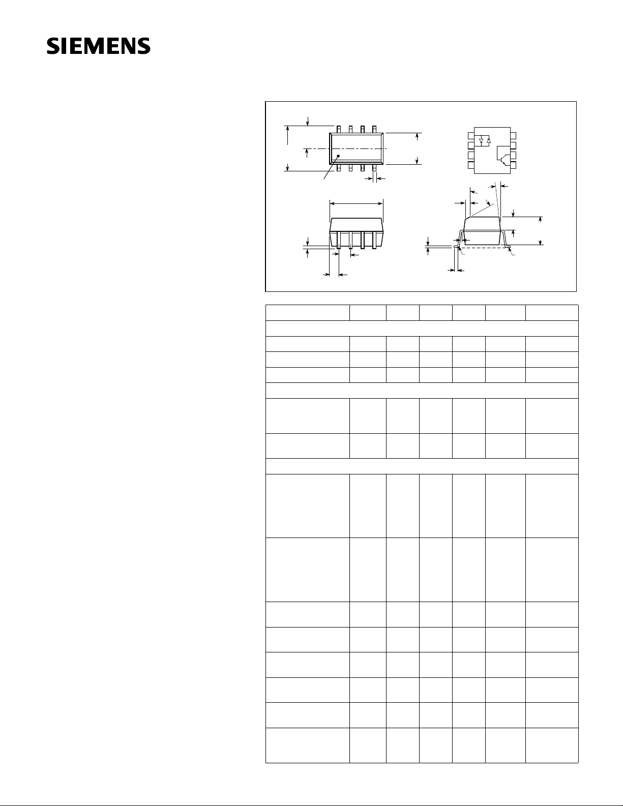
Dimensions in inches (mm)
40°
.240
(6.10)
.154±.005
(3.91±.13)
.050 (1.27)
typ.
.016 (.41)
.192±.005
(4.88±.13)
.004 (.10)
.008 (.20)
Lead
Coplanarity
±.0015 (.04)
max.
.015±.002
(.38±.05)
.008 (.20)
7°
.058±.005
(1.49±.13)
.125±.005
(3.18±.13)
Pin One ID
.120±.005
(3.05±.13)
C
L
.021 (.53)
5° max.
R.010
(.25) max.
.020±.004
(.15±.10)
2 plcs.
1
2
3
4
8
7
6
5
NC
Base
Collector
Emitter
Anode/
Cathode
Cathode/
Anode
NC
NC
IL205A/206A/207/208A
SMALL OUTLINE SURFACE MOUNT
PHOTOTRANSISTOR OPTOCOUPLER
 Loading...