


S102T02
S102T02 Series
S202T02 Series
■ Features
IT(rms)≤2A, Zero Cross type
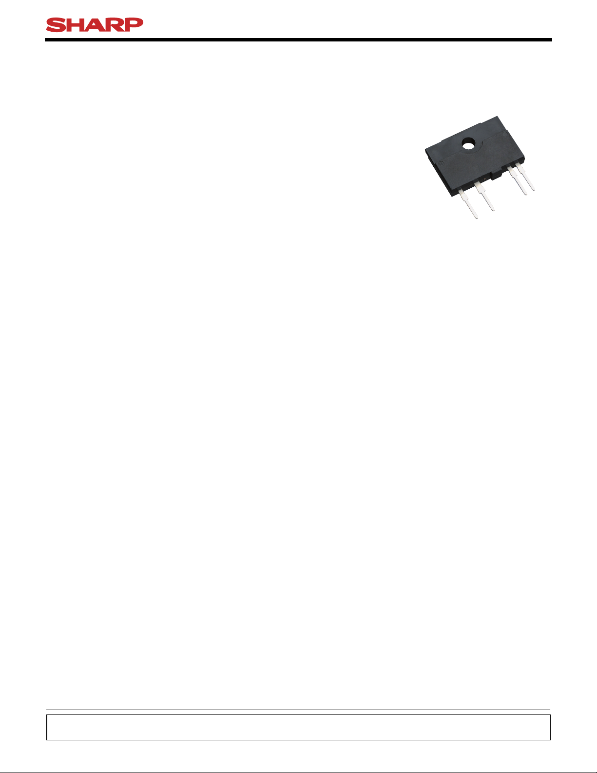
Low profile SIP 4pin
Triac output SSR
1. Output current, IT(rms)≤2.0A
2. Zero crossing functionary (VOX : MAX. 35V)
3. Slim 4 pin low profile SIP package
4. High repetitive peak off-state voltage
(V
DRM
: 600V, S202T02 Series)
(V
DRM
: 400V, S102T02 Series)
5. High isolation voltage between input and output
(V
iso
(rms) : 3.0kV)
6. Lead-free terminal components are also available
(see Model Line-up section in this datasheet)
7. Screw hole for heat sink
■ Description
S102T02 Series and S202T02 Series Solid State
Relays (SSR) are an integration of an infrared emitting
diode (IRED), a Phototriac Detector and a main output
Triac. These devices are ideally suited for controlling
high voltage AC loads with solid state reliability while
providing 3.0kV isolation (V
iso(rms)
) from input to out-
put.
1
Notice The content of data sheet is subject to change without prior notice.
In the absence of confirmation by device specification sheets, SHARP takes no responsibility for any defects that may occur in equipment using any SHARP
devices shown in catalogs, data books, etc. Contact SHARP in order to obtain the latest device specification sheets before using any SHARP device.
S102T02 Series
S202T02 Series
■ Agency approvals/Compliance
1. Isolated interface between high voltage AC devices
and lower voltage DC control circuitry.
2. Switching motors, fans, heaters, solenoids, and
valves.
3. Power control in applications such as lighting and
temperature control equipment.
■ Applications
1.
Recognized by UL508, file No. E94758 (as models No.
S102T02/S202T02)
2. Approved by CSA 22.2 No.14, file No. LR63705 (as
models No.
S102T02/S202T02
)
3. Package resin : UL flammability grade (94V-0)
Sheet No.:D4-A01601EN
Date Apr. 28. 2004
© SHARP Corporation
∗
Non-zero cross type is also available. (S102T01 Series/
S202T01 Series)
∗
: Do not allow external connection.
( ) : Typical dimensions
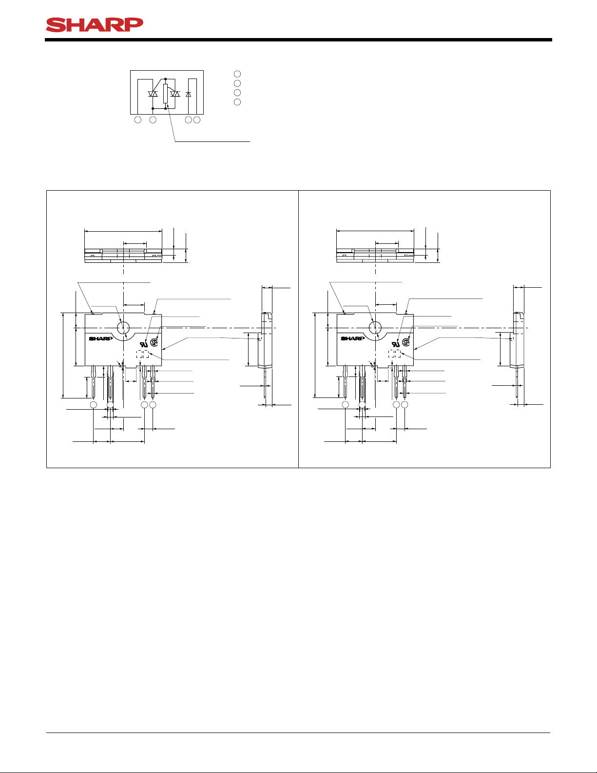
■ Internal Connection Diagram
1
1 2 3 4
2
3
4
Output (Triac T1)
Output (Triac T2)
Input (+)
Input (−)
Zero Crossing Circuit
2
■ Outline Dimensions
(Unit : mm)
S102T02
∗
~
+ −
S102T02
2A125VAC
23
±0.2
3
±0.2
0.4
±0.1
6.4
±0.2
1.6
±0.2
1.8
±0.3
φ3.7
±0.2
7
±0.2
4.5
±0.3
11.5
±0.2
10
±0.2
Common to pin No.2
Common to pin No.2
UL mark
CSA mark
Epoxy resin
Date code (2 digit)
6.2
MIN.
3.8
MIN.
0.2
MIN.
(3.8)
(5.08) (10.16)
(2.54)
1 2 3 4
3-1.2
±0.2
3-1.4
±0.2
4-0.8
±0.2
(3.5)
(0.8)
(1.8)
(25.8)
4
±0.2
1.8
±0.2
S202T02
∗
~
+ −
S202T02
2A265VAC
23
±0.2
3
±0.2
0.4
±0.1
6.4
±0.2
1.6
±0.2
1.8
±0.3
φ3.7
±0.2
7
±0.2
4.5
±0.3
11.5
±0.2
10
±0.2
Common to pin No.2
Common to pin No.2
UL mark
CSA mark
Epoxy resin
Date code (2 digit)
6.2
MIN.
3.8
MIN.
0.2
MIN.
(3.8)
(5.08) (10.16)
(2.54)
1 2 3 4
3-1.2
±0.2
3-1.4
±0.2
4-0.8
±0.2
(3.5)
(0.8)
(1.8)
(25.8)
4
±0.2
1.8
±0.2
S102T02 Series
S202T02 Series
Sheet No.: D4-A01601EN
Product mass : approx. 3.5g Product mass : approx. 3.5g
Date code (2 digit)
Rank mark
There is no rank mark indicator and currently there are no rank offered for this device.
A.D.
1990
1991
1992
1993
1994
1995
1996
1997
1998
1999
2000
2001
Mark
A
B
C
D
E
F
H
J
K
L
M
N
Mark
P
R
S
T
U
V
W
X
A
B
C
Mark
1
2
3
4
5
6
7
8
9
O
N
D
Month
January
February
March
April
May
June
July
August
September
October
November
December
A.D
2002
2003
2004
2005
2006
2007
2008
2009
2010
2011
2012
·
·
·
·
·
·
2nd digit
Month of production
1st digit
Year of production
Country of origin
Japan
3
repeats in a 20 year cycle
S102T02 Series
S202T02 Series
Sheet No.: D4-A01601EN
■ Electro-optical Characteristics
Parameter Symbol Unit
Input
Output
(Ta=25˚C)
Forward voltage
Reverse current
Repetitive peak OFF-state current
ON-state voltage
Holding current
Critical rate of rise of OFF-state voltage
Critical rate of rise of OFF-state voltage at commutaion
Minimum trigger current
Zero cross voltage
Isolation resistance
Turn-on time
Turn-off time
V
F
I
R
I
DRM
VT(rms)
I
H
dV/dt
(dV/dt)c
I
FT
V
OX
R
ISO
t
on
t
off
V
µA
µA
V
mA
V/µs
V/µs
mA
V
Ω
ms
ms
I
F
=20mA
V
R
=3V
V
D=VDRM
IT(rms)=2A, Resistance load, IF=20mA
−
V
D
=2/3•V
DRM
Tj=125˚C, VD=2/3•V
DRM
, dIT/dt=−1.0A/ms
VD=6V, RL=30Ω
I
F
=8mA
DC500V, 40 to 60%RH
VD(rms)=100V, AC50Hz, IF=20mA
IT(rms)=2A, Resistance load
VD(rms)=200V, AC50Hz, IF=20mA
IT(rms)=2A, Resistance load
VD(rms)=100V, AC50Hz, IF=20mA
IT(rms)=2A, Resistance load
VD(rms)=200V, AC50Hz, IF=20mA
IT(rms)=2A, Resistance load
Conditions MIN. TYP. MAX.
Transfer
charac-
teristics
S102T02
S202T02
S102T02
S202T02
−
−
−
−
−
30
4
−
−
10
10
−
−
−
−
1.2
−
−
−
−
−
−
−
−
−
−
−
−
−
1.4
100
100
1.7
25
−
−
8
35
−
10
10
10
10
■ Absolute Maximum Ratings
4
Parameter Symbol Rating Unit
Input
Output
(Ta=25˚C)
Forward current
Reverse voltage
RMS ON-state current
Peak one cycle surge current
Repetitive
peak OFF-state voltage
Non-Repetitive
peak OFF-state voltage
Critical rate of rise of ON-state current
Operating frequency
Isolation voltage
Operating temperature
Storage temperature
Soldering temperature
*2
*1
I
F
V
R
IT(rms)
I
surge
VDRM
VDSM
dIT/dt
f
V
iso
(rms)
T
opr
T
stg
T
sol
mA
V
A
A
V
V
A/µs
Hz
kV
˚C
˚C
˚C
*3
*3
*4
50
6
2
20
400
600
400
600
40
45 to 65
3.0
−25 to +100
−30 to +125
260
*1 40 to 60%RH, AC for 1minute, f=60Hz
*2 For 10s
*3 Refer to Fig.1, Fig.2
*4 f=60Hz sine wave, T
j
=25˚C start
S102T02
S202T02
S102T02
S202T02
S102T02 Series
S202T02 Series
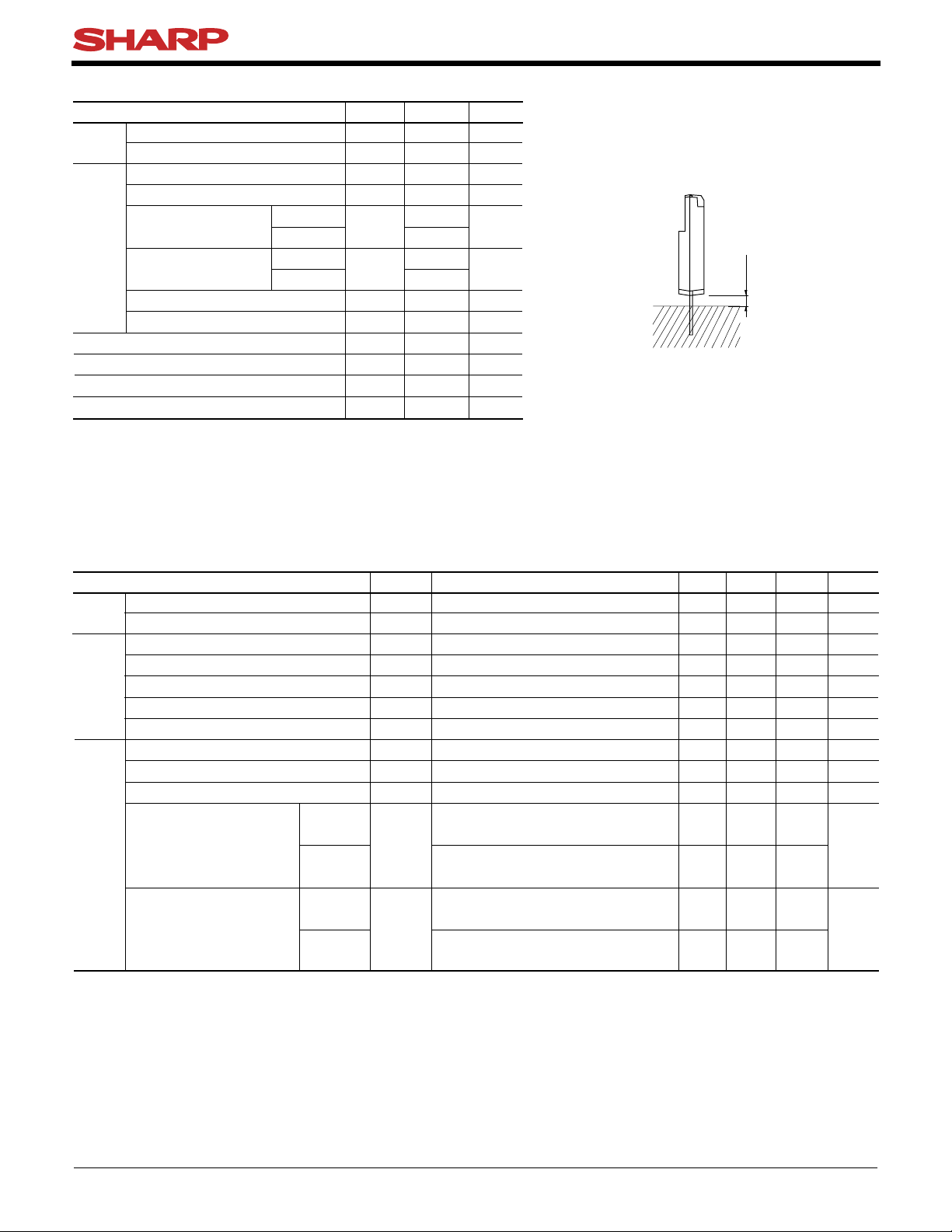
Soldering area
1.5mm
Sheet No.: D4-A01601EN
 Loading...