


SERVICE MANUAL
ER-A310
ER-A330
CODE: 00ZERA310USME
ELECTRONIC CASH REGISTER
ER-A310 MODEL ER-A330
SRV Key : LKGIM7113RCZZ PRINTER : ER-A310 : CR-510
ER-A330 : UCR-812A (For "U" & "A" version)
CONTENTS
CHAPTER 1. SPECIFICATIONS . . . . . . . . . . . . . . . . . . . . . . . . . . . . . . . . . . . . . 1
CHAPTER 2. OPTIONS . . . . . . . . . . . . . . . . . . . . . . . . . . . . . . . . . . . . . . . . . . . 6
CHAPTER 3. SRV. RESET AND MASTER RESET . . . . . . . . . . . . . . . . . . . . . . 6
CHAPTER 4. HARDWARE DESCRIPTION . . . . . . . . . . . . . . . . . . . . . . . . . . . . 7
CHAPTER 5. TEST FUNCTION . . . . . . . . . . . . . . . . . . . . . . . . . . . . . . . . . . . . 16
CHAPTER 6. CIRCUIT DIAGRAM & PWB LAYOUT . . . . . . . . . . . . . . . . . . . . 20
PARTS GUIDE
Parts marked with "!" is important for maintaining the safety of the set. Be sure to replace these parts with specified ones for maintaining the safety and performance of the set.
This document has been published to be used
SHARP CORPORATION for after sales service only.
The contents are subject to change without notice.

CHAPTER 1. SPECIFICATIONS
1. Appearance/Rating
1) Appearance
1 ER-A310
Journal paper
Printer cover |
Receipt paper |
Customer display (Pop-up type)
Operator display
Mode switch
Keyboard
Drawer
Drawer lock
2 ER-A330
Journal paper
Customer display (Pop-up type)
Printer cover
Operator display
Receipt paper
Mode switch
Keyboard
Drawer
Drawer lock
2) Rating
|
ER-A310 |
ER-A330 |
|
|
|
|
|
Power source |
120V AC ± 10%, 50/60 Hz |
||
|
|
|
|
Power |
Stand-by: 10W |
Stand-by: 10W |
|
consumption |
Operating: 31W (Max.) |
Operating: 38W (Max.) |
|
|
|
|
|
Operating |
32˚F to 104˚F (0˚C to 40˚C) |
||
temperature |
|||
|
|
||
|
|
|
|
Operating |
10% to 90% (RH) |
||
humidity |
|||
|
|
||
|
|
|
|
Physical |
420 (W) × 423 (D) × |
420 (W) × 423 (D) × |
|
dimensions, |
304 (H) mm |
314 (H) mm |
|
including the |
(16.5 (W) × 16.7 (D) × |
(16.5 (W) × 16.7 (D) × |
|
drawer |
12.0 (H) in.) |
12.4 (H) in.) |
|
|
|
|
|
Weight |
12.5 kg (27.6 lbs.) |
13.5 kg (30.0 lbs.) |
|
|
|
|
|
– 1 –

2. Keyboard
1) Standard keyboard layout
1 ER-A310
|
|
|
|
|
|
PLU/SUB |
|
NS |
|
|
|
|
|
|
|
X |
3 |
8 |
|
|
|
CL |
7 |
8 |
9 |
|
|
|
|
RECE IPT JOURNAL |
C |
|
|
7 |
|||||
|
|
|
|
|
|||||
RCPT PRINT |
@ |
4 |
5 |
6 |
|
|
|
||
FOR |
- |
2 |
6 |
||||||
|
|
|
|
|
|||||
RA |
|
RFND |
1 |
2 |
3 |
|
|
|
|
RM |
|
|
|
5 |
|||||
|
|
|
|
|
|
|
|||
PO |
% |
VOID |
0 |
00 |
• |
+ |
|
|
|
CAL |
1 •€ 4 |
||||||||
|
|
|
|
|
|||||
|
|
|
Dummy key |
|
Dummy key |
|
|
||
ESC AUTO
CH CONV
MDSE
SBTL CHK
#/TM/SBTL |
CA/AT |
= |
 Dummy key
2 ER-A330 |
|
|
|
|
|
|
|
|
|
|||
|
|
|
|
|
|
CASH PLU |
NS |
ESC |
FS |
FS |
||
|
|
|
|
|
|
# |
SUB |
SHIFT TEND |
||||
|
|
|
|
|
|
|
|
|
RA |
CH1 |
CH2 |
|
|
|
|
|
|
|
|
5 |
10 RM |
||||
|
|
|
|
|
|
|
|
|
||||
|
|
CL |
7 |
8 |
9 |
|
|
|
PO |
MDSE |
CHK |
|
RECE IPT JOURNAL |
C |
|
|
|
•€ |
4 |
9 |
CAL |
SBTL |
|
||
RCPT PRINT |
@ |
4 |
5 |
6 |
|
|
|
CONV |
#/TM/SBTL |
|||
FOR |
X |
3 |
8 |
|||||||||
|
|
|
|
|
|
|
|
|||||
1 |
2 |
RFND |
1 |
2 |
3 |
|
|
|
AUTO |
|
|
|
- |
2 |
7 |
1 |
|
|
|||||||
|
|
|
|
|
|
CA/AT |
||||||
|
|
|
|
|
|
|
|
|
AUTO |
|||
%1 |
%2 |
VOID |
0 |
00 |
• |
|
|
|
|
|
||
+ |
1 |
6 |
2 |
= |
|
|||||||
|
|
|
|
|
|
|
||||||
Dummy key |
|
Dummy key |
|
2) Key top name
1 Standard key top
KEY TOP |
DESCRIPTION |
ER-A310 |
ER-A330 |
|
|
|
|
|
|
- RECEIPT |
Receipt paper feed key |
è |
è |
|
- JOURNAL |
Journal paper feed key |
è |
è |
|
0~9,00 |
Numeric keys |
è |
è |
|
× |
Decimal point key |
è |
è |
|
@/FOR |
Multiplication key |
è |
è |
|
CL/C |
Clear key |
è |
è |
|
Validation print key |
è |
è |
||
Dept.1/+ |
Department 1/Plus key |
è |
è |
|
Dept.2/– |
Department 2/Minus key |
è |
è |
|
Dept.3/´ |
Department 3/ |
è |
è |
|
Multiplication key |
||||
|
|
|
||
|
|
|
|
|
Dept.4/¸ |
Department 4/Division key |
è |
è |
|
Dept.5~8 |
Department 5~8 keys |
è |
É |
|
Dept.5~10 |
Department 5~10 keys |
É |
è |
|
PLU/SUB |
PLU/Subdepartment key |
è |
è |
|
ESC |
Error escape key |
è |
è |
|
CASH# |
Cashier number entry key |
É |
è |
|
RCPT |
Receipt print key |
è |
è |
|
d |
Discount key |
è |
É |
|
d1, 2 |
Discount 1 and 2 keys |
É |
è |
|
AUTO |
Automatic sequencing key |
è |
É |
|
AUTO1, 2 |
Automatic sequencing 1 |
É |
è |
|
and 2 keys |
||||
|
|
|
||
|
|
|
|
|
% |
Percent key |
è |
É |
KEY TOP |
DESCRIPTION |
|
ER-A310 |
ER-A330 |
|
|
|
|
|
|
|
%1, 2 |
Percent 1 and 2 keys |
|
É |
|
è |
NS |
No-sale key |
|
è |
|
è |
RA/RM |
Received on account/ |
|
è |
|
è |
Recall memory key |
|
|
|||
|
|
|
|
|
|
|
|
|
|
|
|
PO/CAL |
Paid out/ |
|
è |
|
è |
Calculation mode key |
|
|
|||
|
|
|
|
|
|
|
|
|
|
|
|
RFND |
Refund key |
|
è |
|
è |
VOID |
Void key |
|
è |
|
è |
CH |
Charge key |
|
è |
|
É |
CH1, 2 |
Charge 1 and 2 keys |
|
É |
|
è |
CHK |
Check key |
|
è |
|
è |
CONV |
Conversion key |
|
è |
|
è |
MDSE SBTL |
Merchandise subtotal key |
|
è |
|
è |
#/TM/SBTL |
Non-add code/Time display/ |
|
è |
|
è |
Subtotal key |
|
|
|||
|
|
|
|
|
|
|
|
|
|
|
|
CA/AT /= |
Cash/Amount tendered/ |
|
è |
|
è |
Equals key |
|
|
|||
|
|
|
|
|
|
|
|
|
|
|
|
FS SHIFT |
Food stamp shift key |
|
É |
|
è |
FS TEND |
Food stamp tender key |
|
É |
|
è |
2 Optional key top |
|
|
|
|
|
|
|
|
|
|
|
KEY TOP |
DESCRIPTION |
ER-A310 |
|
ER-A330 |
|
|
|
|
|
|
|
Dept. 9~30 |
Department 9~30 keys |
è |
|
É |
|
Dept. 11~50 |
Department 11~50 keys |
É |
|
è |
|
DEPT# |
Department number |
è |
|
è |
|
entry key |
|
||||
|
|
|
|
|
|
|
|
|
|
|
|
TAX1 |
Tax1 ~ Tax4 shift keys |
|
|
|
|
SHIFT~TAX4 |
|
è |
|
è |
|
SHIFT |
|
|
|
|
|
|
|
|
|
|
|
TAX |
Manual tax key |
è |
|
è |
|
AUTO2 |
Automatic sequencing 2 |
è |
|
É |
|
key |
|
||||
|
|
|
|
|
|
|
|
|
|
|
|
AUTO3, 4 |
Automatic sequencing 3 |
É |
|
è |
|
and 4 keys |
|
||||
|
|
|
|
|
|
|
|
|
|
|
|
CONV2~4 |
Conversion 2~4 keys |
è |
|
è |
|
CA2 |
Cash total 2 key |
è |
|
è |
|
CH2 |
Charge 2 key |
è |
|
É |
|
d2 |
Discount 2 key |
è |
|
É |
|
%2 |
Percent 2 key |
è |
|
É |
|
– 2 –
4. Display
1) Operator display
PLU/SUB
DEPT REPEAT
RCPT
OFF
 : This appears when a transaction is finalized.
 : This appears when the cash register computes the subtotal.
: This appears when the chage due amount is displayed.
: This appears when the batteries are iow.
DISPLAY DEVICE |
LED |
|
|
NUMBER OF LINE |
1 line |
|
|
NUMBER OF POSITIONS |
10 positions |
|
|
COLOR OF DISPLAY |
Green |
|
|
CHARACTER SIZE |
14.2mm (H) × 8.0mm (H) |
|
|
2) Customer display (Pop-up type)
DISPLAY DEVICE |
LED |
|
|
NUMBER OF LINE |
1 line |
|
|
NUMBER OF POSITIONS |
7 positions |
|
|
COLOR OF DISPLAY |
Green |
|
|
CHARACTER SIZE |
14.2mm (H) × 8.0mm (H) |
|
|
3) Lamps
|
DISPLAY |
DESCRIPTION |
|
POSITION |
|
|
|
|
|
|
|
AMOUNT |
1 8 |
|
|
|
|
MINUS SIGN |
4 10 |
: Floating |
|
|
|
ERROR |
10 |
|
|
|
|
PGM MODE |
10 |
|
|
|
|
CA/AT |
10 |
: Lights up when a |
NS |
|
registration is finalized by |
CH |
|
depressing CA/AT, NS, |
CHK |
|
CH or CHK key |
|
|
|
SUBTOTAL/ |
10 |
|
SHORT TENDER |
|
|
|
|
|
CHANGE |
10 |
: Lights up whenever the |
|
|
change due amount |
|
|
appears in the display. |
|
|
|
DEPARTMENT |
9 10 |
No zero-suppressed. |
|
|
|
PLU |
8 10 |
No zero-suppressed. |
|
|
|
REPEAT |
8 |
Endless count, starting from 2. |
|
|
|
DECIMAL POINT |
3 1 |
TAB |
|
|
|
LOW BATTERY |
10 |
: Light up when the voltage |
|
|
of the battery for memory |
|
|
retention is lower than the |
|
|
regulated voltage. |
|
|
(The voltage is checked |
|
|
when "POWER ON" or |
|
|
"Batteries are |
|
|
exchanged".) |
|
|
|
RECEIPT OFF |
8 |
— |
|
|
|
CASHIER No. |
2 3 |
– || – : 01 06 code entry |
|
|
|
VALIDATION |
10 |
: Light up when the |
|
|
validation printing is |
|
|
compulsory. |
|
|
|
CONVERSION or |
10 |
|
CALC. MODE |
|
|
|
|
|
– 3 –

5. Printer
1) Printer specifications
ITEMS |
|
|
|
|
|
|
|
ER-A310 |
|
|
|
|
|
|
|
|
|
|
|
|
|
ER-A330 |
|
|
|
|
|
||
|
|
|
|
|
|
|
|
|
|
|
|
|
|
|
|
|
|
|
|
|
|
|
|
|
|
|
|
|
|
Model name |
CR-510 |
|
|
|
|
|
|
|
|
|
|
|
|
UCR-812A |
|
|
|
|
|
|
|
|
|
|
|
|
|||
|
|
|
|
|
|
|
|
|
|
|
|
|
|
|
|
|
|
|
|
|
|
|
|
|
|
|
|
|
|
No. of station |
2 (Receipt/Journal) |
|
|
|
|
|
|
|
|
|
2 (Receipt/Journal) |
|
|
|
|
|
|
|
|
||||||||||
|
|
|
|
|
|
|
|
|
|
|
|
|
|
|
|
|
|
|
|
|
|
|
|
|
|
|
|||
Printing system |
Inner hammer, rubber character selection type |
|
|
|
Print wheel selective type |
|
|
|
|
|
|
|
|||||||||||||||||
|
|
|
|
|
|
|
|
|
|
|
|
|
|
|
|
|
|
|
|
|
|
|
|
|
|
|
|
||
Printing capacity |
Receipt |
|
: Max. 12 chr. |
|
|
|
|
|
|
Receipt |
|
|
: Max. 10 chr. |
|
|
|
|
|
|||||||||||
|
Journal |
|
: Max. 12 chr. |
|
|
|
|
|
|
Journal |
|
|
: Max. 10 chr. |
|
|
|
|
|
|||||||||||
|
Validation |
|
: Max. 24 chr./1 line |
|
|
|
|
|
Validation |
|
|
: Max. 20 chr./1 line |
|
|
|
|
|||||||||||||
|
|
|
|
|
|
|
|
|
|
|
|
|
|
|
|
|
|
|
|
|
|
|
|
|
|
|
|
||
Character size |
1.8mm (W) ´ 2.7mm (H) |
|
|
|
|
|
|
|
|
Figure |
|
|
: 1.7mm (W) ´ 3.2mm (H) |
|
|
||||||||||||||
|
|
|
|
|
|
|
|
|
|
|
|
|
|
|
|
Symbol |
|
|
: 2.4mm (W) ´ 3.2mm (H) |
|
|
||||||||
|
|
|
|
|
|
|
|
|
|
|
|
|
|
|
|
|
|
|
|
|
|
|
|
|
|
|
|
||
Print pitch |
Column distance : 2.8mm |
|
|
|
|
|
|
|
Column distance |
: 3.35mm for between 1st and 2nd |
|||||||||||||||||||
|
|
|
|
|
|
|
|
|
|
|
|
|
|
|
|
|
|
|
|
column 3.0mm for after 3rd column |
|||||||||
|
Row distance |
: 4.3mm |
|
|
|
|
|
|
|
Row distance |
: 5.1mm |
|
|
|
|
|
|
||||||||||||
|
|
|
|
|
|
|
|
|
|
|
|
|
|
|
|
|
|
|
|
|
|
|
|
|
|
|
|
|
|
Print speed |
Approx. 3.0 lines/sec. |
|
|
|
|
|
|
|
|
|
Approx. 2.6 lines/sec. |
|
|
|
|
|
|
|
|
||||||||||
|
|
|
|
|
|
|
|
|
|
|
|
|
|
|
|
|
|
|
|
|
|
|
|
|
|
|
|||
Paper feed speed |
Approx. 29 lines/sec. at receipt issued. |
|
|
|
|
|
Approx. 18 lines/sec. at receipt issued. |
|
|
|
|
||||||||||||||||||
|
|
|
|
|
|
|
|
|
|
|
|
|
|
|
|
|
|
|
|
|
|
|
|
|
|
|
|
|
|
Reliability |
MCBF 2.5 million lines |
|
|
|
|
|
|
|
|
|
MCBF 2 million lines |
|
|
|
|
|
|
|
|
||||||||||
|
|
|
|
|
|
|
|
|
|
|
|
|
|
|
|
|
|
|
|
|
|
|
|
|
|
|
|
|
|
Validation form sensor |
No |
|
|
|
|
|
|
|
|
|
|
|
|
|
No |
|
|
|
|
|
|
|
|
|
|
|
|
||
|
|
|
|
|
|
|
|
|
|
|
|
|
|
|
|
|
|
|
|
|
|
|
|
|
|
|
|
|
|
Near end sensor |
Journal side: No |
|
|
|
|
|
|
|
|
|
Journal side: No |
|
|
|
|
|
|
|
|
|
|
||||||||
|
Receipt side: No |
|
|
|
|
|
|
|
|
|
Receipt side: No |
|
|
|
|
|
|
|
|
|
|
||||||||
|
|
|
|
|
|
|
|
|
|
|
|
|
|
|
|
|
|
|
|
|
|
|
|
|
|
|
|
|
|
Cutter |
Manual |
|
|
|
|
|
|
|
|
|
|
|
|
Manual |
|
|
|
|
|
|
|
|
|
|
|
|
|||
|
|
|
|
|
|
|
|
|
|
|
|
|
|
|
|
|
|
|
|
|
|
|
|
|
|
|
|||
Print wheel layout |
Parts code: 00BM755001010 |
|
|
|
|
|
|
|
Parts code: 00BM712002300 |
|
|
|
|
|
|
||||||||||||||
|
12 |
11 |
10 |
9 |
|
8 |
7 |
6 |
5 |
4 |
3 |
2 |
1 |
|
10 |
9 |
|
8 |
|
7 |
6 |
5 |
4 |
3 |
2 |
1 |
|
||
|
|
|
|
|
|
|
|
|
|
|
|
|
|
|
|
|
|
|
|
|
|
|
|
|
|
|
|
|
|
|
|
PL |
|
GT |
|
|
– |
|
– |
|
– |
|
CA |
|
|
|
PL |
Z |
|
TX |
. |
. |
. |
. |
GT |
CA |
@ |
|
|
|
|
|
|
|
|
|
|
|
|
|
|
|
|
|
|
|
|
|
|
|
|
|
|
|
|
|
|
||
|
|
0 |
0 |
0 |
0 |
|
0 |
0 |
0 |
0 |
0 |
CD |
CH |
1¤2 |
|
|
– |
– |
– |
– |
– |
– |
– |
# |
CK |
Q |
|
||
|
|
1 |
1 |
1 |
1 |
|
1 |
1 |
1 |
1 |
1 |
P |
CK |
1 |
|
|
|
|
|
|
|
|
|
% |
CH |
CG |
|
||
|
|
|
|
|
|
|
|
|
|
|
|
|
|
|
|
|
|
|
|
|
|
|
|
|
|
|
|
|
|
|
|
2 |
2 |
2 |
2 |
|
2 |
2 |
2 |
2 |
2 |
X |
CR |
2 |
|
|
|
|
|
|
|
|
|
|
|
|
|
|
|
|
|
|
|
|
|
|
|
|
|
|
|
|
|
|
|
|
|
|
|
|
|
|
|
|
|
|
|
|
|
|
|
3 |
3 |
3 |
3 |
|
3 |
3 |
3 |
3 |
3 |
Z |
EX |
3 |
|
|
0 |
0 |
|
0 |
|
0 |
0 |
0 |
0 |
0 |
RA |
TD |
|
|
|
|
|
|
|
|
|
|
|
|
|
|
|
|
|
|
|
|
|
|
|
|
|
|
|
|
|
|
|
|
|
4 |
4 |
4 |
4 |
|
4 |
4 |
4 |
4 |
4 |
# |
TX |
4 |
|
|
1 |
1 |
|
1 |
|
1 |
1 |
1 |
1 |
1 |
PO |
1 |
|
|
|
5 |
5 |
5 |
5 |
|
5 |
5 |
5 |
5 |
5 |
RF |
FS |
5 |
|
|
2 |
2 |
|
2 |
|
2 |
2 |
2 |
2 |
2 |
VD |
2 |
|
|
|
|
|
|
|
|
|
|
|
|
|
|
|
|
|
|
|
|
|
|
|
|
|
|
|
|
|
|
|
|
|
6 |
6 |
6 |
6 |
|
6 |
6 |
6 |
6 |
6 |
VD |
% |
6 |
|
|
3 |
3 |
|
3 |
|
3 |
3 |
3 |
3 |
3 |
NS |
3 |
|
|
|
|
|
|
|
|
|
|
|
|
|
|
|
|
|
|
|
|
|
|
|
|
|
|
|
|
|
|
|
|
|
7 |
7 |
7 |
7 |
|
7 |
7 |
7 |
7 |
7 |
TR |
d |
7 |
|
|
4 |
4 |
|
4 |
|
4 |
4 |
4 |
4 |
4 |
TX |
4 |
|
|
|
8 |
8 |
8 |
8 |
|
8 |
8 |
8 |
8 |
8 |
Q |
RA |
CG |
|
|
5 |
5 |
|
5 |
|
5 |
5 |
5 |
5 |
5 |
FS |
5 |
|
|
|
|
|
|
|
|
|
|
|
|
|
|
|
|
|
|
|
|
|
|
|
|
|
|
|
|
|
|
|
|
|
9 |
9 |
9 |
9 |
|
9 |
9 |
9 |
9 |
9 |
@ |
PO |
TD |
|
|
6 |
6 |
|
6 |
|
6 |
6 |
6 |
6 |
6 |
d |
6 |
|
|
|
|
|
|
|
|
|
|
|
|
|
|
|
|
|
|
|
|
|
|
|
|
|
|
|
|
|
|
|
|
|
|
|
|
|
|
|
|
|
|
+ |
NS |
TL |
|
|
7 |
7 |
|
7 |
|
7 |
7 |
7 |
7 |
7 |
X |
1¤2 |
|
|
|
|
– |
– |
– |
– |
. |
. |
. |
. |
No |
– |
* |
ST |
|
|
8 |
8 |
|
8 |
|
8 |
8 |
8 |
8 |
8 |
EX |
ST |
|
|
|
|
|
|
|
|
|
|
|
|
|
|
|
|
|
|
|
|
|
|
|
|
|
|
|
|
|
|
|
|
|
|
|
|
|
|
|
|
|
|
|
|
|
|
|
|
|
9 |
9 |
|
9 |
|
9 |
9 |
9 |
9 |
9 |
RF |
TL |
|
|
|
|
|
|
|
|
|
|
|
|
|
|
|
|
|
|
|
|
|
|
|
|
|
|
|
|
|
|
|
|
|
|
|
|
|
|
|
|
|
|
|
|
|
|
|
|
|
|
|
|
|
|
|
|
|
|
|
|
|
2) Roll paper
Parts code |
DPAPR1006CSZZ |
|
Dimension |
44.5±0.5mm in width |
|
|
Max. 83mm in diameter |
|
|
|
|
Paper quality |
Journal/Receipt |
|
|
Fine quality paper |
|
|
Paper thickness |
: 0.06 to 0.09 mm |
|
Paper weight |
: 52.3 to 64g/m2 |
|
Validation form |
|
|
Normal paper only |
|
|
Thickness |
: 0.09 to 0.14 mm |
|
Size |
: 110mm or more, 210mm or |
under (W) ´ 70mm or more (H)
– 4 –
3) Validation paper
ER-A310 |
ER-A330 |
Paper quality Normal paper only |
Normal paper and pressure sensitive paper only |
Thickness : 0.09 to 0.14 mm |
Thickness : 0.07 to 0.14 mm |
Size : 110 mm or more, 210 mm or under (W) × 70 mm or more (H) |
Size : 115 mm or more (W) × 70 mm or more (H) |
|
|
Printing area |
|
|
76.2 |
14.2 |
|
29.4 |
19.1 |
29.4 |
16 |
|
|
|
|
|
|
|
|
32.6 |
(11) |
32.6 |
|
|
|
|
|
|
|
|
9.3 |
10Dig. |
|
10Dig. |
16.6 |
|
|
|
|
|
|
|
|
|
|
|
|
Wide over 115mm |
|
||
4) Inking
|
ER-A310 |
ER-A330 |
|
|
|
Parts code |
NROLR6652RCZZ |
NROLR6638RCZZ |
|
|
|
Ink supply system |
Ink roller |
Ink roller |
|
|
|
Form |
Roller |
Roller |
|
|
|
Specification |
Material-rubber |
Material-rubber |
|
|
|
Roller life |
Approx. 0.4 million lines |
Approx. 0.6 million lines |
|
|
|
Print color |
Purple |
Purple |
|
|
|
5) Logo stamp
|
ER-A310 |
ER-A330 |
|
|
|
Material |
Porous rubber |
Porous rubber |
|
|
|
Size |
30mm (W) × 20mm (H) |
30mm (W) × 20mm (H) |
|
|
|
Color |
Purple |
Purple |
|
|
|
Parts code for ink |
UINK1001CCZZ |
UINK1001CCZZ |
|
|
|
6. Drawer
1) Drawer box and drawer
Model name |
SK423 |
|
|
Size |
420(W) × 423(D) × 112(H) mm |
|
|
Color |
Light olive gray |
|
|
Material |
Metal |
|
|
Bell |
— |
|
|
Release lever |
Standard equipment; Situated at the bottom |
|
|
Drawer open sensor |
Standard equipment |
|
|
2) Money case
|
For "U" version |
For "A" version |
|
|
|
Separation from the drawer |
Allowed |
Allowed |
|
|
|
Separation of the coin |
Disallowed |
Disallowed |
compartments from the |
|
|
money case |
|
|
|
|
|
Bill separator |
— |
Yes |
|
|
|
Number of compartments |
5B/5C |
4B/8C |
|
|
|
Bill compartments
Bill separator
Coin compartments |
5B/5C |
4B/8C |
3) Lock
Location of the lock |
Front |
|
|
|
|
Method of locking |
Locking |
: Insert the drawer lock key |
and unlocking |
|
into the lock and turn it 90 |
|
|
degrees counterclockwise. |
|
|
|
|
Unlocking |
: Insert the drawer lock key |
|
|
into the lock and turn it 90 |
|
|
degrees clockwise. |
|
|
|
Key No. |
SK1-1 |
|
|
|
|
7. Memory back up
For memory back up, the dry battery ULM-3 (3 pieces) is needed.
1. Memory holding time: Approximate 1 year after NEW dry batteries are inserted.
2. Battery exchange method: When the low battery symbol "L" lights up, batteries (3 pieces) exchange by the following method, within 2 days.
1) Power on the ECR.
2) Turn the MODE SW to "OP X/Z" mode.
3) Release the OLD dry batteries (3 pieces).
4) Insert the NEW dry batteries (3 pieces).
5) Confirm the low battery symbol "L" lights off.
– 5 –

CHAPTER 2. OPTIONS
1. Sales options
No. |
NAME |
MODEL |
DESCRIPTIONS |
|
|
|
|
|
|
1 |
REMOTE DRAWER |
ER-04DW |
5B/5C |
|
|
|
|
|
|
2 |
COIN CASE |
ER-55C2 |
5B/5C |
|
|
|
|
|
|
3 |
KEY TOP KIT |
ER-11KT7 |
1 |
× 1 key top |
|
|
|
|
|
|
|
ER-12KT7 |
1 |
× 2 key top |
|
|
|
|
|
|
|
ER-22KT7 |
2 |
× 2 key top |
|
|
|
|
|
|
|
ER-11DK7 |
1 |
× 1 dummy key |
|
|
|
|
|
|
|
ER-51DK7 |
5 |
× 1 dummy key |
|
|
|
|
|
2. Service options
No. |
NAME |
PARTS CODE |
PRICE RANK |
DESCRIPTIONS |
|
|
|
|
|
1 |
SRV KEY |
LKGIM7113RCZZ |
AK |
|
|
|
|
|
|
2 |
MODE KEYGRIP COVER |
LKGIM7126RCZZ |
AL |
OP key only |
|
|
|
|
|
3 |
DRIP-PROOF KEYBOARD COVER |
GCÇVH7126BHZZ |
BE |
|
|
|
|
|
|
4 |
SHIELD PLATE KIT |
DKIT-8666BHZZ |
BL |
Only for ER-A330 |
|
|
|
|
|
3. Supplies
No. |
NAME |
PARTS CODE |
PRICE RANK |
DESCRIPTIONS |
|
|
|
|
|
1 |
ROLL PAPER |
DPAPR1006CSZZ |
AR |
|
|
|
|
|
|
2 |
INK ROLLER (ER-A310) |
NRÇLR6652RCZZ |
AZ |
|
|
|
|
|
|
3 |
INK ROLLER (ER-A330) |
NRÇLR6638RCZZ |
AY |
|
|
|
|
|
|
4 |
INK FOR STAMP |
UINK-1001CCZZ |
AK |
|
|
|
|
|
|
CHAPTER 3. SRV RESET AND MASTER RESET
The SRV key is used for operating in the SRV mode.
1. SRV. reset (Program Loop Reset)
Used to return the machine back to its operational state after a lockup has occurred.
Procedure
• Method 1
1)Turn off the AC switch.
2)Set the mode switch to (SRV′) position.
3)Turn on the AC switch.
4)Turn to (SRV) position from (SRV′) position.
2. Master reset (All memory clear)
There are two possible methods to perform a master reset.
• MRS-1
Used to clear all memory contents and return machine back to its initial settings. return keyboard back to default. for default keyboard layout.
Procedure-1 (with SRV key)
1)Unplug the AC cord from the wall outlet.
2)Set the MODE switch to the (SRV′) position.
3)Plug in the AC cord to the wall outlet.
4)While holding down JOURNAL FEED key, turn to (SRV) position from (SRV′) position.
Procedure-2 (without SRV key)
1)Turn the mode switch to the (REG) position.
2)Ensure the batteries are not installed in the battery compartment and insert the plug into the outlet.
3)The right most decimal point will blink for a few seconds.
4)The register will sound three beeps.
5) The register will display " |
." |
– 6 –

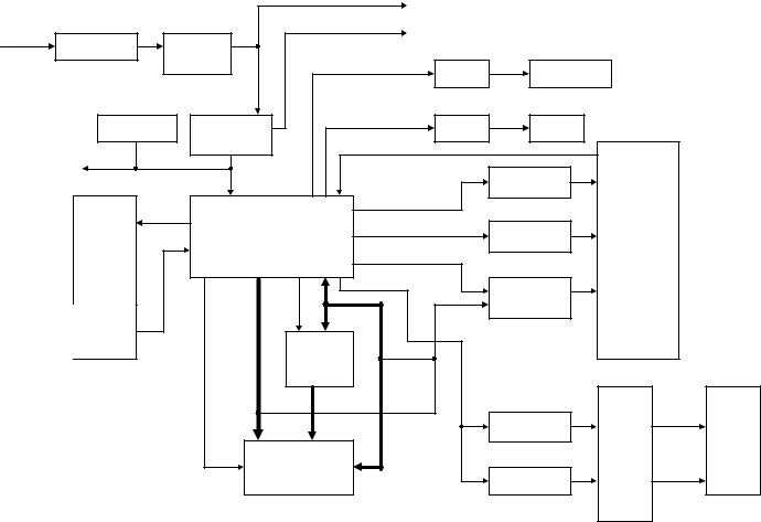
CHAPTER 4. HARDWARE DESCRIPTION
1. Block diagram
1) ER-A310
|
|
|
|
PRINTER POWER SOURCE : +24V |
|
|
|
|
|
|
|
DISPLAY POWER SOURCE : +5.5V |
|
|
|
TRANSFORMER |
VOLTAGE |
|
|
|
|
|
|
|
REGULATOR |
|
DRIVE SIGNAL |
|
|
|
|
|
|
|
|
DRAWER |
|
|
|
|
|
|
|
DRIVER |
|
|
|
DRY BATTERY |
DC-DC |
|
DRIVE SIGNAL |
BUZZER |
|
|
|
|
DRIVER |
|
|
||||
|
|
CONVERTER |
TIMING SIGNAL |
|
|
|
|
|
|
|
|
|
|
|
|
|
|
|
|
|
STEP MOTOR |
|
|
|
|
|
|
|
DRIVER |
|
|
|
STROBE |
|
|
DRIVE SIGNAL |
|
|
|
|
|
|
|
|
|
|
|
|
SIGNAL |
|
|
|
|
|
|
|
|
|
CPU |
DRIVE SIGNAL |
STAMP, PAPER |
PRINTER |
|
KEYBOARD |
|
|
|
FEED DRIVER |
|
||
|
µPD78045 |
|
|
||||
8X9 72KEY |
|
|
|
HAMMER COMMON SIGNAL |
|
CR-510 |
|
|
|
|
|
|
|
||
|
|
|
|
|
|
|
|
|
|
|
LATCH |
DRIVE SIGNAL |
HAMMER MG |
|
|
|
|
|
SIGNAL |
DRIVER |
|
|
|
|
|
|
|
|
|
||
|
|
|
|
|
|
|
|
MODE |
|
|
|
|
|
|
|
SWITCH |
RETURN |
|
|
|
|
|
|
8SIGNAL |
|
|
|
|
|
|
|
SIGNAL |
|
ADDRESS |
|
|
|
||
|
|
|
|
|
|||
|
|
|
LATCH |
|
|
|
|
|
|
ADDRESS |
ADDRESS |
DATA BUS |
|
|
|
|
|
BUS |
BUS |
|
|
|
|
|
|
|
|
|
|
||
|
|
|
|
|
SEGMENT |
|
POP-UP |
CHIP SELECTSIGNAL |
|
|
DRIVER |
OP. |
DISPLAY |
||
|
|
|
7SEG LED |
||||
|
|
|
|
|
|
DISPLAY |
|
|
|
|
|
|
|
7DIG |
|
|
|
|
S-RAM |
|
|
7SEG LED |
|
|
|
|
|
|
|
||
|
|
|
256 kbit |
|
DIGIT DRIVER |
10DIG |
|
|
|
|
|
|
|
|
|
|
|
|
|
DIGIT SIGNAL |
|
|
|
– 7 –
2) ER-A330 |
|
|
|
|
|
|
|
|
|
|
|
PRINTER POWER SOURCE : +18V |
|
|
|
|
|
|
|
DISPLAY POWER SOURCE : +5.5V |
|
|
|
TRANSFORMER |
VOLTAGE |
|
|
|
|
|
|
|
REGULATOR |
|
DRIVE SIGNAL |
|
|
|
|
|
|
|
|
DRAWER |
|
|
|
|
|
|
|
DRIVER |
|
|
|
DRY BATTERY |
DC-DC |
|
DRIVE SIGNAL |
BUZZER |
|
|
|
|
DRIVER |
|
|
||||
|
|
CONVERTER |
TIMING SIGNAL |
|
|
|
|
|
|
|
|
|
|
|
|
|
|
|
|
|
STEP MOTOR |
|
|
|
|
|
|
|
DRIVER |
|
|
|
STROBE |
|
|
DRIVE SIGNAL |
|
|
|
|
|
|
|
|
|
|
|
|
SIGNAL |
|
|
|
|
|
|
|
|
|
CPU |
DRIVE SIGNAL |
STAMP, PAPER |
PRINTER |
|
KEYBOARD |
|
|
|
FEED DRIVER |
|
||
|
µPD78045 |
|
|
||||
8X9 72KEY |
|
|
|
HAMMER COMMON SIGNAL |
|
UCR-812A |
|
|
|
|
|
|
|
||
|
|
|
|
|
|
|
|
|
|
|
LATCH |
DRIVE SIGNAL |
PRINT WHEEL |
|
|
|
|
|
SIGNAL |
MG DRIVER |
|
|
|
|
|
|
|
|
|
||
|
|
|
|
|
|
|
|
MODE |
|
|
|
|
|
|
|
SWITCH |
RETURN |
|
|
|
|
|
|
8SIGNAL |
|
|
|
|
|
|
|
SIGNAL |
|
ADDRESS |
|
|
|
||
|
|
|
|
|
|||
|
|
|
LATCH |
|
|
|
|
|
|
ADDRESS |
ADDRESS |
DATA BUS |
|
|
|
|
|
BUS |
BUS |
|
|
|
|
|
|
|
|
|
|
||
|
|
|
|
|
SEGMENT |
|
POP-UP |
CHIP SELECTSIGNAL |
|
|
DRIVER |
OP. |
DISPLAY |
||
|
|
|
7SEG LED |
||||
|
|
|
|
|
|
DISPLAY |
|
|
|
|
|
|
|
7DIG |
|
|
|
|
S-RAM |
|
|
7SEG LED |
|
|
|
|
|
|
|
||
|
|
|
256 kbit |
|
DIGIT DRIVER |
10DIG |
|
|
|
|
|
|
|
|
|
|
|
|
|
DIGIT SIGNAL |
|
|
|
– 8 –
2. CPU (UPD78045F) pin configuration
No. |
PIN NAME |
|
ER-A310 |
|
ER-A330 |
I/O |
ACTIVE |
|
|
|
|
||||
|
|
SIGNAL NAME |
DESCRIPTION |
SIGNAL NAME |
DESCRIPTION |
|
|
|
|
|
|
|
|
|
|
1 |
P94 |
DIG7 |
Display digit 7 |
DIG7 |
Display digit 7 |
O |
H |
|
|
|
|
|
|
|
|
2 |
P93 |
DIG6 |
Display digit 6 |
DIG6 |
Display digit 6 |
O |
H |
|
|
|
|
|
|
|
|
3 |
P92 |
DIG5 |
Display digit 5 |
DIG5 |
Display digit 5 |
O |
H |
|
|
|
|
|
|
|
|
4 |
P91 |
DIG4 |
Display digit 4 |
DIG4 |
Display digit 4 |
O |
H |
|
|
|
|
|
|
|
|
5 |
P90 |
DIG3 |
Display digit 3 |
DIG3 |
Display digit 3 |
O |
H |
|
|
|
|
|
|
|
|
6 |
P81 |
DIG2 |
Display digit 2 |
DIG2 |
Display digit 2 |
O |
H |
|
|
|
|
|
|
|
|
7 |
P80 |
DIG1 |
Display digit 1 |
DIG1 |
Display digit 1 |
O |
H |
|
|
|
|
|
|
|
|
8 |
VDD |
VDD |
+5V |
VDD |
+5V |
|
|
|
|
|
|
|
|
|
|
9 |
P27 |
AD7 |
RAM Address & Data bus 7 |
AD7 |
RAM Address & Data bus 7 |
I/O |
H |
|
|
|
|
|
Printer magnet 8 |
|
|
|
|
|
|
|
|
|
|
10 |
P26 |
AD6 |
RAM Address & Data bus 6 |
AD6 |
RAM Address & Data bus 6 |
I/O |
H |
|
|
|
|
|
Printer magnet 7 |
|
|
|
|
|
|
|
|
|
|
11 |
P25 |
AD5 |
RAM Address & Data bus 5 |
AD5 |
RAM Address & Data bus 5 |
I/O |
H |
|
|
|
Journal print magnet 6 |
|
Printer magnet 6 |
|
|
|
|
|
Receipt print magnet 6 |
|
|
|
|
|
|
|
|
|
|
|
|
12 |
P24 |
AD4 |
RAM Address & Data bus 4 |
AD4 |
RAM Address & Data bus 4 |
I/O |
H |
|
|
|
Journal print magnet 5 |
|
Printer magnet 5 |
|
|
|
|
|
Receipt print magnet 5 |
|
|
|
|
|
|
|
|
|
|
|
|
13 |
P23 |
AD3 |
RAM Address & Data bus 3 |
AD3 |
RAM Address & Data bus 3 |
I/O |
H |
|
|
|
Journal print magnet 4 |
|
Printer magnet 4 |
|
|
|
|
|
Receipt print magnet 4 |
|
|
|
|
|
|
|
|
|
|
|
|
14 |
P22 |
AD2 |
RAM Address & Data bus 2 |
AD2 |
RAM Address & Data bus 2 |
I/O |
H |
|
|
|
Journal print magnet 3 |
|
Printer magnet 3 |
|
|
|
|
|
Receipt print magnet 3 |
|
|
|
|
|
|
|
|
|
|
|
|
15 |
P21 |
AD1 |
RAM Address & Data bus 1 |
AD1 |
RAM Address & Data bus 1 |
I/O |
H |
|
|
|
Journal print magnet 2 |
|
Printer magnet 2 |
|
|
|
|
|
Receipt print magnet 2 |
|
|
|
|
|
|
|
|
|
|
|
|
16 |
P20 |
AD0 |
RAM Address & Data bus 0 |
AD0 |
RAM Address & Data bus 0 |
I/O |
H |
|
|
|
Journal print magnet 1 |
|
Printer magnet 1 |
|
|
|
|
|
Receipt print magnet 1 |
|
|
|
|
|
|
|
|
|
|
|
|
17 |
/RESET |
/RESET |
Reset signal |
/RESET |
Reset signal |
I |
L |
|
|
|
|
|
|
|
|
18 |
P74 |
SCOM |
Printer step motor common signal |
NU |
NU |
O |
H |
|
|
|
|
|
|
|
|
19 |
P73 |
SM4 |
Printer step motor drive signal 4 |
NU |
NU |
O |
H |
|
|
|
|
|
|
|
|
20 |
AVSS |
AVSS |
GND |
AVSS |
GND |
|
|
|
|
|
|
|
|
|
|
21 |
P17 |
KR11 |
Key return signal 11 |
KR11 |
Key return signal 11 |
I |
H |
|
|
|
|
|
|
|
|
22 |
P16 |
KR10 |
Key return signal 10 |
KR10 |
Key return signal 10 |
I |
H |
|
|
|
|
|
|
|
|
23 |
P15 |
KR9 |
Key return signal 9 |
KR9 |
Key return signal 9 |
I |
H |
|
|
|
|
|
|
|
|
24 |
P14 |
KR8 |
Key return signal 8 |
KR8 |
Key return signal 8 |
I |
H |
|
|
|
|
|
|
|
|
25 |
P13 |
KR7 |
Key return signal 7 |
KR7 |
Key return signal 7 |
I |
H |
|
|
|
|
|
|
|
|
26 |
P12 |
KR6 |
Key return signal 6 |
KR6 |
Key return signal 6 |
I |
H |
|
|
|
|
|
|
|
|
27 |
P11 |
KR5 |
Key return signal 5 |
KR5 |
Key return signal 5 |
I |
H |
|
|
|
|
|
|
|
|
28 |
P10 |
P10 |
Dry battery voltage |
P10 |
Dry battery voltage |
I |
|
|
|
|
|
|
|
|
|
29 |
AVDD |
AVDD |
+5V |
AVDD |
+5V |
|
|
|
|
|
|
|
|
|
|
30 |
AVREF |
AVREF |
+5V (VCC) |
AVREF |
+5V (VCC) |
|
|
|
|
|
|
|
|
|
|
31 |
XT1 |
XT1 |
Sub clock: 32.768 kHz |
P04 |
Sub clock: 32.768 kHz |
I |
|
|
|
|
|
|
|
|
|
32 |
XT2 |
XT2 |
|
XT2 |
|
O |
|
|
|
|
|
|
|
|
|
33 |
VSS |
VSS |
GND |
VSS |
GND |
|
|
|
|
|
|
|
|
|
|
34 |
X1 |
X1 |
Main clock: 4.19 MHz |
X1 |
Main clock: 4.19 MHz |
I |
|
|
|
|
|
|
|
|
|
35 |
X2 |
X2 |
|
X2 |
|
O |
|
|
|
|
|
|
|
|
|
36 |
P37 |
MD |
Printer motor ON signal |
MD |
Printer motor ON signal |
O |
H |
|
|
|
|
|
|
|
|
37 |
P36 |
BUZ |
Buzzer ON signal |
BUZ |
Buzzer ON signal |
O |
H/L |
|
|
|
|
|
|
|
|
38 |
P35 |
RF |
Receipt paper feed signal |
RF |
Receipt paper feed signal |
O |
H |
|
|
|
|
|
|
|
|
39 |
P34 |
JF |
Journal paper feed signal |
JF |
Journal paper feed signal |
O |
H |
|
|
|
|
|
|
|
|
40 |
P33 |
STAMP |
Stamp ON signal |
STAMP |
Stamp ON signal |
O |
H |
|
|
|
|
|
|
|
|
– 9 –
No. |
PIN NAME |
|
ER-A310 |
|
ER-A330 |
I/O |
ACTIVE |
|
|
|
|
|
|||||
|
|
SIGNAL NAME |
DESCRIPTION |
SIGNAL NAME |
DESCRIPTION |
|
|
|
|
|
|
|
|
|
|
|
|
41 |
P32 |
/ALE |
Address latch signal |
/ALE |
Address latch signal |
O |
↓ |
|
|
|
|
|
|
|
|
|
|
42 |
P31 |
/CE |
Chip select signal |
/CE |
Chip select signal |
O |
L |
|
|
|
|
|
|
|
|
|
|
43 |
P30 |
/WE |
Write signal |
/WE |
Write signal |
O |
L |
|
|
|
|
|
|
|
|
|
|
44 |
P03 |
RMS |
NU |
RMS |
NU |
I |
|
|
|
|
|
|
|
|
|
|
|
45 |
P02 |
R |
Printer reset signal |
DRS |
Drawer open sensor |
I |
|
|
|
|
|
|
|
|
|
|
|
46 |
P01 |
T |
Printer timing signal |
α |
Printer timing signal |
I |
− H |
|
|
|
|
|
|
|
|
|
|
47 |
P00 |
PE |
Power enable signal |
PE |
Power enable signal |
I |
H |
|
|
|
|
|
|
|
|
|
|
48 |
IC |
IC |
VSS |
IC |
VSS |
|
|
|
|
|
|
|
|
|
|
|
|
49 |
P72 |
SM3 |
Printer step motor drive signal 3 |
P72 |
NU |
O |
H |
|
|
|
|
|
|
|
|
|
|
50 |
P71 |
SM2 |
Printer step motor drive signal 2 |
MG10 |
Printer magnet 10 |
O |
H |
|
|
|
|
|
|
|
|
|
|
51 |
P70 |
SM1 |
Printer step motor drive signal 1 |
MG9 |
Printer magnet 9 |
O |
H |
|
|
|
|
|
|
|
|
|
|
52 |
VDD |
VDD |
+5V |
VDD |
+5V |
|
|
|
|
|
|
|
|
|
|
|
|
53 |
P127 |
DRS |
Drawer open sensor (input) |
R-COM |
Printer receipt common signal |
O |
H |
|
|
|
|
|
|
|
|
|
|
54 |
P126 |
HCOM |
Printer hammer common signal |
J-COM |
Printer journal common signal |
O |
H |
|
|
|
|
|
|
|
|
|
|
55 |
P125 |
J1 |
Mode signal (ER-A310: GND) |
J1 |
Mode signal (ER-A330: VDD) |
I |
H |
|
|
|
|
|
|
|
|
|
|
56 |
P124 |
DR1 |
Standard drawer drive signal |
DR1 |
Standard drawer drive signal |
O |
H |
|
|
|
|
|
|
|
|
|
|
57 |
P123 |
KR4 |
Key return signal 4 |
KR4 |
Key return signal 4 |
I |
H |
|
|
|
|
|
|
|
|
|
|
58 |
P122 |
KR3 |
Key return signal 3 |
KR3 |
Key return signal 3 |
I |
H |
|
|
|
|
|
|
|
|
|
|
59 |
P121 |
KR2 |
Key return signal 2 |
KR2 |
Key return signal 2 |
I |
H |
|
|
|
|
|
|
|
|
|
|
60 |
P120 |
KR1 |
Key return signal 1 |
KR1 |
Key return signal 1 |
I |
H |
|
|
|
|
|
|
|
|
|
|
61 |
P117 |
A14 |
RAM Address 14 |
A14 |
RAM Address 14 |
O |
|
|
|
|
|
|
|
|
|
|
|
62 |
P116 |
A13 |
RAM Address 13 |
A13 |
RAM Address 13 |
O |
|
|
|
|
|
|
|
|
|
|
|
63 |
P115 |
A12 |
RAM Address 12 |
A12 |
RAM Address 12 |
O |
|
|
|
|
|
|
|
|
|
|
|
64 |
P114 |
A11 |
RAM Address 11 |
A11 |
RAM Address 11 |
O |
|
|
|
|
|
|
|
|
|
|
|
65 |
P113 |
A10 |
RAM Address 10 |
A10 |
RAM Address 10 |
O |
|
|
|
|
|
|
|
|
|
|
|
66 |
P112 |
A9 |
RAM Address 9 |
A9 |
RAM Address 9 |
O |
|
|
|
|
|
|
|
|
|
|
|
67 |
P111 |
A8 |
RAM Address 8 |
A8 |
RAM Address 8 |
O |
|
|
|
|
|
|
|
|
|
|
|
68 |
P110 |
DR2 |
Option drawer drive signal |
DR2 |
Option drawer drive signal |
O |
H |
|
|
|
|
|
|
|
|
|
|
69 |
P107 |
DP/ST8 |
Display segment signal DP |
DP/ST8 |
Display segment signal DP |
O |
H |
|
Key strobe signal 8 |
Key strobe signal 8 |
|||||||
|
|
|
|
|
|
|||
|
|
|
|
|
|
|
|
|
70 |
P106 |
G/ST7 |
Display segment signal G |
G/ST7 |
Display segment signal G |
O |
H |
|
Key strobe signal 7 |
Key strobe signal 7 |
|||||||
|
|
|
|
|
|
|||
|
|
|
|
|
|
|
|
|
71 |
VLOAD |
VLOAD |
VSS |
VLOAD |
VSS |
|
|
|
|
|
|
|
|
|
|
|
|
72 |
P105 |
F/ST6 |
Display segment signal F |
F/ST6 |
Display segment signal F |
O |
H |
|
Key strobe signal 6 |
Key strobe signal 6 |
|||||||
|
|
|
|
|
|
|||
|
|
|
|
|
|
|
|
|
73 |
P104 |
E/ST5 |
Display segment signal E |
E/ST5 |
Display segment signal E |
O |
H |
|
Key strobe signal 5 |
Key strobe signal 5 |
|||||||
|
|
|
|
|
|
|||
|
|
|
|
|
|
|
|
|
74 |
P103 |
D/ST4 |
Display segment signal D |
D/ST4 |
Display segment signal D |
O |
H |
|
Key strobe signal 4 |
Key strobe signal 4 |
|||||||
|
|
|
|
|
|
|||
|
|
|
|
|
|
|
|
|
75 |
P102 |
C/ST3 |
Display segment signal C |
C/ST3 |
Display segment signal C |
O |
H |
|
Key strobe signal 3 |
Key strobe signal 3 |
|||||||
|
|
|
|
|
|
|||
|
|
|
|
|
|
|
|
|
76 |
P101 |
B/ST2 |
Display segment signal B |
B/ST2 |
Display segment signal B |
O |
H |
|
Key strobe signal 2 |
Key strobe signal 2 |
|||||||
|
|
|
|
|
|
|||
|
|
|
|
|
|
|
|
|
77 |
P100 |
A/ST1 |
Display segment signal A |
A/ST1 |
Display segment signal A |
O |
H |
|
Key strobe signal 1 |
Key strobe signal 1 |
|||||||
|
|
|
|
|
|
|||
|
|
|
|
|
|
|
|
|
78 |
P97 |
DIG10 |
Display digit signal 10 |
DIG10 |
Display digit signal 10 |
O |
H |
|
|
|
|
|
|
|
|
|
|
79 |
P96 |
DIG9 |
Display digit signal 9 |
DIG9 |
Display digit signal 9 |
O |
H |
|
|
|
|
|
|
|
|
|
|
80 |
P95 |
DIG8 |
Display digit signal 8 |
DIG8 |
Display digit signal 8 |
O |
H |
|
|
|
|
|
|
|
|
|
– 10 –
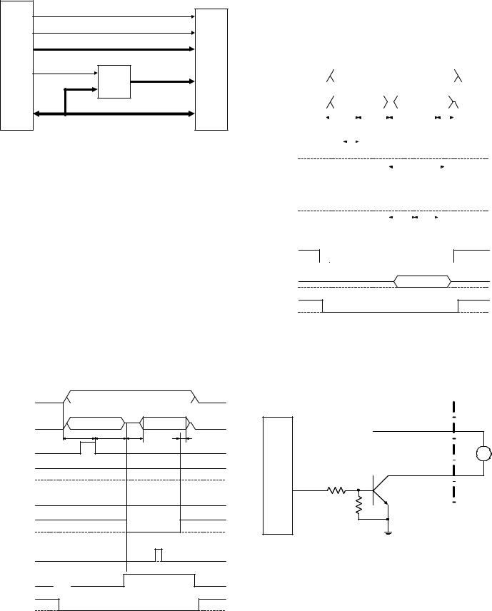
3. RAM control |
|
|
|
|
|
|
/CE |
|
|
|
|
/WE |
|
|
|
|
A8~A14 |
|
|
IC2 |
/ALE |
|
|
IC14 |
CPU |
|
|
||
|
|
IC3 |
A0~A7 |
S-RAM |
|
|
|
||
|
|
|
|
|
|
AD0~AD7 |
74HC373 |
|
|
|
|
|
AD0~AD7 |
|
/WE: |
Write signal |
|
When the signal is low, writing is performed. When the |
|
signal is high, reading is performed. |
/CE: |
Chip select signal |
A8-A14: |
Address bus |
AD0-7: |
Address/Data bus |
A0-1: |
Address bus signal |
/ALE: |
Address latch signal |
Address signals A0-A7 are used commonly with the data bus. When the address latch signal /ALE is input to IC3, the address/data bus signal AD0-AD7 access the RAM as address signals A0-A7.
(READ)
As shown in the attached time chart, address signals are outputted from P20-P27, P111-P117, and the lower address is latched with
P32. The modes at P20-P27 are changed to the input mode. The chip enable signal (P31) is output for the RAM. Then the output data from the RAM are read from P20-P27.
RAM control
(READ cycle)
P111~P117 |
Upper address |
|
|
P20~P27 |
Lower address |
RAM data output |
||
|
15ns or above |
0ns or above |
||
|
Lower address |
15ns or |
||
P32 |
70ns or above |
|||
latch signal |
above |
|||
|
||||
|
|
|||
30ns or above 

P30 RAM /WE Fixed to HIGH.
RAM /OE Fixed to LOW
P31 RAM /CS
P20~P27 READ timing
70ns or above 

Input
P20~P27 Select
Output
Hammer common
(WRITE)
As shown in the attached time chart, address signals are outputted from P20-P27, P111-P117, and the lower address is latched with P32. The write enable signal (P30) is output. The write data to the RAM are output from P20-P27. Then the chip enable signal (P31) is output to write the data.
RAM control
(WRITE cycle)
|
|
|
|
|
|
|
|
|
|
|
|
|
|
|
|
|
|
|
|
|
P111~P117 |
Upper address |
|
|
|
|
|
|
|
|
|
|
|
|
|
||||||
|
|
|
|
|
|
|
|
|
|
|
|
|
|
|
|
|
|
|
|
|
|
|
|
|
|
|
|
|
|
|
|
|
|
|
|
|
|
|
|||
P20~P27 |
|
|
|
Lower address |
|
|
|
|
Input data to RAM |
|
||||||||||
|
|
|
|
|
|
|
|
|
|
|
|
|
|
|
|
|
|
|||
|
|
|
15ns or above |
|
|
|
|
|
30ns or above |
|
|
|
|
|
|
|
||||
|
|
|
|
|
|
|
|
|
|
|
|
|
|
|||||||
|
Lower address |
|
|
15ns or |
|
|
|
|
|
|
|
|
|
|
|
|
|
|||
P32 |
|
|
|
|
|
|
|
|
0ns or above |
|||||||||||
latch signal |
|
|
above |
|
|
|
|
|
|
|||||||||||
|
|
|
|
|
|
|
|
|
|
|
|
|
|
|
||||||
|
|
|
|
|
|
|
|
|
|
|
|
|
|
|
|
|||||
|
|
30ns or above |
|
|
|
|
|
|
|
|
|
|
|
|
|
|
|
|||
|
|
|
|
|
|
|
|
|
|
|
|
|
|
|
|
|
||||
|
|
|
|
|
|
|
|
|
|
|
|
|
|
|
|
|
|
|
|
|
P30 |
RAM /WE |
|
|
|
|
|
|
|
|
|
|
|
|
|
|
|
|
|||
|
|
|
|
|
|
|
|
|
|
|
|
|
|
|
|
|
||||
|
|
|
|
|
|
|
|
|
|
|
|
50ns or above |
|
|
||||||
RAM /OE |
Fixed to LOW. |
|
|
|
|
|
|
|
|
|
|
|
|
|
|
|
|
|||
|
|
|
|
|
|
|
|
|
|
|
|
|
|
|
|
|||||
|
|
|
|
|
|
|
|
|
|
|
|
|
|
|
|
|
|
|
|
|
|
|
|
|
|
|
|
|
|
|
|
|
|
|
|
|
|
|
|
|
|
P20~P27 |
RAM /CS |
|
|
|
|
|
|
|
|
|
|
|
|
|
|
|
|
|||
|
|
|
|
|
|
|
|
|
|
|
|
|
|
|
|
|||||
|
|
|
|
|
|
|
|
|
|
|
|
|
|
|
||||||
P20~P27 |
|
|
|
|
|
|
|
|
|
0ns or |
60ns or |
|
|
|||||||
READ timing |
|
|
|
|
|
|
above |
above |
||||||||||||
|
|
|
|
|
|
|
|
|
|
|
|
|
|
|
|
|
|
|
|
|
Input
P20~P27 Select


 Output


RAM Data IN
Hammer common
4. Printer control circuit (ER-A310)
1) Printer motor drive circuit
VP : +24V
M
Q17
C3784
IC2
CPU
R60
MD
R61
The motor drive signal MD from the CPU is used to operate the printer motor with switching operation of transistor Q17.
– 11 –
 Loading...