


SGS Thomson Microelectronics HCC4056BM1, HCC4056BF, HCC4056BEY, HCC4056BC1, HCC4055BM1 Datasheet
...HCC4054B/55B/56B
HCF4054B/55B/56B
LIQUID-CRYSTAL DISPLAY DRIVERS
4054B 4-SEGMENT DISPLAY DRIVER - STROBED LATCH FUNCTION
4055B BCD TO 7-SEGMENT DECODER/DRIVER, WITH ºDIS- PLAY-FREQUENCYº OUTPUT
4056B
.QUIESCENT CURRENT SPECIFIED TO 20V
.FOR HCC DEVICE
OPERATION OF LIQUID CRYSTALS WITH COS/MOS CIRCUITS PROVIDES ULTRA-
.LOW-POWER DISPLAYS
EQUIVALENT AC OUTPUT DRIVE FOR LI- QUID-CRYSTAL DISPLAYS-NO EXTERNAL
.CAPACITOR REQUIRED
VOLTAGE DOUBLING ACROSS DISPLAY [(VDD ± VEE) = 18V)] RESULTS IN EFFECTIVE 36V (p-p) DRIVE ACROSS SELECTED DIS-
.PLAY SEGMENTS
LOW-OR HIGH-OUTPUT LEVEL DC DRIVE
.FOR OTHER TYPES OF DISPLAYS
ON-CHIP LOGIC-LEVEL CONVERSION FOR DIFFERENT INPUT AND OUTPUT-LEVEL
.SWINGS
FULL DECODING OF ALL INPUT COMBINATIONS : º0 ± 9, L, H, P, A± º AND BLANK POSI-
.TIONS
INPUT CURRENT OF 100nA AT 18V AND 25°C
.FOR HCC DEVICE
.100% TESTED FOR QUIESCENT CURRENT MEETS ALL REQUIREMENTS OF JEDECTENTATIVE STANDARD N°. 13A, ºSTANDARD SPECIFICATIONS FOR DESCRIPTION OF ºBº SERIES CMOS DEVICESº
DESCRIPTION
The HCC4054B, HCC4055B and HCC4056B (extended temperature range) and the HCF4054B, HCF4055B and HCF4056B (intermediate temperature range) are monolithic integrated circuits available in 16-lead dual in-line plastic or ceramic package and plastic micro package. The HCC/HCF4055B and HCC/HCF4056B types are single-digit BCD-to-7-seg- ment decoder/driver circuits that provide level-shifting functions on the chip. This feature permits the BCD input-signal swings (VDD to VSS) to be the same as
EY |
F |
(Plastic Package) |
(Ceramic Frit Seal Package) |
M1 |
C1 |
(Micro Package) |
(Plastic Chip Carrier) |
ORDER CODES :
HCC40XXBF HCF40XXBM1
HCF40XXBEY HCF40XXBC1
or different from the 7-segment output-signal swings (VDD to VEE). For example, the BCD input-signal swings (VDD to VSS) may be as low as 0 to ± 3V, whereas the output-display drive-signal swing (VDD to VEE) may be from 0 to ± 5V. If VDD to VEE exceeds 15V, VDD to VSS should be at least 4V. The 7-seg- ment outputs are controlled by the DISPLAY-FRE- QUENCY (DF) input which causes the selected segment outputs to be low, high, or a square-wave output (for liquid-crystal displays). When the DF input is low the output segments will be high when selected by the BCD inputs. When the DF input is high, the output segments will be low when selected by the BCD inputs. When a square-wave is present at the DF input, the selected segments will have a square-wave output that is 180° out of phase with the DF input. Those segments which are not selected will have a square-wave output that is in phase with the input. DF square-wave repetition rates for liquid-crystal displays usually range from 30Hz (well above flicker rate) to 200Hz (well below the upper limit of the liquid-crystal frequency response). The HCC/HCF4055B provides a levelshifted high-amplitude DF output which is required for driving the common electrode in liquid-crystal displays. The HCC/HCF4056B provides a strobedlatch function at the BCD inputs. Decoding of all input combinations on the HCC/HCF4055B and HCC/HCF4056B provides displays of 0 to 9 as well
March 1989 |
1/15 |
HCC/HCF4054B/55B/56B
as L, P, H, A,± , and a blank position. (see typical application for other letters). The HCC/HCF4054B provides level shifting similar to the HCC/HCF4055B and HCC/HCF4056B independently strobed latches, and common DF control on 4 signal lines. The HCC/HCF4054B is intended to provide drive-signal compatibility with the HCC/HCF4055B and HCC/HCF4056B 7-segment decoder types for the decimal point, colon, polarity, and similar display lines. A level-shifted high-amplitude DF output can be obtained from any HCC/HCF4054B output line by connecting the corresponding input and strobe lines to a low and high level, respectively. The HCC/HCF4054B may also be utilized for logic-level ºup conversionº or ºdown conversionº. Forexample, input-signal swings (VDD to VSS) from + 5 to 0V can be converted to output-signal swings (VDD to VEE) of + 5 to ± 5V. The level-shifted function on all three types permits the use of different input-and outputsignal swings. The input swings from a low level of VSS to a high level of VDD while the output swings
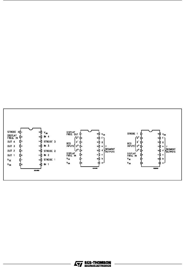
PIN CONNECTIONS
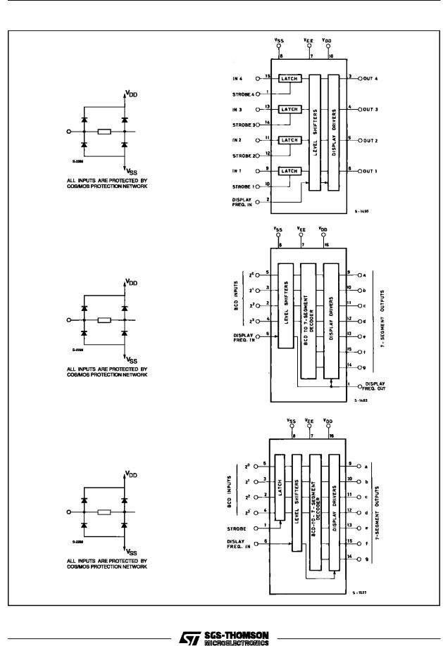
from a low level of VEE to the same high level of VDD. Thus, the input and output swings can be selected independently of each other over a 3-to-18V range. VSS may be connected to VEE when no level-shift function is required. For the HCC/HCF 4054B and HCC/HCF 4056B, data are transferred from input to output by placing a high voltage level at the strobe input. A low voltage level at the strobe input latches the data input and the corresponding output segments remain selected (or non-selected) while the strobe is low. Whenever the level-shifting function is required, the HCC/HCF4055B can be used by itself to drive a liquid-crystal display (fig. 10 and fig. 12). The HCC/HCF4056B, however, must be used together with a HCC/HCF4054B to provide the common DF output (fig. 14). The capability of extending the voltage swing on the negative end (this voltage cannot be extended on the positive end) can be used to advantage in the set-up of fig. 11. Fig. 9 is common to all three types.
4054B |
4055B |
4056B |
2/15
HCC/HCF4054B/55B/56B
FUNCTIONAL DIAGRAMS
4054B
4055B
4056B
3/15
HCC/HCF4054B/55B/56B
ABSOLUTE MAXIMUM RATINGS
Symbol
V DD*
Vi
II
Pt o t
T o p
Ts t g
Parameter |
Value |
Unit |
Supply Voltage : HC C Types |
± 0.5 to + 20 |
V |
H C F Types |
± 0.5 to + 18 |
V |
Input Voltage |
± 0.5 to VDD + 0.5 |
V |
DC Input Current (any one input) |
± 10 |
mA |
Total Power Dissipation (per package) |
200 |
mW |
Dissipation per Output Transistor |
|
|
for To p = Full Package-temperature Range |
100 |
mW |
Operating Temperature : HCC Types |
± 55 to + 125 |
°C |
H CF Types |
± 40 to + 85 |
°C |
Storage Temperature |
± 65 to + 150 |
°C |
Stresses above those listed under ºAbsolute Maximum Ratingsº may cause permanent damage to the device. This is a stress rating only and functional operation of the device at these or any other conditions above those indicated in the operational sections of this specification is not implied. Exposure to absolute maximum rating conditions for external periods may affect device reliability.
* All voltage values are referred to VSS pin voltage.
RECOMMENDED OPERATING CONDITIONS
Symbol |
Parameter |
Value |
Unit |
VDD |
Supply Voltage : H CC Types |
3 to 18 |
V |
|
H C F Types |
3 to 15 |
V |
V I |
Input Voltage |
0 to VDD |
V |
T o p |
Operating Temperature : HCC Types |
± 55 to 125 |
°C |
|
HC F Types |
± 40 to 85 |
°C |
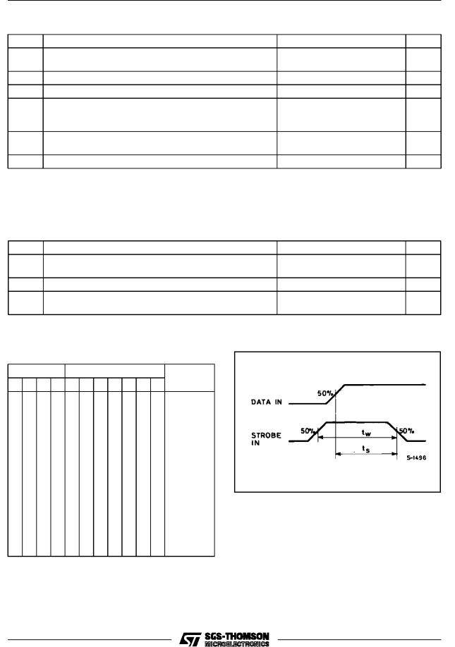
TRUTH TABLE
Data Setup Time and Strobe Pulse Duration.
4055 B and 4056 B
Input Code |
|
|
Output State |
|
|
Display |
|||||
23 22 21 |
20 |
a |
b |
c |
d |
e |
f |
g |
Character |
||
0 |
0 |
0 |
0 |
1 |
1 |
1 |
1 |
1 |
1 |
0 |
0 |
0 |
0 |
0 |
1 |
0 |
1 |
1 |
0 |
0 |
0 |
0 |
1 |
0 |
0 |
1 |
0 |
1 |
1 |
0 |
1 |
1 |
0 |
1 |
2 |
0 |
0 |
1 |
1 |
1 |
1 |
1 |
1 |
0 |
0 |
1 |
3 |
0 |
1 |
0 |
0 |
0 |
1 |
1 |
0 |
0 |
1 |
1 |
4 |
0 |
1 |
0 |
1 |
1 |
0 |
1 |
1 |
0 |
1 |
1 |
5 |
0 |
1 |
1 |
0 |
1 |
0 |
1 |
1 |
1 |
1 |
1 |
6 |
0 |
1 |
1 |
1 |
1 |
1 |
1 |
0 |
0 |
0 |
0 |
7 |
1 |
0 |
0 |
0 |
1 |
1 |
1 |
1 |
1 |
1 |
1 |
8 |
1 |
0 |
0 |
1 |
1 |
1 |
1 |
1 |
0 |
1 |
1 |
9 |
1 |
0 |
1 |
0 |
0 |
0 |
0 |
1 |
1 |
1 |
0 |
L |
1 |
0 |
1 |
1 |
0 |
1 |
1 |
0 |
1 |
1 |
1 |
H |
1 |
1 |
0 |
0 |
1 |
1 |
0 |
0 |
1 |
1 |
1 |
P |
1 |
1 |
0 |
1 |
1 |
1 |
1 |
0 |
1 |
1 |
1 |
A |
1 |
1 |
1 |
0 |
0 |
0 |
0 |
0 |
0 |
0 |
1 |
± |
1 |
1 |
1 |
1 |
0 |
0 |
0 |
0 |
0 |
0 |
0 |
BLANK |
4/15

HCC/HCF4054B/55B/56B
STATIC ELECTRICAL CHARACTERISTICS (over recommended operating conditions)
Test Conditions |
Value |
Symbol |
Parameter |
|
IL |
Quiescent |
|
|
Supply |
HCC |
|
Current |
|
|
|
Types |
|
|
HCF |
|
|
Types |
VOH |
Output High |
|
|
Voltage |
|
VOL |
Output Low |
|
|
Voltage |
|
VIH |
Input High |
|
|
Voltage |
|
VIL |
Input Low |
|
|
Voltage |
|
IOH |
Output |
HCC |
|
High |
|
|
Current |
Types |
|
|
HCF |
|
|
Types |
IOL |
Output |
HCC |
|
Low |
|
|
Current |
Types |
|
|
HCF |
|
|
Types |
IIH, IIL** |
Input |
HCC |
|
Leakage |
Types |
|
Current |
HCF |
|
|
|
|
|
Types |
CI** |
Input Capacitance |
|
VEE |
VI |
VO |
VSS |
VDD |
TLow* |
|
25°C |
|
THi gh* |
(V) |
(V) |
(V) |
(V) |
(V) |
Min. Max. Min. Typ. Max. Min. Max. |
||||
|
|
|
|
|
|||||
± 5 |
0/5 |
|
0 |
5 |
5 |
|
0.04 |
5 |
150 |
0 |
0/10 |
|
0 |
10 |
10 |
|
0.04 |
10 |
300 |
0 |
0/15 |
|
0 |
15 |
20 |
|
0.04 |
20 |
600 |
0 |
0/20 |
|
0 |
20 |
100 |
|
0.08 |
100 |
3000 |
± 5 |
0/5 |
|
0 |
5 |
20 |
|
0.04 |
20 |
150 |
0 |
0/10 |
|
0 |
10 |
40 |
|
0.04 |
40 |
300 |
0 |
0/15 |
|
0 |
15 |
80 |
|
0.04 |
80 |
600 |
0 |
0/5 |
|
0 |
5 |
4.95 |
4.95 |
|
|
4.95 |
0 |
0/10 |
|
0 |
10 |
9.95 |
9.95 |
|
|
9.95 |
0 |
0/15 |
|
0 |
15 |
14.95 |
14.95 |
|
|
14.95 |
0 |
5/0 |
|
0 |
5 |
0.05 |
|
|
0.05 |
0.05 |
0 |
10/0 |
|
0 |
10 |
0.05 |
|
|
0.05 |
0.05 |
0 |
15/0 |
|
0 |
15 |
0.05 |
|
|
0.05 |
0.05 |
± 5 |
|
0.5/4.5 |
0 |
5 |
3.5 |
3.5 |
|
|
3.5 |
0 |
|
1/9 |
0 |
10 |
7 |
7 |
|
|
7 |
0 |
|
1.5/13.5 |
0 |
15 |
11 |
11 |
|
|
11 |
5 |
|
0.5/4.5 |
0 |
5 |
1.5 |
|
|
1.5 |
1.5 |
0 |
|
9/1 |
0 |
10 |
3 |
|
|
3 |
3 |
0 |
|
1.5/13.5 |
0 |
15 |
4 |
|
|
4 |
4 |
± 5 |
0/5 |
4.5 |
0 |
5 |
± 0.6 |
± 0.45 |
± 0.9 |
|
± 0.3 |
0 |
0/10 |
9.5 |
0 |
10 |
± 0.6 |
± 0.45 |
± 0.9 |
|
± 0.3 |
0 |
0/15 |
13.5 |
0 |
15 |
± 1.9 |
± 1.5 |
± 3 |
|
± 1.1 |
± 5 |
0/5 |
4.5 |
0 |
5 |
± 0.47 |
± 0.38 |
± 0.9 |
|
± 0.28 |
0 |
0/10 |
9.5 |
0 |
10 |
± 0.47 |
± 0.38 |
± 0.9 |
|
± 0.28 |
0 |
0/15 |
13.5 |
0 |
15 |
± 1.58 |
± 1.27 |
± 3 |
|
± 0.95 |
± 5 |
0/5 |
0.4 |
0 |
5 |
1.6 |
1.3 |
2.6 |
|
0.9 |
0 |
0/10 |
0.5 |
0 |
10 |
1.6 |
1.3 |
2.6 |
|
0.9 |
0 |
0/15 |
1.5 |
0 |
15 |
4.2 |
3.4 |
6.8 |
|
2.4 |
± 5 |
0/5 |
0.4 |
0 |
5 |
1.37 |
1.1 |
2.6 |
|
0.82 |
0 |
0/10 |
0.5 |
0 |
10 |
1.37 |
1.1 |
2.6 |
|
0.82 |
0 |
0/15 |
1.5 |
0 |
15 |
3.62 |
2.9 |
6.8 |
|
2.17 |
0 |
0/18 |
|
0 |
18 |
± 0.1 |
|
±10±5 |
± 0.1 |
± 1 |
0 |
0/15 |
|
0 |
15 |
± 0.3 |
|
±10±5 |
± 0.3 |
± 1 |
|
|
|
|
|
|
|
5 |
7.5 |
|
*TLow = ± 55°C for HCC device : ± 40°C for HCF device.
*THigh = 125°C fr HCC device : + 85°C for HCF device.
The Noise Margin for both º1º and º0º level is : 1V min. with V DD = 5V, 2V min. with VDD = 10V, 2.5 V min. with VDD = 15V. ** Any input.
Unit
μA
V
V
V
V
mA
mA
μA
μA
pF
5/15
 Loading...