


HCF4023BM1
SGS Thomson Microelectronics HCF4023BM1, HCF4023BF, HCF4023BEY, HCF4023BC1, HCF4012BM1 Datasheet
...
HCC4011B/12B/23B
HCF4011B/12B/23B
NAND GATES
DESCRIPTION
.PROPAGATIONDELAY TIME = 60ns (typ.) AT
CL= 50pF, VDD= 10V
.BUFFERED INPUTS AND OUTPUTS
.QUIESCENT CURRENT SPECIFIED TO 20V
FOR HCC DEVICE
.INPUT CURRENTOF100nA AT18V AND25°C
FOR HCC DEVICE
.100% TESTEDFOR QUIESCENTCURRENT
.5V, 10V AND 15V PARAMETRIC RATINGS
.MEETSALLREQUIREMENTSOFJEDECTEN-
TATIVE STANDARD No. 13A, ”STANDARD
SPECIFICATIONS FOR DESCRIPTIONOF ”B”
SERIESCMOS DEVICES”
QUAD 2 INPUT HC C/HCF 4011B
DUAL 4 INPUT HCC/HCF 4012B
TRIPLE 3 INPU T HCC / H CF 4023B
June 1989
The HCC4011B, HCC4012B and HCC4023B (ex-
tended temperature range) and HCF4011B,
HCF4012B and HCF4023B (intermediate temperature range) are monolithic, integrated circuit, available in 14-lead dual in-line plastic or ceramic
package and plastic micropackage.
The HCC/HCF4011B, HCC/HCF4012B and
HCC/HCF4023B NAND gates provide the system
designer with direct implementation of the NAND
function and supplement the existing family of
COS/MOS gates. All inputs and outputs are buffered.
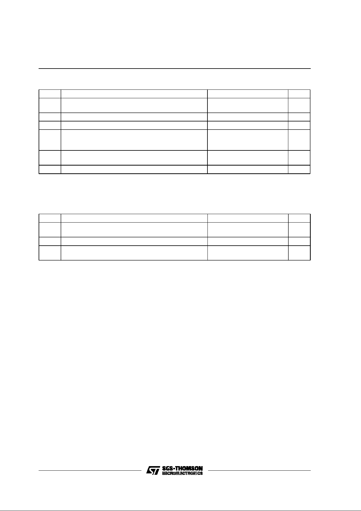
PIN CONNECTIONS
EY
(Plastic Package)F(Ceramic Frit Seal Package)
M1
(MicroPackage)C1(PlasticChip Carrier)
ORDER CODES :
HCC40XXBF HCF40XXBM1
HCF40XXBEY HCF40XXBC1
4011B 4012B 4023B
1/12
ABSOLUTE M AXI MU M RATI NGS
Symbol Parameter Val ue Unit
V
DD
* Supply Voltage : HCC Types
HCF Types
– 0.5 to + 20
– 0.5 to + 18
V
V
V
i
Input Voltage – 0.5 to VDD+ 0.5 V
I
I
DC Input Current (any one input) ± 10 mA
P
tot
Total Power Dissipation (per package)
Dissipation per Output Transistor
for Top= Full Package-temperature Range
200
100
mW
mW
T
op
Operating Temperature : HCC Types
HCF Types
–55to+125
–40to+85
°C
°C
T
stg
Storage Temperature – 65 to + 150 °C
RECOMMENDED OPERATING CONDITIONS
Symbol Pa ramet er Valu e Un i t
V
DD
Supply Voltage : HC C Types
HCF Types
3to18
3to15
V
V
V
I
Input Voltage 0 to V
DD
V
T
op
Operating Temperature : HCC Types
HCF Types
–55to+125
–40to+85
°C
°C
Stresses above those listed under ”Absolute Maximum Ratings” may cause permanent damage to the device. This is a stress rating only and
functionaloperationofthedeviceattheseoranyotherconditionsabove thoseindicatedintheoperationalsectionsofthisspecificationisnotimplied.
Exposure to absolute maximum rating conditions forexternal periodsmay affectdevice reliability.
* Allvoltage values are referred to VSSpinvoltage.
HCC/H FC4011B/12B/23B
2/12
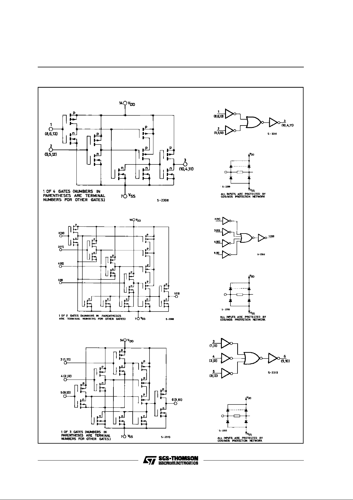
SCHEMATIC AND LOGIC DIAGRAMS
4011B
4023B
4012B
HCC/HCF4011B/12B/23B
3/12
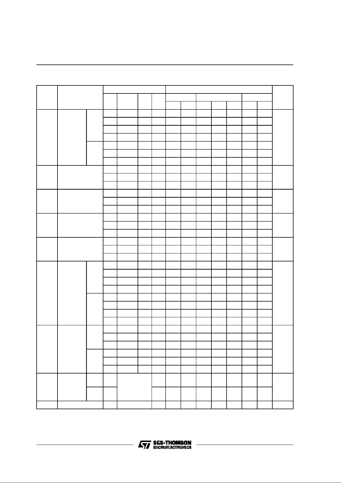
STATIC ELECTRICAL CHARACTERISTICS (over recommended operating conditions)
Test Conditions Valu e
V
I
V
O
|IO|V
DD
T
Low
* 25°CT
High
*
Symbol Parameter
(V) (V) (µA) (V)
Min. Max. Min. Typ. Max. Min. Max.
Unit
I
L
Quiescent
Current
HCC
Types
0/5 5 0.25 0.01 0.25 7.5
µA
0/10 10 0.5 0.01 0.5 15
0/15 15 1 0.01 1 30
0/20 20 5 0.02 5 150
HCF
Types
0/ 5 5 1 0.01 1 7.5
0/10 10 2 0.01 2 15
0/15 15 4 0.01 4 30
V
OH
Output High
Voltage
0/5 < 1 5 4.95 4.95 4.95
V
0/10 < 1 10 9.95 9.95 9.95
0/15 < 1 15 14.95 14.95 14.95
V
OL
Output Low
Voltage
5/0 < 1 5 0.05 0.05 0.05
V
10/0 < 1 10 0.05 0.05 0.05
15/0 < 1 15 0.05 0.05 0.05
V
IH
Input High
Voltage
0.5/4.5 < 1 5 3.5 3.5 3.5
V
1/9 < 1 10 7 7 7
1.5/13.5 < 1 15 11 11 11
V
IL
Input Low
Voltage
4.5/0.5 < 1 5 1.5 1.5 1.5
V
9/1 < 1 10 3 3 3
13.5/1.5 < 1 15 4 4 4
I
OH
Output
Drive
Current
HCC
Types
0/5 2.5 5 – 2 – 1.6 – 3.2 – 1.15
mA
0/5 4.6 5 – 0.64 – 0.51 – 1 – 0.36
0/10 9.5 10 – 1.6 – 1.3 – 2.6 – 0.9
0/15 13.5 15 – 4.2 – 3.4 – 6.8 – 2.4
HCF
Types
0/5 2.5 5 – 1.53 – 1.36 – 3.2 – 1.1
0/5 4.6 5 – 0.52 – 0.44 – 1 – 0.36
0/10 9.5 10 – 1.3 – 1.1 – 2.6 – 0.9
0/15 13.5 15 – 3.6 – 3.0 – 6.8 – 2.4
I
OL
Output
Sink
Current
HCC
Types
0/5 0.4 5 0.64 0.51 1 0.36
mA
0/10 0.5 10 1.6 1.3 2.6 0.9
0/15 1.5 15 4.2 3.4 6.8 2.4
HCF
Types
0/5 0.4 5 0.52 0.44 1 0.36
0/10 0.5 10 1.3 1.1 2.6 0.9
0/15 1.5 15 3.6 3.0 6.8 2.4
I
IH,IIL
Input
Leakage
Current
HCC
Types
0/18
Any Input
18 ± 0.1 ±10–5± 0.1 ± 1
µA
HCF
Types
0/15 15 ± 0.3 ±10
–5
± 0.3 ± 1
C
I
Input Capacitance Any Input 5 7.5 pF
*T
LOW
=–55°Cfor HCC device : – 40°CforHCF device.
*T
HIGH
=+ 125°C forHCC device : + 85°C for HCF device.
TheNoise Margin for both”1” and ”0” level is : 1V min.with VDD=5V, 2V min.with VDD= 10V,2.5V withVDD= 15V.
HCC/H FC4011B/12B/23B
4/12
 Loading...