


MCH6202
Any and all SANYO products described or contained herein do not have specifications that can handle
applications that require extremely high levels of reliability, such as life-support systems, aircraft’s
control systems, or other applications whose failure can be reasonably expected to result in serious
physical and/or material damage. Consult with your SANYO representative nearest you before using
any SANYO products described or contained herein in such applications.
SANYO assumes no responsibility for equipment failures that result from using products at values that
exceed, even momentarily, rated values (such as maximum ratings, operating condition ranges,or other
parameters) listed in products specifications of any and all SANYO products described or contained
herein.
PNP/NPN Epitaxial Planar Silicon Transistors
DC/DC Converter Applications
Ordering number:ENN6480
MCH6102/MCH6202
SANYO Electric Co.,Ltd. Semiconductor Company
TOKYO OFFICE Tokyo Bldg., 1-10, 1 Chome, Ueno, Taito-ku, TOKYO, 110-8534 JAPAN
83100TS (KOTO) TA-2843 No.6480–1/5
0.250.25
2.1
1.6
2.0
0.65
0.3
0.85
0.15
0.15
13
2
64
5
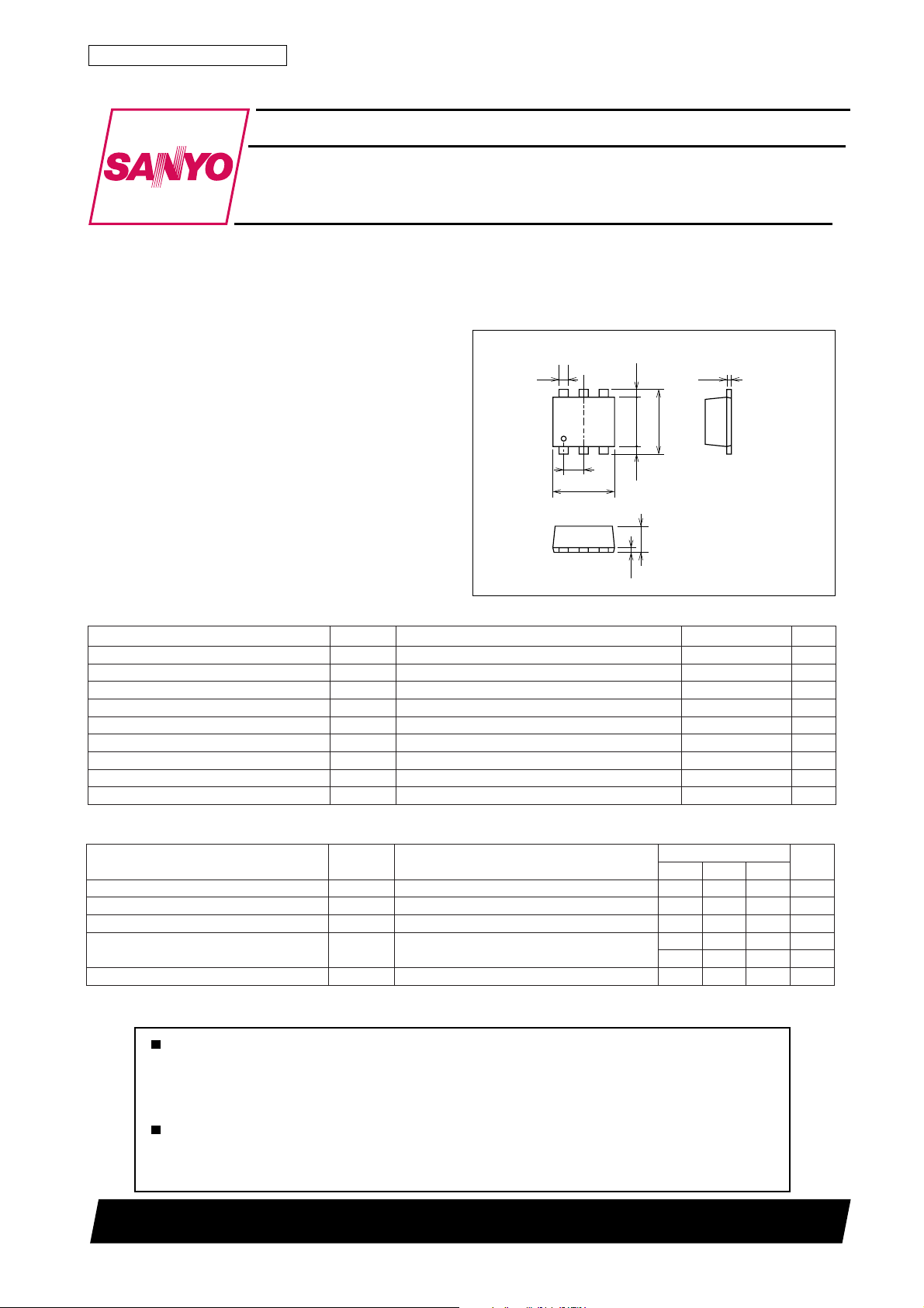
Package Dimensions
unit:mm
2177
[MCH6102/MCH6202]
Applications
· Relay drivers, lamp drivers, motor drivers.
Features
· Adoption of MBIT processes.
· Large current capacitance.
· Low collector-to-emitter saturation voltage.
· High-speed switching.
· Ultrasmall package facilitates miniaturization in end
products (mounting height : 0.85mm).
· High allowable power dissipation.
˚C
˚C
Electrical Characteristics at Ta = 25˚C
1 : Collector
2 : Collector
3 : Base
4 : Emitter
5 : Collector
6 : Collector
SANYO : MCPH6
Mounted on a ceramic board (600mm
2
×0.8mm)
Continued on next page.
Specifications
( ) : MCH6102
Absolute Maximum Ratings at Ta = 25˚C
retemaraPlobmySsnoitidnoCsgnitaRtinU
egatloVesaB-ot-rotcelloCV
OBC
04)03–(V
egatloVrettimE-ot-rotcelloCV
OEC
03)–(V
egatloVesaB-ot-rettimEV
OBE
5)–(V
tnerruCrotcelloCI
C
5.1)–(A
)esluP(tnerruCrotcelloCI
PC
3)–(A
tnerruCesaBI
B
003)–(Am
noitapissiDrotcelloCP
C
0.1W
erutarepmeTnoitcnuJjT 051
erutarepmeTegarotSgtsT 051+ot55–
retemaraPlobmySsnoitidnoC
sgnitaR
tinU
nimpytxam
tnerruCffotuCrotcelloCI
OBC
V
BC
I,V03)–(=
E
0=1.0)–(Aµ
tnerruCffotuCrettimEI
OBE
V
BE
I,V4)–(=
C
0=1.0)–(Aµ
niaGtnerruCCD
h
EF
V
EC
I,V2)–(=
C
Am001)–(=
002065
tcudorPhtdiwdnaB-niaGf
T
V
EC
I,V01)–(=
C
Am003)–(=
)054(zHM
005zHM
ecnaticapaCtuptuOboCV
BC
zHM1=f,V01)–(=
8)9(Fp
MCH6102/MCH6202
No.6480–2/5
Continued from preceding page.
Switching Time Test Circuit
retemaraPlobmySsnoitidnoC
sgnitaR
tinU
nimpytxam
egatloVnoitarutaSrettimE-ot-rotcelloCV
EC
)tas(I
C
I,Am057)–(=
B
Am51)–(=
)052–()573–(Vm
051522Vm
egatloVnoitarutaSrettimE-ot-esaBV
EB
)tas(I
C
I,Am057)–(=
B
Am51)–(=58.0)–(2.1)–(V
egatloVnwodkaerBesaB-ot-rotcelloCV
OBC)RB(
I
C
I,Aµ01)–(=
E
0=
)03–(V
04V
egatloVnwodkaerBrettimE-ot-rotcelloCV
OEC)RB(
I
C
R,Am1)–(=
EB
=∞ 03)–(V
egatloVnwodkaerBesaB-ot-rettimEV
OBE)RB(
I
E
I,Aµ01)–(=
C
0=5)–(V
emiTNO-nruTt
no
.tiucrictsetdeificepseeS
53)73(sn
emiTegarotSt
gts
.tiucrictsetdeificepseeS
)511(sn
502sn
emiTllaFt
f
.tiucrictsetdeificepseeS
23)62(sn
V
R
R
L
=16Ω
V
CC
=12VV
BE
= --5V
(For PNP, the polarity is reversed.)
20I
B1
= --20I
B2
= I
C
=750mA
+
+
50Ω
INPUT
OUTPUT
R
B
100µF 470µF
PW=20µs
I
B1
I
B2
D.C.≤1%
--2.0
--1.6
--1.2
--0.8
--0.4
0
0 --200 --400 --600 --800 --1000
I
C
-- V
CE
--4mA
--2mA
--6mA
--8mA
--10mA
--15mA
--20mA
--30mA
--40mA
--50mA
I
B
=0
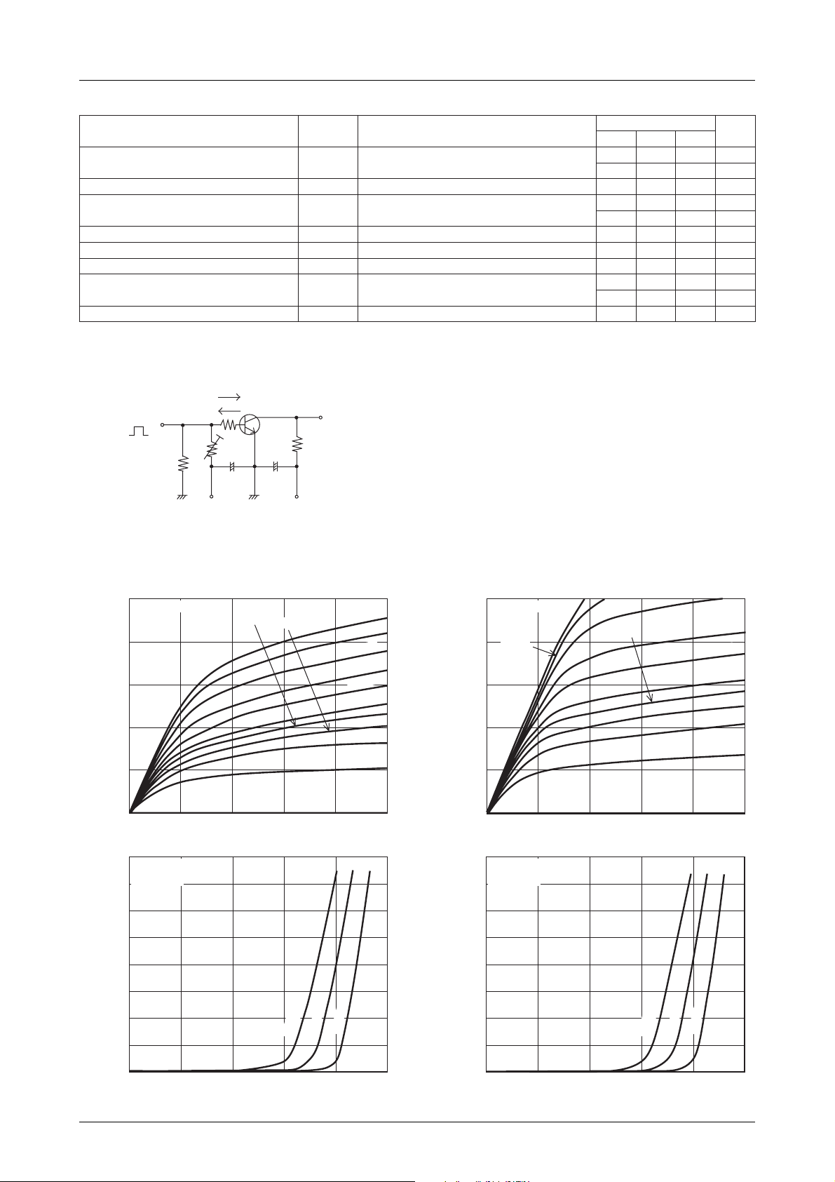
MCH6102
IT01872
--1.4
--1.6
--1.2
--1.0
--0.8
--0.6
--0.4
--0.2
0
0 --0.2 --0.4 --0.6 --0.8 --1.0
I
C
-- V
BE
IT01874
Ta=75
°C
25
°C
--25
°C
MCH6102
V
CE
= --2V
1.4
1.6
1.2
1.0
0.8
0.6
0.4
0.2
0
0 0.2 0.4 0.6 0.8 1.0
Ta=75°C
25
°C
--25
°C
MCH6202
V
CE
=2V
0.8
1.2
1.6
2.0
0.4
0
0 200 400 600 800 1000
I
C
-- V
CE
2mA
4mA
8mA
6mA
10mA
15mA
20mA
30mA
50mA
40mA
I
B
=0
IT01873
I
C
-- V
BE
IT01875
MCH6202
Collector Current, I
C
–A
Collector-to-Emitter Voltage, V
CE
–mV
Collector Current, I
C
–A
Base-to-Emitter Voltage, V
BE
–V
Collector Current, I
C
–A
Collector-to-Emitter Voltage, V
CE
–mV
Collector Current, I
C
–A
Base-to-Emitter Voltage, V
BE
–V
 Loading...