


Samsung K4D263238E-GC40, K4D263238E-GC36, K4D263238E-GC33, K4D263238E-GC2A, K4D263238E-GC25 Datasheet
...K4D263238E-GC |
128M GDDR SDRAM |
128Mbit GDDR SDRAM
1M x 32Bit x 4 Banks
Graphic Double Data Rate
Synchronous DRAM
with Bi-directional Data Strobe and DLL (144-Ball FBGA)
Revision 1.7
November 2003
Samsung Electronics reserves the right to change products or specification without notice.
- 1 - |
Rev 1.7 (Nov. 2003) |
|
|
|
|

K4D263238E-GC |
128M GDDR SDRAM |
Revision History
Revision 1.7 (November 14, 2003)
• Typo corrected
Revision 1.6 (August 14, 2003)
• Added a note for the input reference voltage of clock in case of differential clocks
Revision 1.5 (August 11, 2003)
• Typo corrected
Revision 1.4 (April 30, 2003)
• Added Lead free package part number in the datasheet
Revision 1.3 (April 14, 2003)
• K4D263238E-GC2A/33/36 support wide voltage range from 2.375V to 2.94V
Revision 1.2 (April 7, 2003)
• Removed K4D263238E-GL36 from the spec.
Revision 1.1 (March 17, 2003)
• Typo corrected
Revision 1.0 (February 13, 2003)
•Defined DC spec
•Added K4D263238E-GC25 and K4D263238E-GL36 in the spec.
- 2 - |
Rev 1.7 (Nov. 2003) |
|
|
|
|
K4D263238E-GC |
128M GDDR SDRAM |
1M x 32Bit x 4 Banks Graphic Double Data Rate Synchronous DRAM with Bi-directional Data Strobe and DLL
FEATURES
•VDD/VDDQ = 2.8V ± 5% for -GC25
•VDD/VDDQ = 2.5V ± 5% for -GC2A/33/36/40/45
•SSTL_2 compatible inputs/outputs
•4 banks operation
•MRS cycle with address key programs
-. Read latency 3, 4, 5 (clock)
-. Burst length (2, 4, 8 and Full page) -. Burst type (sequential & interleave)
•Full page burst length for sequential burst type only
•Start address of the full page burst should be even
•All inputs except data & DM are sampled at the positive going edge of the system clock
•Differential clock input
•No Wrtie-Interrupted by Read Function
•4 DQS’s ( 1DQS / Byte )
•Data I/O transactions on both edges of Data strobe
•DLL aligns DQ and DQS transitions with Clock transition
•Edge aligned data & data strobe output
•Center aligned data & data strobe input
•DM for write masking only
•Auto & Self refresh
•32ms refresh period (4K cycle)
•144-Ball FBGA
•Maximum clock frequency up to 400MHz
•Maximum data rate up to 800Mbps/pin
ORDERING INFORMATION
Part NO. |
Max Freq. |
Max Data Rate |
Interface |
Package |
K4D263238E-GC25 |
400MHz |
800Mbps/pin |
SSTL_2 |
|
(VDD/VDDQ=2.8V) |
|
|||
|
|
|
|
|
|
|
|
|
|
K4D263238E-GC2A |
350MHz |
700Mbps/pin |
|
|
|
|
|
|
|
K4D263238E-GC33 |
300MHz |
600Mbps/pin |
SSTL_2 |
144-Ball FBGA |
K4D263238E-GC36 |
275MHz |
550Mbps/pin |
|
|
(VDD/VDDQ=2.5V) |
|
|||
|
|
|
|
|
K4D263238E-GC40 |
250MHz |
500Mbps/pin |
|
|
|
|
|||
|
|
|
|
|
K4D263238E-GC45 |
222MHz |
444Mbps/pin |
|
|
|
|
|
|
|
K4D263238E-VC is the Lead Free package part number.
GENERAL DESCRIPTION
FOR 1M x 32Bit x 4 Bank DDR SDRAM
The K4D263238E is 134,217,728 bits of hyper synchronous data rate Dynamic RAM organized as 4 x1,048,576 words by 32 bits, fabricated with SAMSUNG’s high performance CMOS technology. Synchronous features with Data Strobe allow extremely high performance up to 3.2GB/s/chip. I/O transactions are possible on both edges of the clock cycle. Range of operating frequencies, programmable burst length and programmable latencies allow the device to be useful for a variety of high performance memory system applications.
- 3 - |
Rev 1.7 (Nov. 2003) |
|
|
|
|

K4D263238E-GC |
128M GDDR SDRAM |
PIN CONFIGURATION (Top View)
|
2 |
3 |
4 |
5 |
6 |
7 |
8 |
9 |
10 |
11 |
12 |
13 |
B |
DQS0 |
DM0 |
VSSQ |
DQ3 |
DQ2 |
DQ0 |
DQ31 |
DQ29 |
DQ28 |
VSSQ |
DM3 |
DQS3 |
C |
DQ4 |
VDDQ |
NC |
VDDQ |
DQ1 |
VDDQ |
VDDQ |
DQ30 |
VDDQ |
NC |
VDDQ |
DQ27 |
D |
DQ6 |
DQ5 |
VSSQ |
VSSQ |
VSSQ |
VDD |
VDD |
VSSQ |
VSSQ |
VSSQ |
DQ26 |
DQ25 |
E |
DQ7 |
VDDQ |
VDD |
VSS |
VSSQ |
VSS |
VSS |
VSSQ |
VSS |
VDD |
VDDQ |
DQ24 |
F |
DQ17 |
DQ16 |
VDDQ |
VSSQ |
VSS |
VSS |
VSS |
VSS |
VSSQ |
VDDQ |
DQ15 |
DQ14 |
Thermal |
Thermal |
Thermal |
Thermal |
|||||||||
G |
DQ19 |
DQ18 |
VDDQ |
VSSQ |
VSS |
VSS |
VSS |
VSS |
VSSQ |
VDDQ |
DQ13 |
DQ12 |
Thermal |
Thermal |
Thermal |
Thermal |
|||||||||
H |
DQS2 |
DM2 |
NC |
VSSQ |
VSS |
VSS |
VSS |
VSS |
VSSQ |
NC |
DM1 |
DQS1 |
Thermal |
Thermal |
Thermal |
Thermal |
|||||||||
J |
DQ21 |
DQ20 |
VDDQ |
VSSQ |
VSS |
VSS |
VSS |
VSS |
VSSQ |
VDDQ |
DQ11 |
DQ10 |
Thermal |
Thermal |
Thermal |
Thermal |
|||||||||
K |
DQ22 |
DQ23 |
VDDQ |
VSSQ |
VSS |
VSS |
VSS |
VSS |
VSSQ |
VDDQ |
DQ9 |
DQ8 |
L |
CAS |
WE |
VDD |
VSS |
A10 |
VDD |
VDD |
RFU1 |
VSS |
VDD |
NC |
NC |
M |
RAS |
NC |
NC |
BA1 |
A2 |
A11 |
A9 |
A5 |
RFU2 |
CK |
CK |
MCL |
N |
CS |
NC |
BA0 |
A0 |
A1 |
A3 |
A4 |
A6 |
A7 |
A8/AP |
CKE |
VREF |
NOTE:
1.RFU1 is reserved for A12
2.RFU2 is reserved for BA2
3.VSS Thermal balls are optional
PIN DESCRIPTION
|
|
|
|
|
|
|
|
|
|
|
CK,CK |
|
Differential Clock Input |
|
BA0, BA1 |
Bank Select Address |
|||
|
CKE |
|
Clock Enable |
|
A0 ~A11 |
Address Input |
|||
|
|
|
|
|
|
|
|
|
|
|
|
|
|
|
Chip Select |
|
DQ0 ~ DQ31 |
Data Input/Output |
|
|
CS |
||||||||
|
|
|
|
|
|
Row Address Strobe |
|
VDD |
Power |
|
RAS |
||||||||
|
|
|
|
|
|
Column Address Strobe |
|
VSS |
Ground |
|
CAS |
||||||||
|
WE |
|
Write Enable |
|
VDDQ |
Power for DQ’s |
|||
|
|
|
|
|
|
|
|||
|
DQS |
|
Data Strobe |
|
VSSQ |
Ground for DQ’s |
|||
|
|
|
|
|
|
|
|||
|
DM |
|
Data Mask |
|
NC |
No Connection |
|||
|
|
|
|
|
|
|
|||
|
RFU |
|
Reserved for Future Use |
|
MCL |
Must Connect Low |
|||
|
|
|
|
|
|
|
|
|
|
- 4 - Rev 1.7 (Nov. 2003)
K4D263238E-GC |
|
|
|
|
|
|
|
128M GDDR SDRAM |
|||||||||||||
INPUT/OUTPUT FUNCTIONAL DESCRIPTION |
|||||||||||||||||||||
|
|
|
|
|
|
|
|
|
|
|
|
|
|
|
|
|
|
|
|
|
|
|
|
|
Symbol |
Type |
|
|
|
|
|
|
Function |
||||||||||
|
|
|
|
|
|
|
|
|
|
|
The differential system clock Input. |
||||||||||
CK, |
CK*1 |
Input |
|
All of the inputs are sampled on the rising edge of the clock except |
|||||||||||||||||
|
|
|
|
|
|
|
|
|
|
|
DQ’s and DM’s that are sampled on both edges of the DQS. |
||||||||||
|
|
|
|
|
|
|
|
|
|
|
|
|
|
|
|
||||||
|
|
|
|
|
|
|
|
|
|
|
Activates the CK signal when high and deactivates the |
|
signal |
||||||||
|
|
|
|
|
|
|
|
|
|
CK |
|||||||||||
|
CKE |
Input |
|
when low. By deactivating the clock, CKE low indicates the Power |
|||||||||||||||||
|
|
|
|
|
|
|
|
|
|
|
down mode or Self refresh mode. |
||||||||||
|
|
|
|
|
|
|
|
|
|
|
|
|
|
|
|||||||
|
|
|
|
|
|
|
|
|
|
|
|
enables the command decoder when low and disabled the com- |
|||||||||
|
|
|
|
|
|
|
|
|
|
|
CS |
||||||||||
|
|
|
CS |
|
|
|
Input |
|
mand decoder when high. When the command decoder is disabled, |
||||||||||||
|
|
|
|
|
|
|
|
|
|
|
new commands are ignored but previous operations continue. |
||||||||||
|
|
|
|
|
|
|
|
|
|
|
|
|
|
||||||||
|
|
|
|
|
|
|
|
|
Input |
|
Latches row addresses on the positive going edge of the CK with |
||||||||||
|
RAS |
|
|||||||||||||||||||
|
|
|
|
|
|
|
|
|
|
|
|
|
|||||||||
|
|
RAS low. Enables row access & precharge. |
|||||||||||||||||||
|
|
|
|
|
|
|
|
|
|
|
|||||||||||
|
|
|
|
|
|
|
|
|
|
|
Latches column addresses on the positive going edge of the CK with |
||||||||||
|
CAS |
Input |
|
||||||||||||||||||
|
|
|
|
|
|
|
|
|
|
|
|
|
|||||||||
|
|
CAS low. Enables column access. |
|||||||||||||||||||
|
|
|
|
|
|
|
|
|
|
|
|||||||||||
|
|
|
|
|
|
|
|
|
|
|
Enables write operation and row precharge. |
||||||||||
|
|
WE |
Input |
|
|||||||||||||||||
|
|
|
|
|
|
|
|
|
|
|
|
|
|
||||||||
|
|
|
Latches data in starting from CAS, WE active. |
||||||||||||||||||
|
|
|
|
|
|
|
|
|
|
|
|||||||||||
|
|
|
|
|
|
|
|
|
|
|
Data input and output are synchronized with both edge of DQS. |
||||||||||
DQS0 ~ DQS3 |
Input/Output |
|
DQS0 for DQ0 ~ DQ7, DQS1 for DQ8 ~ DQ15, DQS2 for DQ16 ~ DQ23, |
||||||||||||||||||
|
|
|
|
|
|
|
|
|
|
|
DQS3 for DQ24 ~ DQ31. |
||||||||||
|
|
|
|
|
|
|
|
|
|
|
|
|
|
||||||||
|
|
|
|
|
|
|
|
|
|
|
Data In mask. Data In is masked by DM Latency=0 when DM is high |
||||||||||
DM0 ~ DM3 |
Input |
|
in burst write. DM0 for DQ0 ~ DQ7, DM1 for DQ8 ~ DQ15, DM2 for |
||||||||||||||||||
|
|
|
|
|
|
|
|
|
|
|
DQ16 ~ DQ23, DM3 for DQ24 ~ DQ31. |
||||||||||
|
|
|
|
|
|||||||||||||||||
DQ0 ~ DQ31 |
Input/Output |
Data inputs/Outputs are multiplexed on the same pins. |
|||||||||||||||||||
|
|
|
|
|
|||||||||||||||||
BA0, BA1 |
Input |
Selects which bank is to be active. |
|||||||||||||||||||
|
|
|
|
|
|
|
|
|
|
|
|
|
|
||||||||
|
|
|
|
|
|
|
|
|
|
|
Row/Column addresses are multiplexed on the same pins. |
||||||||||
A0 ~ A11 |
Input |
|
Row addresses : RA0 ~ RA11, Column addresses : CA0 ~ CA7. |
||||||||||||||||||
|
|
|
|
|
|
|
|
|
|
|
Column address CA8 is used for auto precharge. |
||||||||||
|
|
|
|
|
|||||||||||||||||
VDD/VSS |
Power Supply |
Power and ground for the input buffers and core logic. |
|||||||||||||||||||
|
|
|
|
|
|
|
|
|
|
|
|
|
|
||||||||
VDDQ/VSSQ |
Power Supply |
|
Isolated power supply and ground for the output buffers to provide |
||||||||||||||||||
|
improved noise immunity. |
||||||||||||||||||||
|
|
|
|
|
|
|
|
|
|
|
|||||||||||
|
|
|
|
|
|||||||||||||||||
VREF |
Power Supply |
Reference voltage for inputs, used for SSTL interface. |
|||||||||||||||||||
|
|
|
|
|
|
||||||||||||||||
NC/RFU |
No connection/ |
|
This pin is recommended to be left "No connection" on the device |
||||||||||||||||||
|
|
|
|
|
|
|
|
|
Reserved for future use |
|
|
|
|
|
|
|
|
|
|
|
|
|
|
|
|
|
|
||||||||||||||||
MCL |
Must Connect Low |
|
Must connect low |
||||||||||||||||||
|
|
|
|
|
|
|
|
|
|
|
|
|
|
|
|
|
|
|
|
|
|
|
|
|
|
|
|
|
|
|
|
|
|
|
|
|
|
|
|
|
|
|
|
*1 : The timing reference point for the differential clocking is the cross point of CK and CK.
For any applications using the single ended clocking, apply VREF to CK pin.
- 5 - |
Rev 1.7 (Nov. 2003) |
|
|
|
|
K4D263238E-GC |
128M GDDR SDRAM |
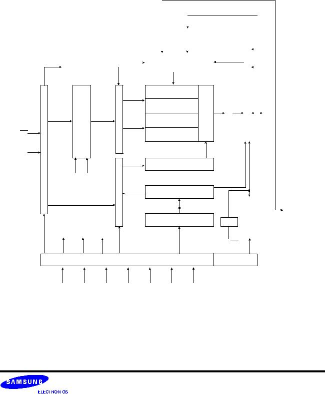
BLOCK DIAGRAM (1Mbit x 32I/O x 4 Bank)
|
|
|
|
|
|
|
|
32 |
|
|
|
|
|
|
|
|
|
|
|
|
|
||
|
|
|
|
|
|
|
|
|
|
|
|
|
|
|
|
|
|
|
|
|
Intput Buffer |
|
|
|
CK, |
|
|
|
|
|
|
|
|
|
|
|
|
|
|
|
|
|
|
|
|
||
|
CK |
|
Data Input Register |
||||||||
Bank Select |
|
|
|
|
|
|
Serial to parallel |
||||
|
|
|
|
|
|
||||||
|
|
|
|
|
|
|
|
|
|
|
|
64
|
Address |
BufferRow |
CounterRefresh |
DecoderRow |
|
1Mx32 |
AMPSense |
|
|
1Mx32 |
|||||
|
|
|
|
|
|
|
|
|
|
|
|
|
|
1Mx32 |
|
CK,CK |
Register |
|
|
|
|
1Mx32 |
|
ADDR |
|
|
|
|
Column Decoder |
|
|
|
|
|
|
|
|
|
|
|
|
LRAS |
LCBR |
Buffer.Col |
|
Latency & Burst Length |
|
|
|
|
|
|
|
||
|
LCKE |
|
|
|
|
Programming Register |
|
|
LCBR |
LWE |
|
|
|
||
|
LRAS |
|
|
|
|||
|
|
|
|
LCAS |
LWCBR |
|
|
|
|
|
|
|
|
|
|
|
|
|
|
|
Timing Register |
|
|
64 |
bit-2 |
32 |
|
prefetch |
|||
|
|
||
|
|
|
DLL
CK,CK
|
|
|
|
|
|
I/O |
|
|
LWE |
||
Control |
|
|
|
|
|
|
|
LDMi |
|||
|
|
|
|
|
|
|
|
|
|
|
|
|
|
|
|
|
|
Output |
|
|
|
x32 |
|
Buffer |
|
|
|
||
|
|
|
|||
|
DQi |
||||
|
|
||||
|
|
|
|
|
|
Strobe .Gen |
|
(DQS0~DQS3) |
|
|
Data Strobe |
|
|
|
|
|
|
LDMi
|
|
|
|
|
|
|
|
|
|
|
CK,CK CKE |
CS |
|
RAS CAS |
|
WE |
DMi |
||||
- 6 - |
Rev 1.7 (Nov. 2003) |
|
|
|
|
 Loading...