

Samsung RE23EO, RE40EO, LE23R51B, RE32EO, LE26R51B Service Manual
...
TFT-LCD TV/MONITOR
Chassis Model
RE23EO LE23R51B
RE26EO LE26R51B
RE32EO LE32R51B
RE40EO LE40R51B
Manual
SERVICE
TFT-LCD TV/MONITOR CONTENTS
1. Precautions
2. Product Specifications
3. Disassembly & Reassembly
4. Alignment & Adjustments
5. Troubleshooting
6. Exploded View & Parts List
7. Parts List
8. Block Diagram
9. Wiring Diagram
10. PCB Layout
11. Schematic Diagrams
12. Panel Description
Samsung Electronics Co.,Ltd.
416, Maetan-3Dong, Yeongtong-Gu, Suwon City, Gyeonggi-Do,
Korea, 443-742
Printed in Korea
P/N : BN82-00128A-00
URL : http://itself.sec.samsung.co.kr/
h This Service Manual is a property of
Samsung Electronics Co., Ltd.
Any unauthorized use of Manual can be
punished under applicable International
and/or domestic law.
1 Precautions
1-1
1-1-1 Warnings
1. For continued safety, do not attempt to modify the circuit
board.
2. Disconnect the AC power and DC Power Jack before
servicing.
1-1-2 Servicing the LCD Monitor
1. When servicing the LCD Monitor Disconnect the AC
line cord from the AC outlet.
2. It is essential that service technicians have an accurate
voltage meter available at all times. Check the
calibration of this meter periodically.
1-1-3 Fire and Shock Hazard
Before returning the monitor to the user, perform the
following safety checks:
1. Inspect each lead dress to make certain that the leads are
not pinched or that hardware is not lodged between the
chassis and other metal parts in the monitor.
2. Inspect all protective devices such as nonmetallic control
knobs, insulating materials, cabinet backs, adjustment
and compartment covers or shields, isolation resistorcapacitor networks, mechanical insulators, etc.
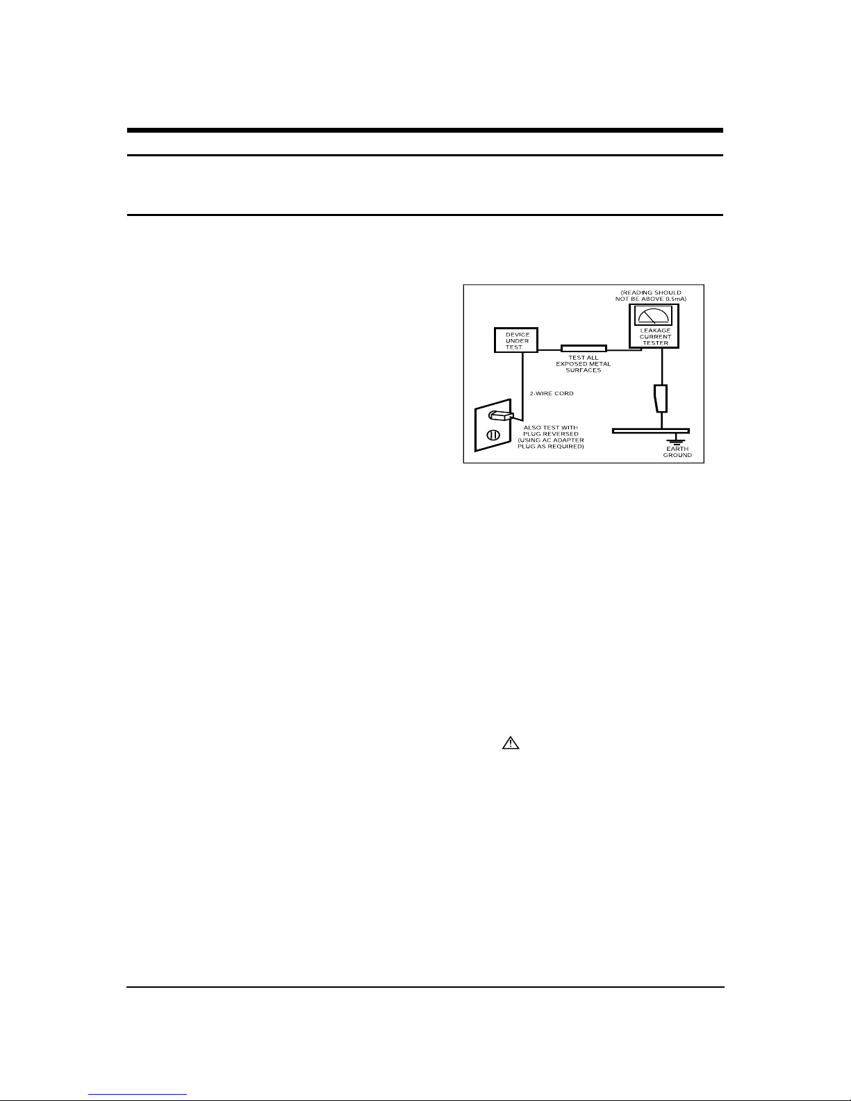
3. Leakage Current Hot Check (Figure 1-1):
WARNING: Do not use an isolation
transformer during
this test.
Use a leakage current tester or a metering system that
complies with American National Standards Institute
(ANSI C101.1, Leakage Current for Appliances), and
Underwriters Laboratories (UL Publication UL1410,
59.7).
Figure 1-1. Leakage Current Test Circuit
4. With the unit completely reassembled, plug the AC line
cord directly into a 120V AC outlet. With the units AC
switch first in the ON position and then OFF, measure
the current between a known earth ground (metal water
pipe, conduit, etc.) and all exposed metal parts,
including: metal cabinets, screwheads and control shafts.
The current measured should not exceed 0.5 milliamp.
Reverse the power-plug prongs in the AC outlet and
repeat the test.
1-1-4 Product Safety Notices
Some electrical and mechanical parts have special safetyrelated characteristics which are often not evident from visual
inspection. The protection they give may not be obtained by
replacing them with components rated for higher voltage,
wattage, etc. Parts that have special safety characteristics are
identified by on schematics and parts lists. A substitute
replacement that does not have the same safety characteristics
as the recommended replacement part might create shock, fire
and/or other hazards. Product safety is under review
continuously and new instructions are issued whenever
appropriate.
1 Precautions
Follow these safety, servicing and ESD precautions to prevent damage and to protect against potential hazards such as electrical shock.
1-1 Safety Precautions

1 Precautions
1-2
1-2-1 General Ser vicing
Precautions
1. Always unplug the units AC power cord from the AC
power source and disconnect the DC Power Jack before
attempting to:
(a) remove or reinstall any component or assembly, (b)
disconnect PCB plugs or connectors, (c) connect a test
component in parallel with an electrolytic capacitor.
2. Some components are raised above the printed circuit
board for safety. An insulation tube or tape is sometimes
used. The internal wiring is sometimes clamped to
prevent contact with thermally hot components. Reinstall
all such elements to their original position.
3. After servicing, always check that the screws,
components and wiring have been correctly reinstalled.
Make sure that the area around the serviced part has not
been damaged.
1. Immediately before handling any semiconductor
components or assemblies, drain the electrostatic charge
from your body by touching a known earth ground.
Alternatively, wear a discharging wrist-strap device. To
avoid a shock hazard, be sure to remove the wrist strap
before applying power to the monitor.
2. After removing an ESD-equipped assembly, place it on a
conductive surface such as aluminum foil to prevent
accumulation of an electrostatic charge.
3. Do not use freon-propelled chemicals. These can
generate electrical charges sufficient to damage ESDs.
4. Use only a grounded-tip soldering iron to solder or
desolder ESDs.
5. Use only an anti-static solder removal device. Some
solder removal devices not classified as anti-static can
generate electrical charges sufficient to damage ESDs.
4. Check the insulation between the blades of the AC plug
and accessible conductive parts (examples: metal panels,
input terminals and earphone jacks).
5. Insulation Checking Procedure: Disconnect the power
cord from the AC source and turn the power switch ON.
Connect an insulation resistance meter (500 V) to the
blades of the AC plug.
The insulation resistance between each blade of the AC
plug and accessible conductive parts (see above) should
be greater than 1 megohm.
6. Always connect a test instruments ground lead to the
instrument chassis ground before connecting the positive
lead; always remove the instruments ground lead last.
6. Do not remove a replacement ESD from its protective
package until you are ready to install it. Most
replacement ESDs are packaged with leads that are
electrically shorted together by conductive foam,
aluminum foil or other conductive materials.
7. Immediately before removing the protective material
from the leads of a replacement ESD, touch the
protective material to the chassis or circuit assembly into
which the device will be installed.
Caution:Be sure no power is applied to the
chassis or circuit and observe all
other safety precautions.
8. Minimize body motions when handling unpackaged
replacement ESDs. Motions such as brushing clothes
together, or lifting your foot from a carpeted floor can
generate enough static electricity to damage an ESD.
1-3 Electrostatically Sensitive Devices (ESD) Precautions
Some semiconductor (solid state) devices can be easily damaged by static electricity. Such components are commonly called
Electrostatically Sensitive Devices (ESD). Examples of typical ESD are integrated circuits and some field-effect transistors. The
following techniques will reduce the incidence of component damage caused by static electricity.
1-2 Ser vicing Precautions
WARNING: An electrolytic capacitor installed with the wrong polarity might explode.
Caution: Before servicing units covered by this service manual, read and follow the Safety Precautions
section of this manual.
Note: If unforeseen circumstances create conflict between the following servicing precautions and any of the safety
precautions, always follow the safety precautions.

4 Alignments and Adjustments
4-1
4 Alignments and Adjustments
4-1 General Alignment Instuction
1. Usually, a color TV-VCR needs only slight touch-up adjustment upon installation.
Check the basic characteristics such as height, horizontal and vertical sync.
2. Use the specified test equipment or its equivalent.
3. Correct impedance matching is essential.
4. Avoid overload. Excessive signal from a sweep generator might overload the front-end
of the TV. When inserting signal markers, do not allow the marker generator to distort
test result.
5. Connect the TV only to an AC power source with voltage and frequency as specified on
the backcover nameplate.
6. Do not attempt to connect or disconnect any wire while the TV is turned on. Make sure
that the power cord is disconnected before replacing any parts.
7. To protect aganist shock hazard, use an isolation transform.
4 Alignments and Adjustments
4-2
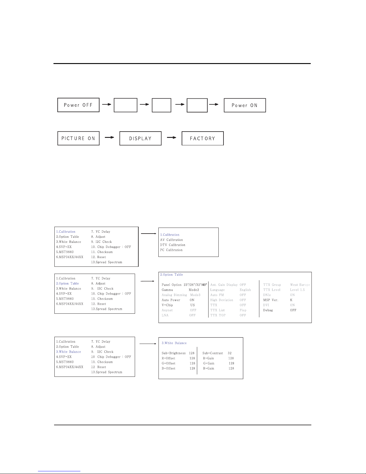
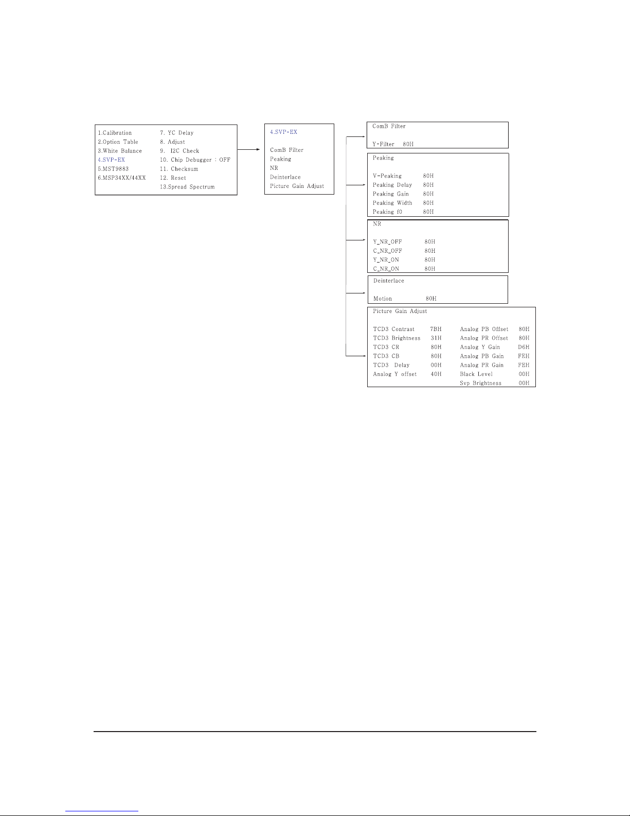
4-2-2 Factory Mode Tree
4-2 Factory Mode Adjustments
4-2-1 Entering Factory Mode
1. To enter “Service Mode” Press the remote -control keys in this sequence :
- If you do not have Factory remote - control
- If you have Factory remote - control
MENU MU TE
INFO
- The buttons are active in the service mode.
1. Remote - Control Key : Power, Arrow Up, Arrow Down, Arrow Left
Arrow Right, Menu, Enter, Number Key(0~9)
2. Function - Control Key : Power, CH +, CH -, VOL +, VOL -,
Menu, TV/VIDEO(Enter)
* Please set up for an appropriate INCH.
4 Alignments and Adjustments
4-3

4 Alignments and Adjustments
4-4
4 Alignments and Adjustments
4-5
4 Alignments and Adjustments
4-6
4 Alignments and Adjustments
4-7
4-3-1 White Balance - Calibration
4-3-2 White Balance - Adjustment
4 Alignments and Adjustments
4-8
4-3-3 Conditions for Measurement
1. On the basis of toshiba ABL pattern : High Light level (57 IRE)
- INPUT SIGNAL GENERATOR : MSPG-925LTH
* Mode NO 1 : 744X484@60 Hz
NO 6 : 1280X720@60 Hz
NO 21 : 1024X768@60 Hz
* Pattern NO 36 : 16 Color Pattern
NO 16 : Toshiba ABL Pattern
2. Optical measuring device : CA210 (FL)
Please use the MSPG-925 LTH generator for model LT26A33W.
4-3-4 Method of Adjustment
1. Adjust the basic level of DTV and PC input signals.
a) Set the input to the mode in which the adjustment will be made (DTV PC ).
* Input signal - DTV Mode : Model #6 (1280*720 Mode), Pattern #36
- PC Mode : Model #21 (1024*768 Mode), Pattern #16 (Picture 4-1)
b) Enter factory Calibration, confirm the ADC data (DTV, PC Mode Only).
* ADC default value : Table 4-3.
2. Adjust the white balance of RF, DTV, PC and DVI Modes.
a) Set the input to the mode in which the adjustment will be made(RF DTV PC DVI).
* Input signal - VIDEO Mode : Model #1 (744*484 Mode), Pattern #16
- DTV,DVI Mode : Model #6 (1280*720 Mode), Pattern #16
- PC Mode : Model #21 (1024*768 Mode), Pattern #16
b) Enter factory color control, confirm the data.
Picture 4-1 Toshiba ABL Pattern
4 Alignments and Adjustments
4-9
c) Adjust the low light. (Refer to table 1, 2 in adjustment position by mode)
- Adjust sub - Brightness to set the 'Y' value.
- Adjust red offset ('x') and blue offset ('y') to the color coordinates.
* Do not adjust green offset data.
d) Adjust the high light. (Refer to table 1, 2 in adjustment position by mode)
- Adjust red gain ('x') and blue gain ('y') to the color coordinates.
* Do not adjust the green gain and sub-contrast (Y) data.
Picture 4-2 Toshiba ABL Pattern
Picture 4-3 Toshiba ABL Pattern
Low light
Measurement point
High light
Measurement point
4 Alignments and Adjustments
4-10
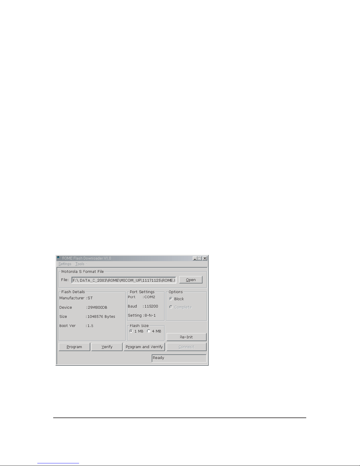
4-4 Flash ROM Update
1. Installthe Flash Downloader
ConnectSet(Service Jack)and Jig Cable to execute Program Update.
2. Flash Downloader program update
-Before Turning on the set,Click "connect"which is under of OSD Screen!
-Turn on the Set.
3.Open the New Update File and Click the Program and Verify.
4.Program update sledding ismarked sequently on OSD screen.
5.Afterprogram update completion,message should be pop up.
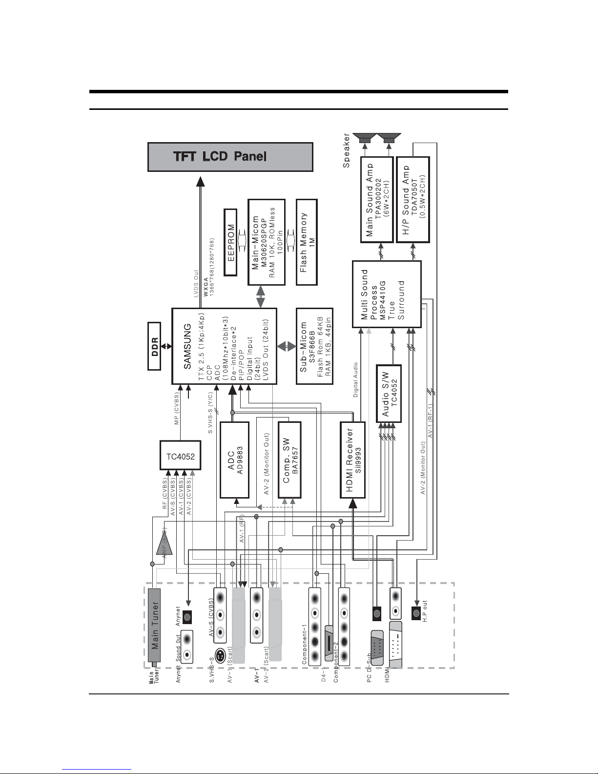
8 Block Diagrams
8-1
8 Block Diagram
-This Document can not be used without Samsung’s authorization.

8 Block Diagrams
8-2
Memo
3 Disassembly and Reassembly
3-1
3 Disassembly and Reassembly
This section of the service manual describes the disassembly and reassembly procedures for the LE23A41B/LE26A41B/LE32A41B LCD TV.
WARNING: This monitor contains electrostatically sensitive devices. Use caution when
handling these components.
3-1 LE23R51B Disassembly
Cautions: 1. Disconnect the monitor from the power source before disassembly.
2. Remove the stand and lift up the rear cover.
3. Remove 3 screws and lift up the jack cover.
Disconnect speaker cable, function cable from the
board.
4. Remove 9 screws from the boards.
5. Lift up the Power board and Main board.
1. Place LCD TV face down on cushioned table.
Remove 9 screws from the rear cover.
Remove 4 screws from grip on the stand. and
remove the stand.

3 Disassembly and Reassembly
3-2
3-2 LE26R51B, LE32R51B Disassembly
2. Remove 3 screws from the Jack cover.
Remove 12 screws from The board.
1. Place LCD TV face down on cushioned table.
Remove 14 screws from the rear cover.
Lift up the rear cover.
7. Lift up the shield cover and LCD panel.
6. Remove 9 screws and Lift up the shield panel and
remove 4 screws.
3 Disassembly and Reassembly
3-3
3-3 LE40R51B Disassembly
6. Lift up the BRKT.
2. Remove the stand and lift up the rear cover
1. Remove 8 screws from rearcover.
Remove 4 screws from grip on the stand.
4. Remove 11 screws from the shield.and lift up the
shield.
5. Remove 5 screws(Left :2/Right :3)
3 Disassembly and Reassembly
3-4
6. Remove 4 screws from the power board.
Disconnect Cables.
5. Remove 4screws from the Main board and lift up
the board.
3. Disconnect speaker cable, function cable and
Remove screws from the shield.
4. Disconnect Power Cables, LVDS Cable from
the power board.
3 Disassembly and Reassembly
3-5
10. Lift up the panel, Remove screws from the panel
BRKT(R/L).
Disconnect BRKT from the panel.
7. Disconnect inverter cable.
Lift up the power board.
9. Remove screws from the panel BRKT. Remove
screws from the cabinet BRKT and lift up the
panel Assy.
8. Remove screws.

3 Disassembly and Reassembly
3-6
3-4 Reassembly
Reassembly procedures are in the reverse order of dissasembly procedures.
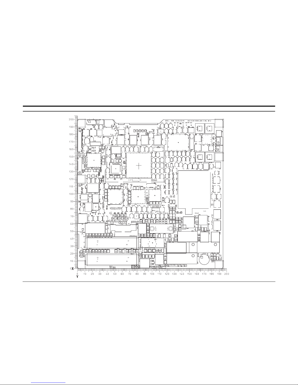
10 PCB Layout
10-1
10 PCB Layout
10 PCB Layout
10-2
D101 DIODE-SWITCHING 175.2 138.4
D102 DIODE-ZENER 166.0 118.4
D210 DIODE-ZENER 99.0 130.8
D211 DIODE-ZENER 100.2 146.6
D212 DIODE-ZENER 105.8 145.6
D213 DIODE-ZENER 104.2 130.8
D214 DIODE-ZENER 109.4 130.8
D215 DIODE-ZENER 108.8 145.6
D216 DIODE-ZENER 102.4 123.2
D217 DIODE-ZENER 107.6 122.8
D617 DIODE-ZENER 138.4 191.6
D620 DIODE-ZENER 160.0 172.8
D621 DIODE-ZENER 144.0 187.0
D622 DIODE-ARRAY 144.0 191.6
D701_EU DIODE-ZENER 13.2 23.2
D702 DIODE-ZENER 29.2 23.2
D703_EU DIODE-ZENER 21.2 23.2
D704 DIODE-ZENER 37.2 23.2
D705_EU DIODE-ZENER 9.2 23.2
D706 DIODE-ZENER 25.2 23.2
D707_EU DIODE-ZENER 17.2 23.2
D708 DIODE-ZENER 33.2 23.2
D709_EU DIODE-SWITCHING 85.2 63.2
D710_EU DIODE-SWITCHING 92.4 63.2
D7102 DIODE-SWITCHING 76.0 45.6
D7103 DIODE-SWITCHING 76.0 50.0
D7104 DIODE-SWITCHING 133.2 66.8
D7105 DIODE-SWITCHING 133.2 62.4
D7108 DIODE-ZENER 46.0 50.4
D7109 DIODE-ZENER 46.0 56.0
D711_EU DIODE-SWITCHING 99.6 63.2
D7110 DIODE-ZENER 42.0 50.4
D7111 DIODE-ZENER 42.0 56.0
D7112 DIODE-ZENER 160.0 61.6
D7113 DIODE-SWITCHING 137.2 66.8
D7114 DIODE-SWITCHING 137.2 62.4
D712_EU DIODE-SWITCHING 57.2 23.2
D713_EU DIODE-ZENER 84.4 20.2
D714_EU DIODE-ZENER 70.4 23.2
D715_EU DIODE-ZENER 84.4 15.8
D716_EU DIODE-ZENER 66.4 23.2
D717 DIODE-ZENER 163.6 52.8
D718 DIODE-ZENER 191.2 13.6
D719 DIODE-SWITCHING 180.0 13.6
D720 DIODE-ZENER 110.4 24.0
D721 DIODE-ZENER 117.6 13.6
D722 DIODE-SWITCHING 180.0 18.0
Loc. No. Description
D723 DIODE-ZENER 106.4 24.0
D724 DIODE-ZENER 117.6 18.0
D725 DIODE-ZENER 39.2 60.6
D726_EU DIODE-ZENER 41.2 23.2
D727_EU DIODE-ZENER 41.8 45.6
D7301 DIODE-ZENER 131.6 38.8
D7302 DIODE-TVS 101.0 10.0
D7303 DIODE-TVS 101.0 6.0
D7304 DIODE-TVS 162.8 37.6
D7305 DIODE-TVS 162.8 44.4
D736_NT DIODE-ZENER 51.6 23.2
D737_JP DIODE-ZENER 96.8 24.0
D738_JP DIODE-ZENER 102.4 24.0
D739_JP DIODE-ZENER 91.2 24.0
D740_JP DIODE-ZENER 102.8 44.0
D741 DIODE-SWITCHING 184.0 18.0
D742 DIODE-SWITCHING 184.0 13.6
D743 DIODE-ZENER 137.2 52.4
D744 DIODE-ZENER 133.2 52.4
D745 DIODE-ZENER 123.6 43.6
D746 DIODE-ZENER 123.6 38.8
D747 "C-CER,CHIP" 128.4 42.8
D748 DIODE-ZENER 131.6 43.6
D749_NT DIODE-ZENER 160.0 68.8
D750 DIODE-ZENER 45.2 44.8
D751 DIODE-ZENER 42.6 71.8
D752 DIODE-ZENER 42.6 67.0
D753_EU DIODE-ZENER 76.0 54.4
D754_EU DIODE-ZENER 76.0 58.8
D755_EU DIODE-ZENER 13.2 44.8
D7551 DIODE-ZENER 125.2 67.6
D7552 DIODE-ZENER 5.2 21.6
D7553 DIODE-ZENER 5.2 17.2
D756 DIODE-ZENER 29.2 44.8
D757_EU DIODE-ZENER 21.2 44.8
D758 DIODE-ZENER 37.2 44.8
D759 DIODE-ZENER 41.2 44.8
D760_EU DIODE-ZENER 25.2 44.8
D761 DIODE-ZENER 33.2 44.8
D762_EU DIODE-ZENER 17.2 44.8
D763 DIODE-ZENER 98.8 44.0
D764 DIODE-ZENER 94.4 48.8
D765 DIODE-ZENER 94.4 53.6
D766 DIODE-ZENER 94.4 58.4
D767 DIODE-ZENER 106.8 63.2
D769 DIODE-ZENER 118.8 63.2
D770 DIODE-ZENER 114.8 63.2
D771 DIODE-ZENER 110.8 63.2
Loc. No. Description
DIODE
D772 DIODE-ZENER 129.2 93.6
D773 DIODE-ZENER 129.2 89.2
D774 DIODE-ZENER 125.2 89.2
D775 DIODE-ZENER 125.2 93.6
D776 DIODE-ZENER 125.2 80.4
D777 DIODE-ZENER 129.2 80.4
D778 DIODE-ZENER 129.2 67.6
D779 DIODE-ZENER 164.4 53.2
D780 DIODE-ZENER 176.4 53.2
D781 DIODE-ZENER 172.4 53.2
D782 DIODE-ZENER 168.4 53.2
D791_NT DIODE-SWITCHING 94.8 44.0
D792_NT DIODE-SWITCHING 90.8 44.0
D793_NT DIODE-SWITCHING 76.0 23.2
D794_NT DIODE-SWITCHING 80.0 23.2
D795_NT DIODE-SWITCHING 86.8 44.0
D796_NT DIODE-SWITCHING 82.8 44.0
D812 DIODE-RECTIFIER 35.4 182.4
D901 DIODE-ZENER 32.4 110.8
D911 DIODE-ARRAY 85.2 70.4
D912 DIODE-ARRAY 67.2 72.2
D930 DIODE-ZENER 93.2 93.4
D950 DIODE-SWITCHING 51.6 67.4
D951 DIODE-SWITCHING 49.2 71.4
D952 DIODE-SWITCHING 56.4 67.4
D953 DIODE-SWITCHING 54.0 71.4
D954 DIODE-SWITCHING 61.2 67.4
D955 DIODE-SWITCHING 58.8 71.4
D956 DIODE-SWITCHING 66.0 67.4
D957 DIODE-SWITCHING 63.6 71.4
D958 DIODE-ZENER 46.0 61.2
D959 DIODE-ZENER 46.0 61.2
D960 DIODE-ZENER 42.0 61.2
D961 DIODE-ZENER 66.6 66.4
D962 DIODE-ZENER 48.0 69.0
D963 DIODE-ARRAY 112.6 98.6
D964 DIODE-ARRAY 112.6 103.0
D970 DIODE-ZENER 5.2 30.6
D971 DIODE-ZENER 5.2 35.0
D972 DIODE-ZENER 5.2 39.2
D973 DIODE-ZENER 5.2 21.4
D974 DIODE-ZENER 5.2 16.8
D975 DIODE-ZENER 114.8 91.6
D976 DIODE-ARRAY 106.0 88.0
D980_DE DIODE-ZENER 33.6 117.8
D981_DE DIODE-ZENER 30.8 117.8
D982_DE DIODE-ZENER 147.3 182.1
D983_DE DIODE-ZENER 136.0 182.1
Loc. No. Description
D990 DIODE-ZENER 5.2 44.8
IC201 IC-VIDEO PROCESS 82.0 138.4
IC2019 R-NETWORK 50.8 123.2
IC202 IC-DRAM 51.2 134.0
IC203 IC-ANALOG MULTIPLEX 125.0 133.4
IC204 IC-OP AMP 58.8 183.2
IC3010_EU IC-CMOS LOGIC 8.4 95.6
IC3011 IC-POSI.FIXED REG. 20.8 108.0
IC311 IC-RECEIVER 50.4 96.4
IC312 IC-A/D CONVERTER 81.2 96.4
IC313 IC-CMOS LOGIC 38.4 80.6
IC605 IC-ANALOG MULTIPLEX 133.8 131.2
IC610 IC-SOUND PROCESSOR 135.2 169.2
IC611 IC-AUDIO AMP 173.4 173.4
IC615 IC-AUDIO AMP 135.2 168.0
IC616 IC-VOL. DETECTOR 152.4 185.6
IC710 IC-EEPROM 79.2 70.4
IC712 IC-EEPROM 72.8 70.4
IC801 IC-POSI.FIXED REG. 20.0 70.8
IC802 IC-POSI.FIXED REG. 107.2 172.4
IC803 IC-POSI.FIXED REG. 187.2 72.8
IC804 IC-POSI.FIXED REG. 187.2 57.6
IC805 FET-SILICON 111.6 184.4
IC807 IC-SWITCH VOL. REG. 29.6 182.0
IC808 IC-POSI.FIXED REG. 51.6 159.0
IC811 IC-POSI.FIXED REG. 58.0 172.4
IC812 IC-POSI.FIXED REG. 30.4 70.8
IC813 IC-POSI.FIXED REG. 90.0 172.4
IC814 IC-POSI.FIXED REG. 74.8 172.4
IC901 IC-MICROCOMPUTER 22.0 145.2
IC902 IC-MICROCONTROLLER 103.6 98.0
IC904 IC-CMOS LOGIC 24.4 82.8
IC905 IC-RESET 120.0 91.6
IC906_EU IC-VIDEO SWITCH 104.8 78.6
IC907 IC-SRAM 20.2 150.8
IC908 IC-FLASH MEMORY 20.0 136.4
IC909_EU IC-ANALOG SWITCH 24.4 94.0
IC910 IC-EEPROM 8.8 96.0
IC913 IC-ANALOG SWITCH 14.4 82.4
IC920 IC-VOL. DETECTOR 112.8 91.6
IC931 IC-DRIVER/RECEIVER 24.8 110.4
Q100 TR-SMALL SIGNAL 165.6 137.2
Q1210_EU TR-SMALL SIGNAL 186.8 128.4
Q1211_EU TR-SMALL SIGNAL 190.8 128.4
Loc. No. Description
Q1212_EU TR-SMALL SIGNAL 186.8 123.6
Q211 TR-SMALL SIGNAL 50.8 185.6
Q212_EU TR-SMALL SIGNAL 100.4 136.8
Q213_EU TR-SMALL SIGNAL 107.6 140.8
Q214_EU TR-SMALL SIGNAL 107.6 136.8
Q215 TR-SMALL SIGNAL 124.8 149.8
Q216 TR-SMALL SIGNAL 124.8 144.8
Q221 TR-SMALL SIGNAL 50.8 180.8
Q3004_EU TR-SMALL SIGNAL 8.8 89.6
Q608 TR-SMALL SIGNAL 138.4 187.2
Q610 TR-SMALL SIGNAL 148.8 186.8
Q611 TR-SMALL SIGNAL 128.0 168.8
Q612 TR-SMALL SIGNAL 128.0 164.8
Q615 TR-SMALL SIGNAL 132.8 191.6
Q620 TR-SMALL SIGNAL 152.8 191.6
Q630 TR-SMALL SIGNAL 130.4 192.8
Q631 TR-SMALL SIGNAL 127.2 191.6
Q632 TR-SMALL SIGNAL 134.4 192.8
Q633 TR-SMALL SIGNAL 141.6 192.8
Q634 TR-SMALL SIGNAL 152.4 192.8
Q635 TR-SMALL SIGNAL 146.0 192.8
Q801 TR-SMALL SIGNAL 101.6 177.0
Q802 TR-SMALL SIGNAL 113.6 177.0
Q803 TR-SMALL SIGNAL 4.8 84.8
Q910 TR-SMALL SIGNAL 93.0 106.2
Q911 TR-SMALL SIGNAL 93.0 102.0
Q912_EU TR-SMALL SIGNAL 104.8 76.0
Q914 FET-SILICON 12.8 117.6
Q915 FET-SILICON 16.8 117.6
Q918 TR-SMALL SIGNAL 19.2 167.2
Q920 FET-SILICON 16.8 109.6
Q921 FET-SILICON 12.8 109.6
Q922 FET-SILICON 143.5 182.1
Q923 FET-SILICON 139.8 182.1
Q930 TR-SMALL SIGNAL 12.8 83.6
Q931 TR-SMALL SIGNAL 152.8 186.8
Q952 TR-SMALL SIGNAL 77.6 70.4
Q960 FET-SILICON 19.2 171.6
Q970 TR-SMALL SIGNAL 22.4 94.4
Loc. No. Description
IC
TRANSISTOR
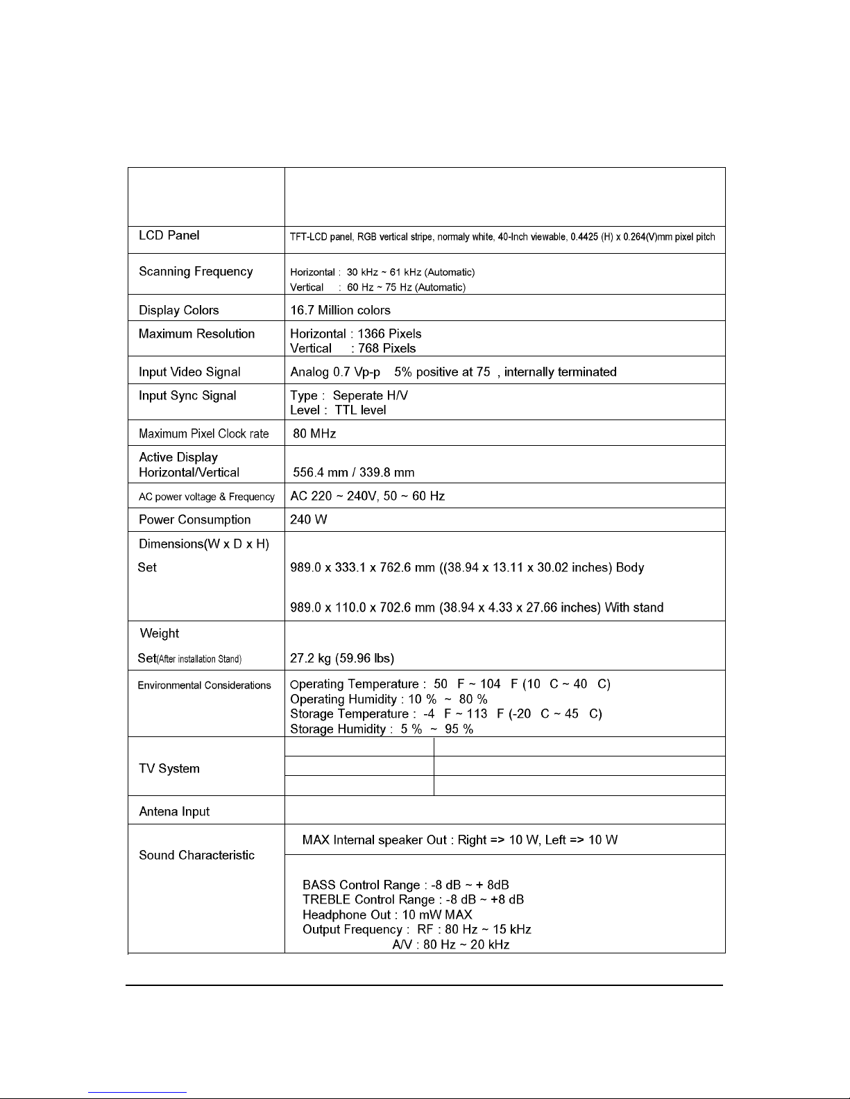
2 Product Specifications
2-1
2 Product Specifications
2-1 LE23R41B Specifications
± Ω
° ° ° °
° ° ° °
–
–
–
–
–
System PAL, SECEM
Item
Description
556.4 mm / 339.8 mm
Tunning Frequency Synthesize
Sound MONO, STEREO, NICAM
75Ω
2-2 LE26R41B Specifications
2 Product Specifications
2-2
±
° ° ° °
° °
° °
–
–
–
–
–
System PAL, SECEM
Item
Description
556.4 mm / 339.8 mm
Tunning Frequency Synthesize
Sound MONO, STEREO, NICAM
75Ω
2 Product Specifications
2-3
± Ω
° ° ° °
° ° ° °
–
–
–
–
–
System PAL, SECEM
Item
Description
Tunning Frequency Synthesize
Sound MONO, STEREO, NICAM
2-3 LE32R41B Specifications
75Ω
2 Product Specifications
2-4
± Ω
° ° ° °
° ° ° °
–
–
–
–
–
System PAL, SECEM
Item
Description
Tunning Frequency Synthesize
Sound MONO, STEREO, NICAM
2-4 LE40R41B Specifications
75Ω
2 Product Specifications
2-5
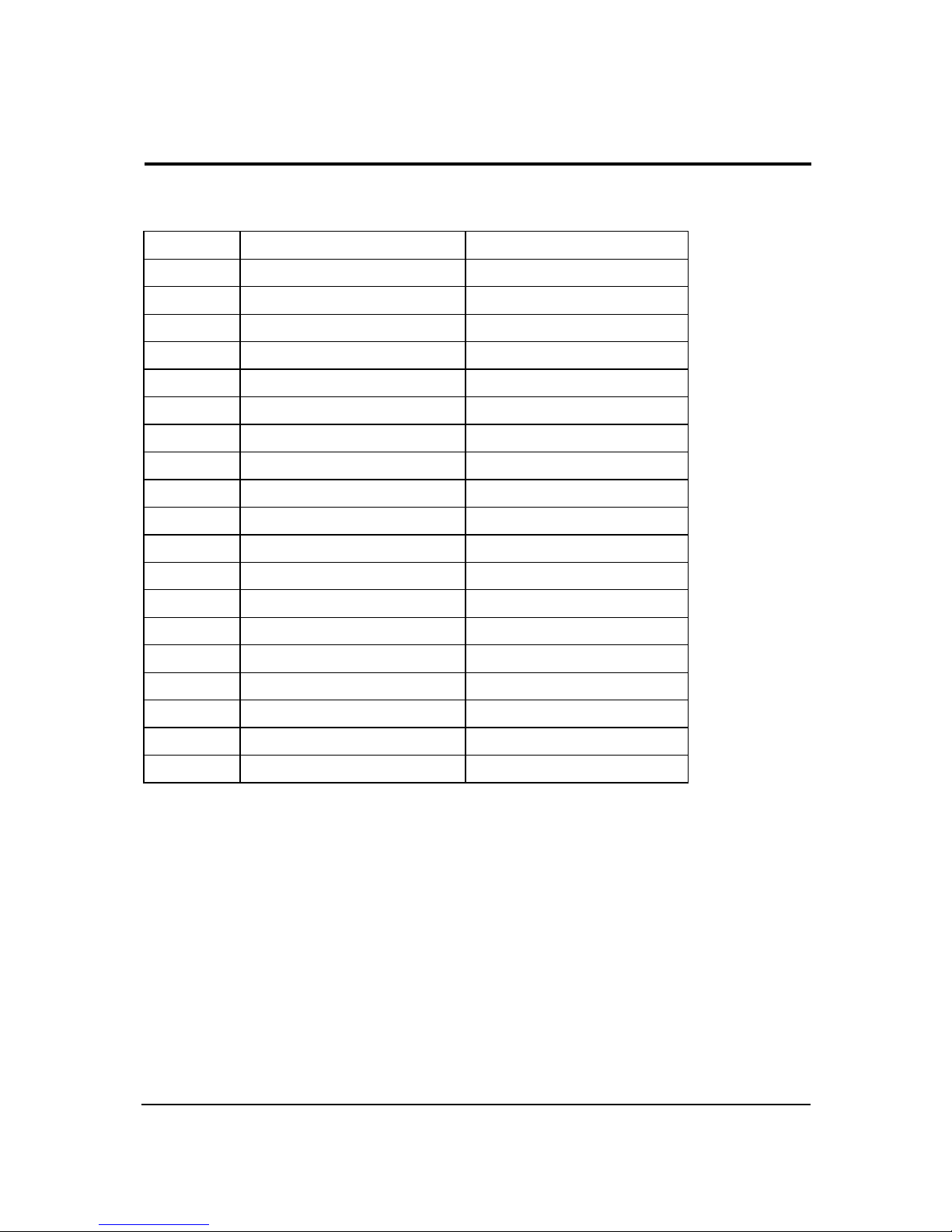
2-5 Pin Assignments
2-5-1 HDMI
Type A pin
1
2
3
4
5
6
7
8
9
10
11
12
13
14
15
16
17
18
19
Singnal Name
TMDS Data2+
TMDS Data2 Shield
TMDS Data2-
TMDS Data1+
TMDS Data2 Shield
TMDS Data1-
TMDS Data0+
TMDS Data0 Shield
TMDS Data0TMDS Clock+
TMDS Clock Shield
TMDS Clock-
CEC
Reserved (in cable but N.C on device)
SCL
SDA
DDC/CEC Ground
+5V Power
Hot Plug Delect
Wire
TMDS Signal wire
TMDS Shield
TMDS Signal wire
TMDS Signal wire
TMDS Shield
TMDS Signal wire
TMDS Signal wire
TMDS Shield
TMDS Signal wire
TMDS Signal wire
TMDS Clock Shield
TMDS Shield
Control
Control
Control
Control
Control
5 Volts Power wire
Control
2 Product Specifications
2-6
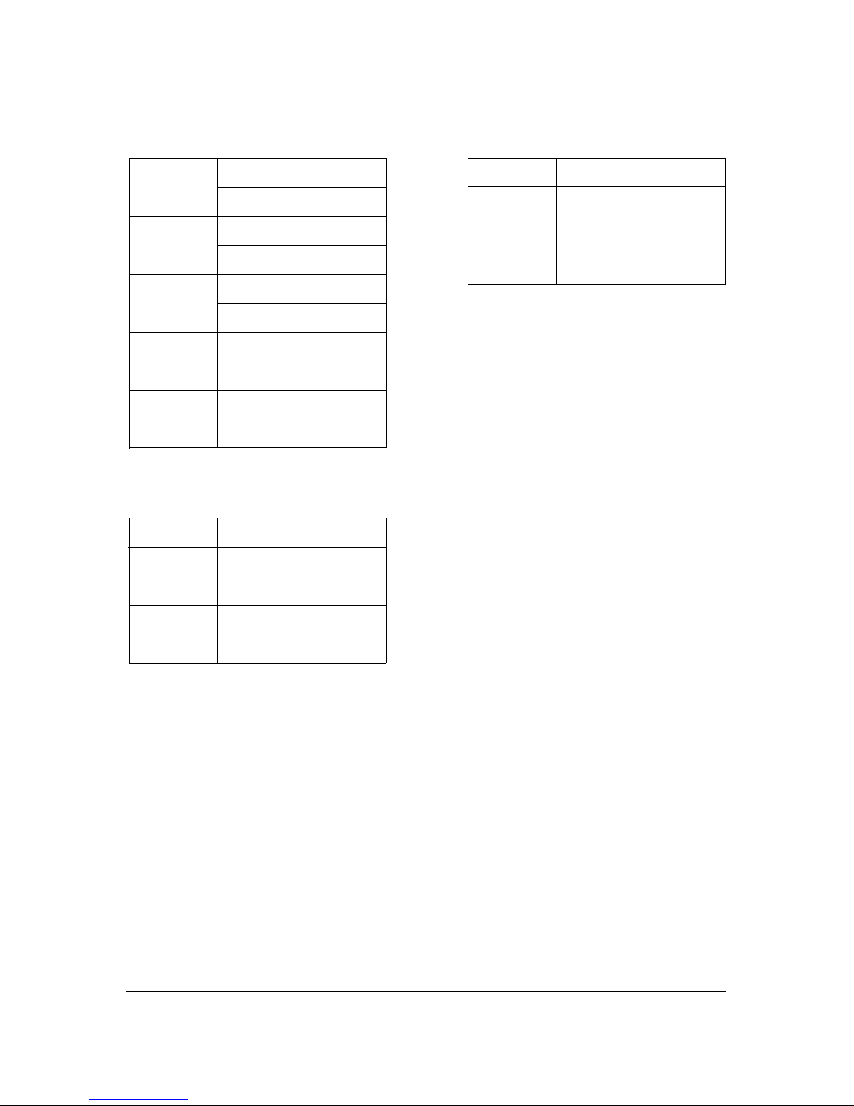
Pin
Separate
1
2
3
4
5
GND
Y
C
GND
GND
RCA Green
RCA Blue
RCA Red
RCA White
RCA Red
Y
GND
Pb (Cb)
GND
Pr (Cr)
GND
Audio L
GND
Audio R
GND
2-5-3 S-Video
2-5-2 Component 1
RCA White
RCA Red
CVBS
Audio L
GND
Audio R
GND
2-5-4 A/V
RCA Yellow
 Loading...