

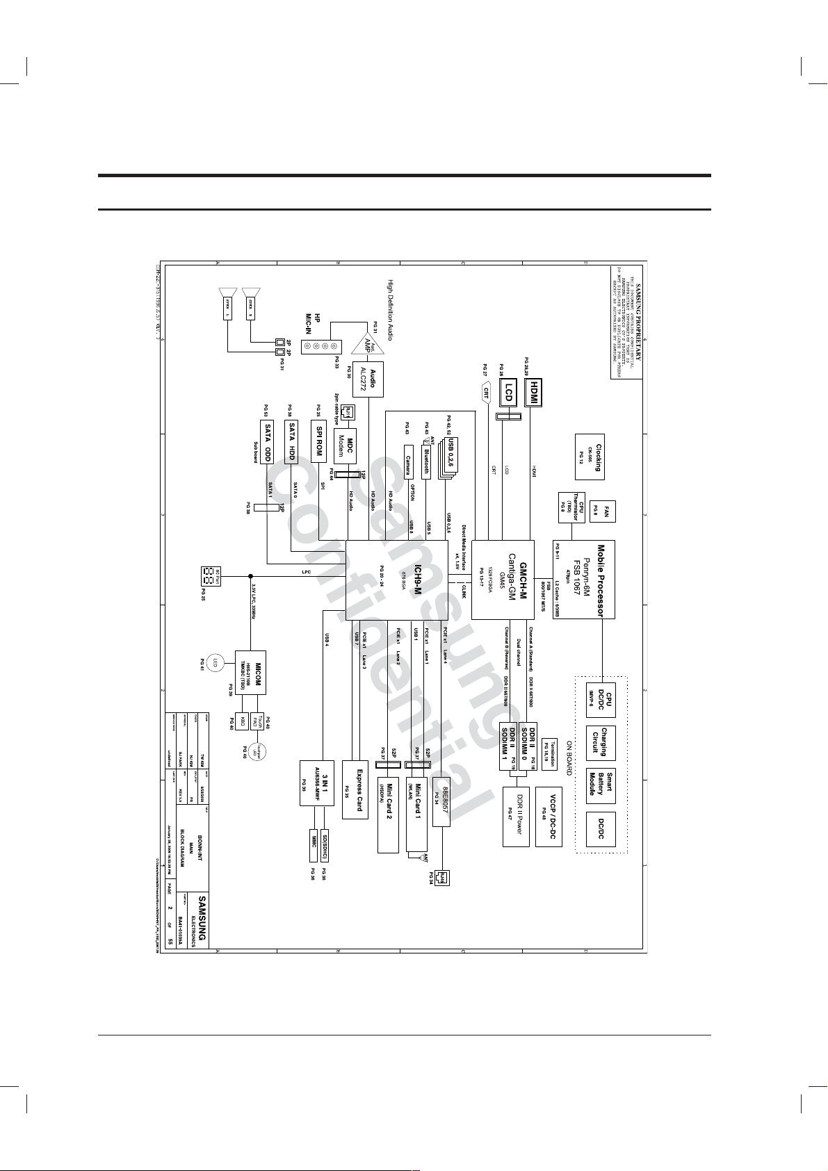
SAMSUNG R522 Schematic
- 이 문서는 삼성전자의 기술 자산으로 승인자만이 사용할 수 있습니다 -
www.vinafix.vn
- This Document can not be used without Samsung's authorization -
8. Block Diagram and Schematic
8-2
R522
- 이 문서는 삼성전자의 기술 자산으로 승인자만이 사용할 수 있습니다 -
www.vinafix.vn
- This Document can not be used without Samsung's authorization -
8. Block Diagram and Schematic
A A
8
9NC
6
7
Mini PCI Express 2
NC
4
3
Camera
See rev notes for more information.
2
DRAW
CHECK
APPROVAL
MODULE CODE
undefined
SJ PARK
TW KIM
HJ KIM
REV
DATE
DEV. STEP
LAST EDIT
9/23/2008
REV 1.0
PR
TITLE
January 28, 2009 18:53:26 PM
BOARD INFO
BONN-INT
MAIN
D:/Users/mobile29/mentor/Bonn/BONN-INT_PR_ESD_090129
1
PAGE OF
PART NO.
SAMSUNG
ELECTRONICS
BA41-01039A
553
B B
P5.0V_ALW 5.0V always power rail
P1.5V
VDC
VCC_CORE
P1.05V (VCCP)
P3.3V_AUX
P3.3V
P5.0V
P1.8V_AUX
P3.3V_MICOM
P0.9V
PORT # ASSIGNED TO
USB PORT Assign
0
1
5
2
3
SYSTEM PORT 0
SYSTEM PORT 2
NC4
SYSTEM PORT 1
Bluetooth
NC
PORT # ASSIGNED TO
PCI Express Assign
012
3
4
5
Mini Card 1 (WLAN)
LOM
NC
NC
NC
Mini Card 2 (ROBSON or DVB-T)
Confidential
Confidential
Confidential
5.0V switched on power rail (off in S4-S5)P5.0V_AUX
Samsung
Samsung
Samsung
REVISION HISTORY
GFX_CORE Core Voltage for GPU
3.3V always power rail (for Micom)
0.9V power rail for DDR (off in S3-S5)
Primary DC system power supply (7 to 21V)
1.5V switched power rail (off in S3-S5)
Core Voltage for CPU
3.3V switched on power rail (off in S4-S5)
1.8V power rail for DDR (off in S4-S5)
VTT for CPU, Crestline & ICH8-M
3.3V switched power rail (off in S3-S5)
5.0V switched power rail (off in S3-S5)
1.8V switched power rail (off in S3-S5)P1.8V
CPU Thermal Sensor
SODIMM0
CK-505M (Clock Generator) 1101 001x
I C / SMB Address
ICH8-m
SODIMM1
Thermal Sensor on SODIMM1
Voltage Rails
2
C C
A B-
Hub to PCI
LPC bridge/IDE/AC97/SMBUS
Internal MAC
C
LG
L
i
n
k
-
AD30(internal)
AD31(internal)
AD24(internal)
-NA
---
-
USB2.0 #2 (USB4) : C--
E
F
USB2.0 #3 (USB5) : E
USB2.0 #4 (EHCI) : H
LCD Pannel Detect
D
e
civ
e
25MHzCrystal NA
D
Cardbus
USB
ve
i
AD25
AD29(internal)
#LESDIsec
REQ/GNT#
3
A,B,C
Interrupts
USB2.0 #0 (USB0) : ABUSB2.0 #1 (USB1) : D
Crystal / Oscillator
TYPE FREQUENCY DEVICE
32.768KHzCrystal
14.318MHzCrystal
10MHzCrystal 0
D
DO NOT DISCLOSE TO OR DUPLICATE FOR OTHERS
SAMSUNG ELECTRONICS CO’S PROPERTY.
EXCEPT AS AUTHORIZED BY SAMSUNG.
SCHEMATIC ANNOTATIONS AND BOARD INFORMATION
PCI Devices
BOARD INFORMATION
1010 000x
1010 010x
Master
0111 101x
0011 010x 34h -
7Ah
A4h
D2h
A0h
30hThermal Sensor on SODIMM0 0011 000x
Thermal Sensor
--Clock, Unused Clock Output Disable
-
sserddAseciveD
-
Hex
Bus
SMBUS Master
loseRs
u
(TBD)
t
ICH8-M
L
CLOCK-Generator CK-505
MOCIM
NNAPnoi
LE
TCETED_
_
0
nINA
t
le
L
USAGE
Real Time Clock
H
D
46
F
612
9
/
2
1
6
D
THIS DOCUMENT CONTAINS CONFIDENTIAL
PROPRIETARY INFORMATION THAT IS
SAMSUNG PROPRIETARY
4
3
2
1
R522
8-3
 Loading...