

Samsung E1360m Troubleshooting
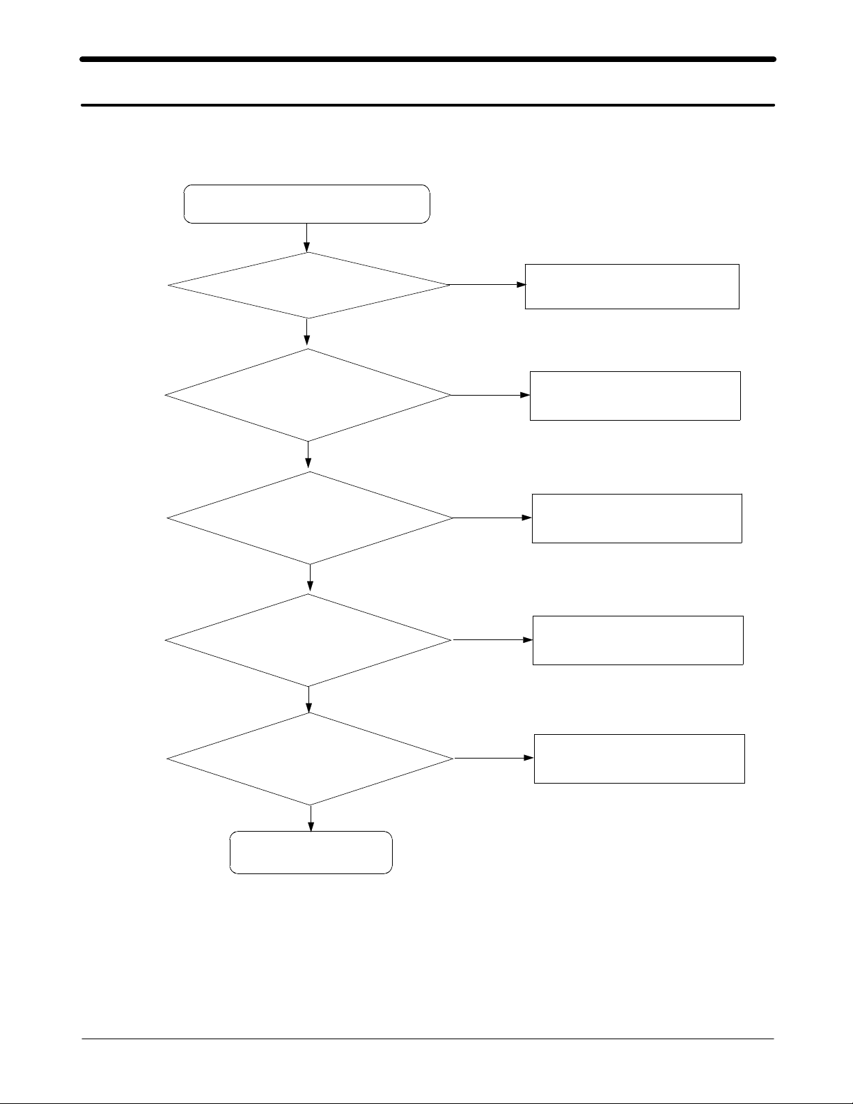
9. Flow Chart of Troubleshooting
Power On
9-1.
OWER ON' does not work
'P
Yes
Check battery voltage
is higher than
Check VPERM_3.0V,
VANA_2.85V, VRF_2.85V,
VSIM_3.0V, VMEM_1.8V,
VGPIO_2.8V of UME200
Check the pin1of
OSC200 produces clock
signal
Check the R312
concerning about Jig
Power on
3.3V
OK
OK
OK
Not OK
NotOK
Not OK
Not OK
Change battery
Check the UCP200
older OSC200 again
S
older R312 again
S
OK
No
Is Power On working?
Yes
END
Repeat sequence
9-1
SAMSUNG Proprietary-Contents may change without notice
This Document can not be used without Samsung's authorization
Flow Chart of Troubleshooting
NBE0
NBE1
NCS0
NCS1
NCS2
PCM_CLK
PCM_DI
PCM_DO
PCM_SYNC
PMU_VIO
PMU_VANA
PMU_VMEM
PMU_VPERM
PMU_VRF
PMU_VSIM
POK_IN
POK_OUT
PWM_OUT0
PWM_OUT1
PWM_OUT2
ICHGN
ICHGP
RFID_N
RFID_P
RFIL_N
RFIL_P
RFIP_N
RFIP_P
RFOH
RFOL
UART0_RD
UART0_TD
UART1_RD
UART1_TD
UART1_CTS
UART1_RTS
XTAL_26M_1
XTAL_26M_2
XTAL_32K_1
XTAL_32K_2
XTAL_SHLD
XTAL_SHLD
XTAL_SHLD
XTAL_SHLD
XTAL_SHLD
XTAL_SHLD
SIM_CLK
SIM_DATA
SIM_RST
SSI_CLK
SSI_DATA
SSI_OUT
SSI_SEL0
SSI_SEL1
SSI_SEL2
D11
E12
A12
B12
A11
H15
H16
W15
W14
V15
W12
W13
V14
K18
K19
H19
H18
G16
VGPIO_2.8V
LB
VANA_2.85V
VMEM_1.8V
UB
LCD_CS
NCSFLASH
NCSRAM
J19
J18
T8
V8
T7
T5
T6
W8
W9
E1
D1
G1
F1
C1
B1
R222
A1
A2
L18
W5
V5
V7
W6
A7
A6
L19
B8
A8
B6
A5
B7
B5
DCL
DD
FSC
ONKEY_2
ONKEY_1
ICHGN
ICHGP
DCSRX_N
DCSRX_P
EGSMRX_N
EGSMRX_P
DCS_TX
EGSM_TX
UART0_TD
UART0_RD
UART1_RD
UART1_TD
UART1_CTS
UART1_RTS
R223
DU
C207
C209
C210
VPERM_3.0V
VSIM_3.0V
VRF_2.85V
C211
C212
3
2
4
1
4
1
OSC201
2
3
OSC200
C214
SIM_CLK
SIM_DATA
SIM_RST
T1
U1
U2
R1
J2
T2
R_INT
BUS_ENABLE
LCD_BL_EN
C229
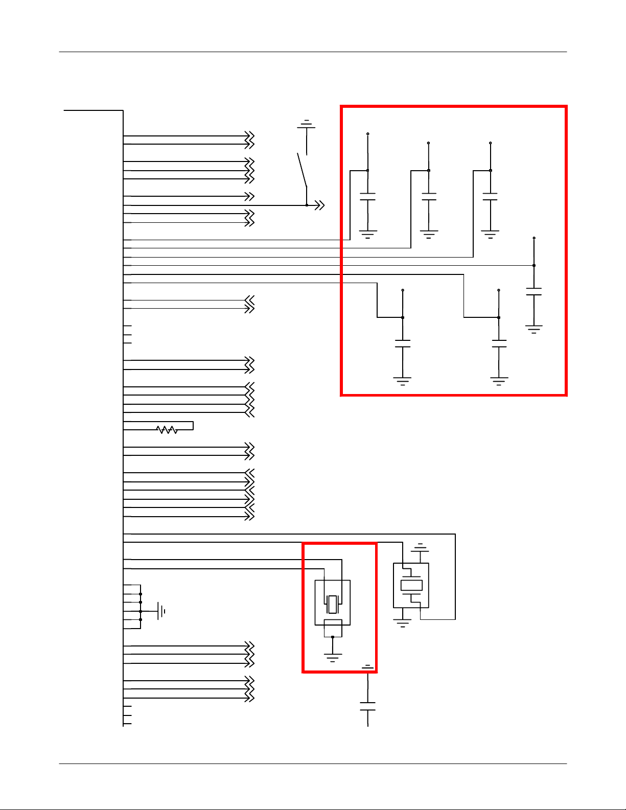
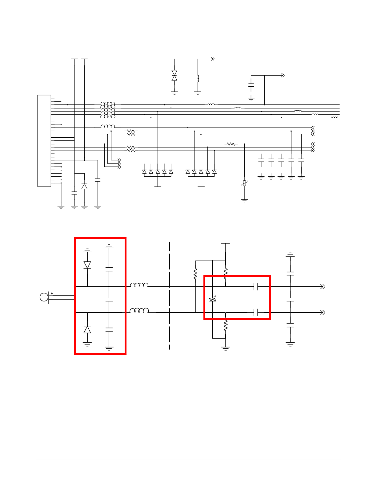
9-2
SAMSUNG Proprietary-Contents may change without notice
This Document can not be used without Samsung's authorization
VBAT
VCHG_5V
Flow Chart of Troubleshooting
FM_ANT
IFC300
C309
EAR_SW
C336
L318
C337
L319
AUX_DET
UART1TD
UART1RD
JIG_ON
UART0_TD
UART0_RD
ZD301
1
1
2
2
3
3
4
4
5
5
6
6
7
7
8
8
9
9
10
10
11
11
12
12
13
13
14
14
15
15
16
16
17
17
18
18
19
19
20
20
21
NC
22
NC
23
NC
24
NC
25
NC
26
NC
27
NC
ZD300
C310
C313
L301
L302
L303
L304
L305
L306
R314
UART1_TD_IF
UART1_RD_IF
JIG_ON_IF
R313
R309
R310
6
5
4
123
D302
L300
C300
L316
5
6
4
D303
L317
R312
C308
C307
123
VR300
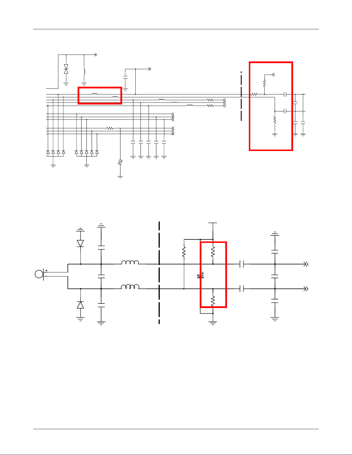
Digital External Interface- UART
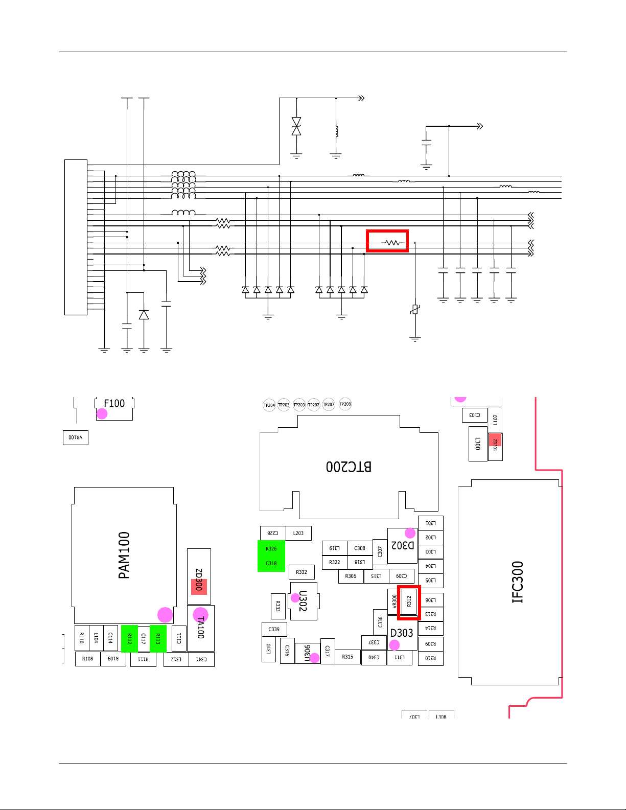
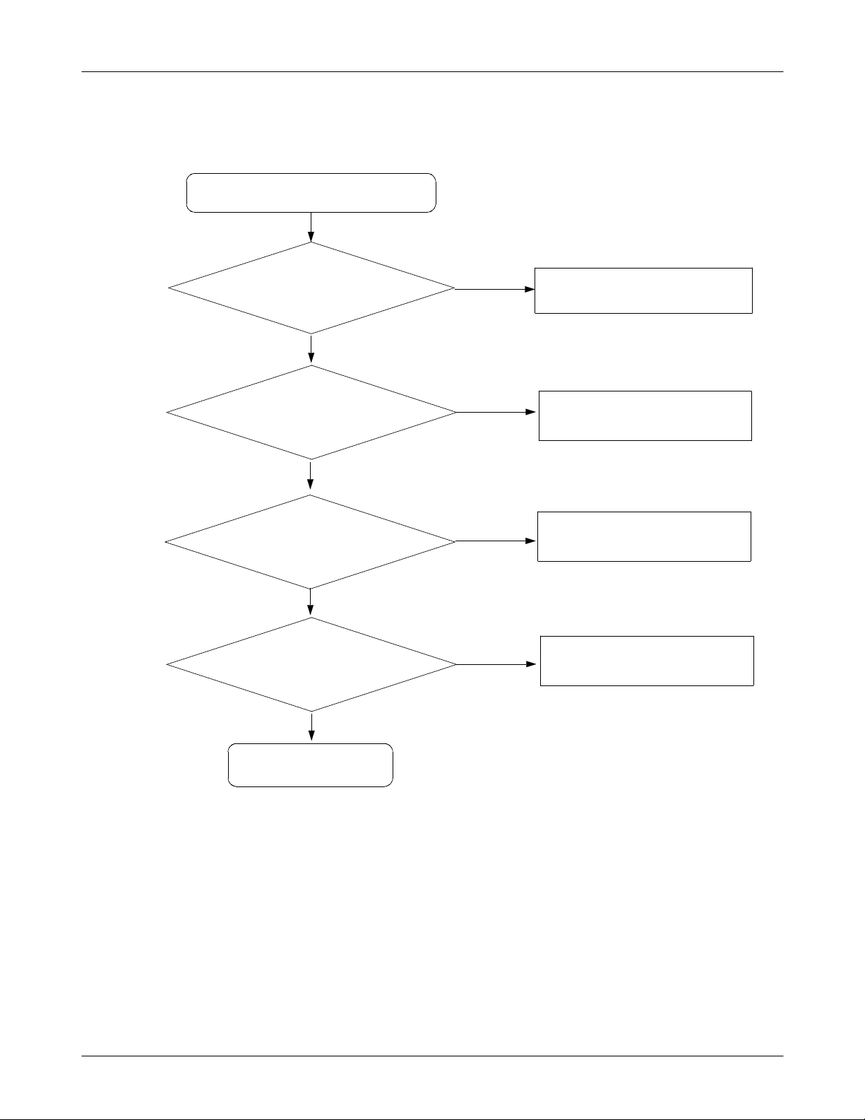
9-3
SAMSUNG Proprietary-Contents may change without notice
This Document can not be used without Samsung's authorization
Flow Chart of Troubleshooting
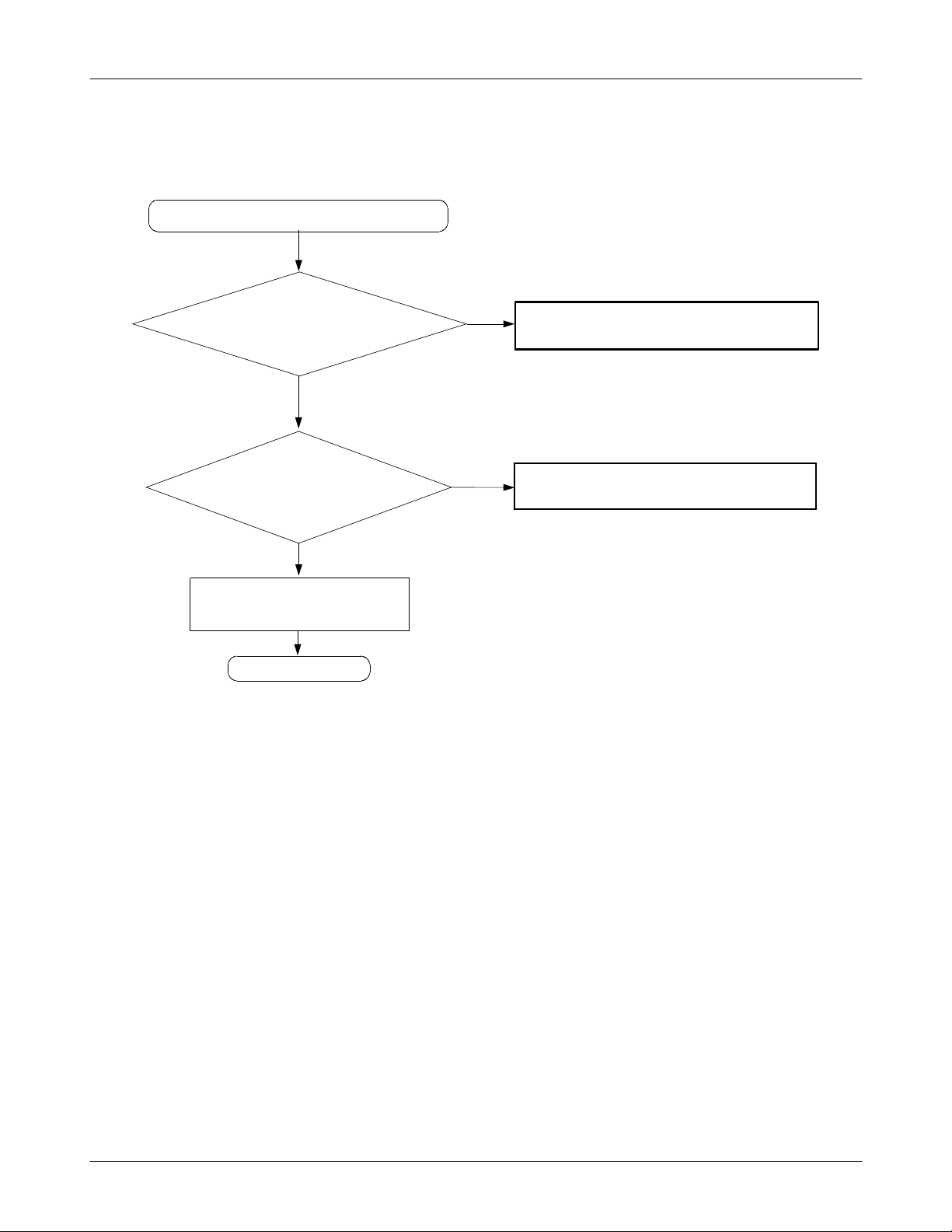
9-2. S
IM Part
Insert SIM" is displayed on the LCD
"
VSIM_3.0V at the pin#1
SIM
400
Is there any signal pin
#2,3,6
="
Yes
of SIM
Yes
H"?
400
No
No
?
Check the SIM Power
Check UCP200
Check the SIM Card
END
9-4
SAMSUNG Proprietary-Contents may change without notice
This Document can not be used without Samsung's authorization
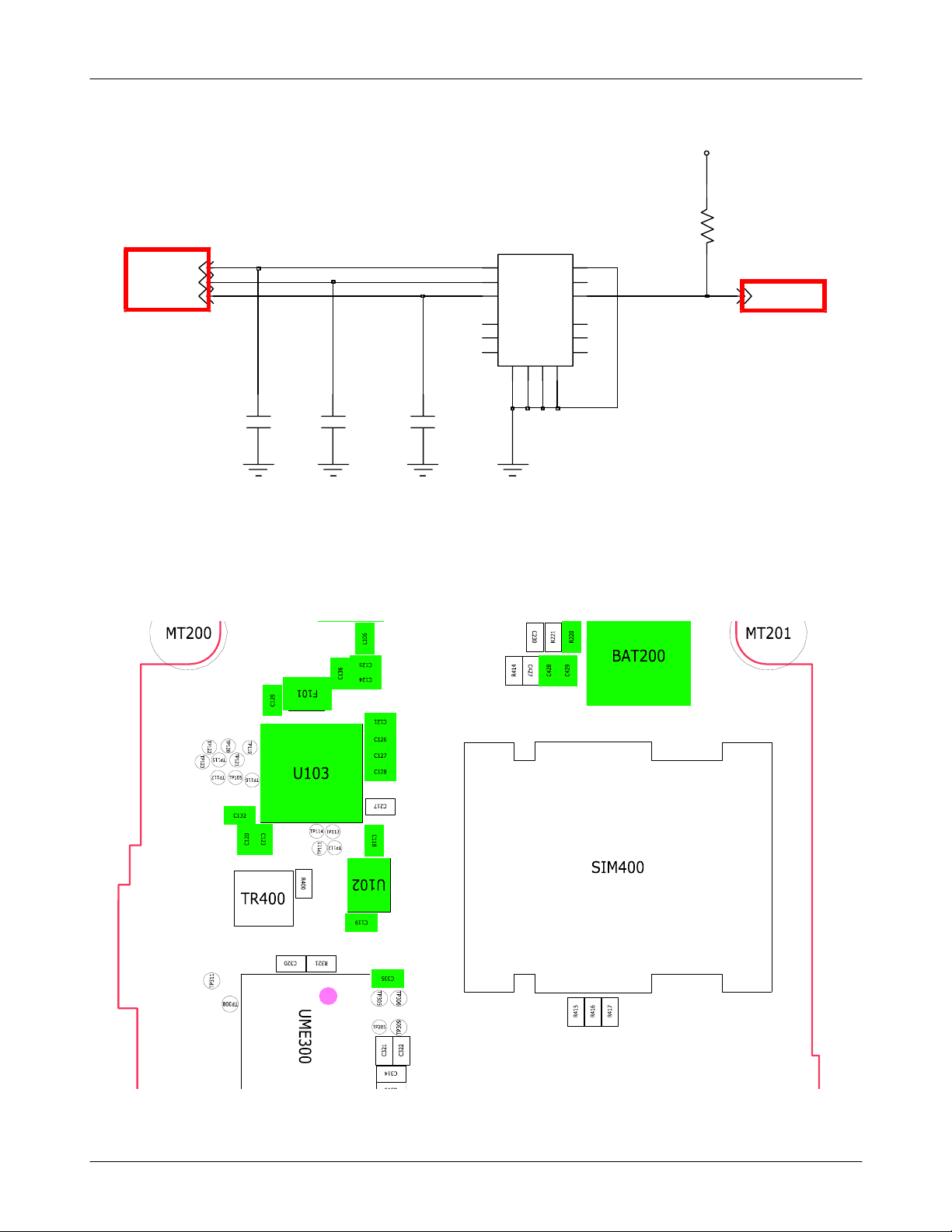
VSIM_3.0V
SIM_RST
SIM400
11
22
33 4
7
7
88
99
6
5
11 11
10 10
G
G
GG
1516
1314
Flow Chart of Troubleshooting
VSIM_3.0V
R414
6
5
4
1212
SIM_DATASIM_CLK
C427
C428
C429
SIM CONNECTOR
9-5
SAMSUNG Proprietary-Contents may change without notice
This Document can not be used without Samsung's authorization
Flow Chart of Troubleshooting
Microphone Part-Phone MIC
9-3.
Phone MIC does not work
Yes
Check the connection
of MIC
OK
Check thecomponents
which are connected to
MIC_BIAS
OK
Check the circuit
of MIC PART
OK
Is Phone MIC working?
Not OK
Not OK
Not OK
No
S
older MIC again
S
older
C328, C331
older
S
D304,D305,C326,C329,C333
Replace MIC
and TA300 again
Yes
END
9-6
SAMSUNG Proprietary-Contents may change without notice
This Document can not be used without Samsung's authorization
VBAT
L
VCHG_5V
Flow Chart of Troubleshooting
FM_ANT
IFC300
C309
EAR_SW
C336
L318
C337
L319
AUX_DET
UART1TD
UART1RD
JIG_ON
UART0_TD
UART0_RD
ZD301
1
1
2
2
3
3
4
4
5
5
6
6
7
7
8
8
9
9
10
10
11
11
12
12
13
13
14
14
15
15
16
16
17
17
18
18
19
19
20
20
21
NC
22
NC
23
NC
24
NC
25
NC
26
NC
27
NC
ZD300
C310
C313
L301
L302
L303
L304
L305
L306
R314
UART1_TD_IF
UART1_RD_IF
JIG_ON_IF
R313
R309
R310
6
5
4
123
D302
L300
C300
L316
5
6
4
D303
L317
R312
C308
C307
123
VR300
Digital External Interface- UART
MIC_BIAS
MIC300
D305
D304
C326
C329
C333
R331
L307
L308
MAIN_MIC
TA300
R329
R330
C327
C328
MIC_P
C330
C331
MIC_N
C332
9-7
SAMSUNG Proprietary-Contents may change without notice
This Document can not be used without Samsung's authorization
Flow Chart of Troubleshooting
Microphone Part-Earphone MIC
9-4.
Earphone MIC does not work
Yes
Check the connection
of IFC300
OK
Check MIC_BIAS.
When UME300 operates
(
and call is connected
OK
Check the circuit
of EAR MIC
OK
Is Earphone MIC working?
)
Not OK
Not OK
Not OK
No
older pin3of IFC300 again
S
older C302,C304 and R301 again and
S
older
S
check UCP200
R301,R329,R330,L316,L317,
L301 and L302 again
Repeat the sequence
Yes
END
9-8
SAMSUNG Proprietary-Contents may change without notice
This Document can not be used without Samsung's authorization
3
FM_ANT
Flow Chart of Troubleshooting
C308
C309
EAR_SW
C336
L318
C337
L319
AUX_DET
UART1TD
UART1RD
JIG_ON
UART0_TD
UART0_RD
L315
R322
R306
EAR_P
VCM_OUT
EAR_N
R303
R301
EAR_SW_REF
C302
C304
R311
C305
C303
C
ZD301
5
4
123
D302
L300
C300
L316
5
6
4
D303
L317
R312
C307
123
VR300
Digital External Interface- UART
MIC_BIAS
MIC300
D305
D304
C333
C326
C329
R331
L307
L308
MAIN_MIC
TA300
R329
R330
C327
C328
MIC_P
C330
C331
MIC_N
C332
9-9
SAMSUNG Proprietary-Contents may change without notice
This Document can not be used without Samsung's authorization
Flow Chart of Troubleshooting
Earphone Part
9-5.
Earphone does not work
Yes
Check the circuit
of IFC300
OK
Check the UCP200
Pin R19, T19
Check EAR SW
Ok
END
Not OK
Not OK
Not OK
older pin
S
L303, L304, L305, R303
again and check UCP200
Solder UCP200 or replace UCP200
Solder R301again
5,6,7
of IFC300
9-10
SAMSUNG Proprietary-Contents may change without notice
This Document can not be used without Samsung's authorization

Flow Chart of Troubleshooting
VANA_2.85V
TH200
R203
JIG_ON
EAR_P
SPK_N
SPK_P
C232
EAR_N
D(9)
D(10)
D(11)
D(12)
D(13)
VGPIO_2.8V
SCL
SDA
D200
D(14)
D(15)
5
KEY_EN
6
1
1
2
2
R
R
UART_SW
BT_LDO_EN
MONO_SEL
R219
SYS_CLK_REQ
BT_RST
VIB_EN
D201
FM_L
FM_R
5
0
0
1
4
0
2
R
C215
C231
MIC_BIAS
MIC_N
MIC_P
EAR_MIC_N
EAR_MIC_P
C216
0.2mm
C218
R206
EAR_SW
EAR_SW_REF
KEYIN(0)
KEYIN(1)
KEYIN(2)
DATA9
E18
DATA10
D18
DATA11
B17
DATA12
B18
DATA13
A19
DATA14
C18
DATA15
W4
GPIO1
V2
GPIO2
W2
GPIO5
V3
GPIO6
V4
G4
H5
W3
H4
J1
W1
V1
J4
R8
M19
N16
P18
R18
W16
W17
T18
U19
V19
U18
R19
T19
W18
W19
P19
N19
K1
K2
K4
determine VIO voltage level
GPIO7
GPIO8
GPIO10
GPIO20
GPIO38
GPIO39
GPIO40
GPIO41
GPIO57
AUX_POK
AUXADC0
AUXADC1
AUXAUD_IN_L
AUXAUD_IN_R
EAR_OUT_N|R
EAR_OUT_P|L
INTMIC_BIAS
INTMIC_IN_N
INTMIC_IN_P
EXTMIC_BIAS
EXTMIC_IN_N
EXTMIC_IN_P
HSET_OUT_N
HSET_OUT_P
HKSW_DET1
HKSW_DET2
KEYIN0
KEYIN1
KEYIN2
UCP200
IFC300
VBAT
VCHG_5V
ZD301
1
1
2
2
3
3
4
4
5
5
6
6
7
7
8
8
9
9
10
10
11
11
12
12
13
13
14
14
15
15
16
16
17
17
18
18
19
19
20
20
21
NC
22
NC
23
NC
24
NC
25
NC
26
NC
27
NC
ZD300
C310
C313
L301
L302
L303
L304
L306
R314
L305
UART1_TD_IF
UART1_RD_IF
JIG_ON_IF
R313
R309
R310
6
5
4
D302
6
123
FM_ANT
C309
EAR_SW
C336
C337
L318
L319
AUX_DET
UART1TD
UART1RD
JIG_ON
UART0_TD
UART0_RD
L315
R322
R306
EAR_P
VCM_OUT
EAR_N
L300
L316
5
4
123
D303
R312
L317
C300
C308
C307
VR300
Digital External Interface- UART
9-11
SAMSUNG Proprietary-Contents may change without notice
This Document can not be used without Samsung's authorization
 Loading...