

Samsung DVD-812, DVD-811, DVD-818, DVD-819, DVD-711 Service Manual
...
DVD PLAYER
DVD-811/812/818/819
DVD-711/718
DVD-818J
SERVICE
1. Precautions
2. Reference Information
3. Product Specification
4. Disassembly and Reassembly
5. Circuit Descriptions
6. Troubleshooting
7. Exploded Views and Parts List
8. Electrical Parts List
9. Block Diagrams
10. PCB Diagrams
11. Wiring Diagram
12. Schematic Diagrams
Manual
DVD PLAYER CONTENTS
SERVICE MANUAL DVD-811/812/818/819/711/718/818J
DVD-811/812/818/819/711/718/818J
DVD-711 (U.S.A/CANADA ONLY)
PLAY/PAUSE
OPEN/CLOSE
SKIPSTOP
STANDBY/ON
PLAY/PAUSE
OPEN/CLOSE
SKIPSTOP
STANDBY/ON
PHONES LEVEL
MIN MAX
ELECTRONICS
© Samsung Electronics Co., Ltd. AUG. 2000
Printed in Korea
AH68-00563A
Samsung Electronics 1-1
1. Precautions
1-1 Safety Precautions
1) Before returning an instrument to the customer,
always make a safety check of the entire instrument,
including, but not limited to, the following items:
(1) Be sure that no built-in protective devices are
defective or have been defeated during servicing.
(1)Protective shields are provided to protect both
the technician and the customer. Correctly replace
all missing protective shields, including any
remove for servicing convenience.
(2)When reinstalling the chassis and/or other assembly in the cabinet, be sure to put back in place
all protective devices, including, but not limited to,
nonmetallic control knobs, insulating fish papers,
adjustment and compartment covers/shields, and
isolation resistor/capacitor networks. Do not operate this instrument or permit it to be operated without all protective devices correctly installed and
functioning.
(2) Be sure that there are no cabinet openings through
which adults or children might be able to insert
their fingers and contact a hazardous voltage. Such
openings include, but are not limited to, excessively wide cabinet ventilation slots, and an improperly fitted and/or incorrectly secured cabinet back
cover.
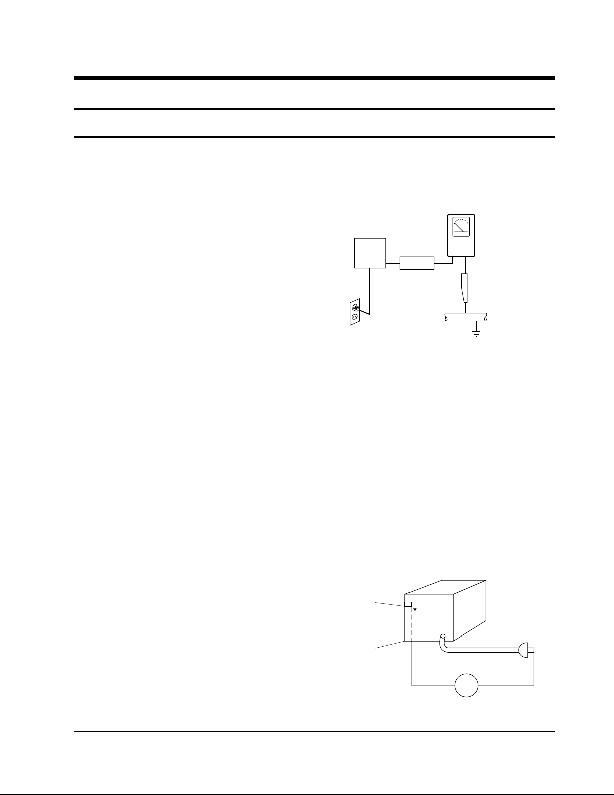
(3) Leakage Current Hot Check-With the instrument
completely reassembled, plug the AC line cord
directly into a 120V AC outlet. (Do not use a isolation transformer during this test.) Use a leakage
current tester or a metering system that complies
with American National Standards institute (ANSI)
C101.1 Leakage Current for Appliances and
Underwriters Laboratories (UL) 1270 (40.7). With
the instrument’s AC switch first in the ON position
and then in the OFF position, measure from a
known earth ground (metal water pipe, conduit,
etc.) to all exposed metal parts of the instrument
(antennas, handle brackets, metal cabinets, screwheads, metallic overlays, control shafts, etc.), especially any exposed metal parts that offer an electrical return path to the chassis.
Any current measured must not exceed 0.5mA.
Reverse the instrument power cord plug in the outlet and repeat the test. See Fig. 1-1.
Any measurements not within the limits specified
herein indicate a potential shock hazard that must
be eliminated before returning the instrument to
the customer.
Fig. 1-1 AC Leakage Test
(4) Insulation Resistance Test Cold Check-(1) Unplug
the power supply cord and connect a jumper wire
between the two prongs of the plug. (2) Turn on the
power switch of the instrument. (3) Measure the
resistance with an ohmmeter between the
jumpered AC plug and all exposed metallic cabinet
parts on the instrument, such as screwheads,
antenna, control shafts, handle brackets, etc. When
an exposed metallic part has a return path to the
chassis, the reading should be between 1 and 5.2
megohm. When there is no return path to the chassis, the reading must be infinite. If the reading is
not within the limits specified, there is the possibility of a shock hazard, and the instrument must be
re-pared and rechecked before it is returned to the
customer. See Fig. 1-2.
Fig. 1-2 Insulation Resistance Test
DEVICE
UNDER
TEST
(READING SHOULD
NOT BE ABOVE
0.5mA)
LEAKAGE
CURRENT
TESTER
EARTH
GROUND
TEST ALL
EXPOSED METER
SURFACES
ALSO TEST WITH
PLUG REVERSED
(USING AC ADAPTER
PLUG AS REQUIRED)
2-WIRE CORD
Antenna
Terminal
Exposed
Melal Part
ohm
ohmmeter

Precautions
1-2 Samsung Electronics
2) Read and comply with all caution and safety related notes non or inside the cabinet, or on the chassis.
3) Design Alteration Warning-Do not alter of add to
the mechanical or electrical design of this instrument. Design alterations and additions, including
but not limited to, circuit modifications and the
addition of items such as auxiliary audio output
connections, might alter the safety characteristics of
this instrument and create a hazard to the user. Any
design alterations or additions will make you, the
service, responsible for personal injury or property
damage resulting therefrom.
4) Observe original lead dress. Take extra care to
assure correct lead dress in the following areas:
(1) near sharp edges, (2) near thermally hot parts (be
sure that leads and components do not touch thermally hot parts), (3) the AC supply, (4) high voltage,
and (5) antenna wiring. Always inspect in all areas
for pinched, out-of-place, or frayed wiring, Do not
change spacing between a component and the
printed-circuit board. Check the AC power cord for
damage.
5) Components, parts, and/or wiring that appear to
have overheated or that are otherwise damaged
should be replaced with components, parts and/ or
wiring that meet original specifications.
Additionally, determine the cause of overheating
and/or damage and, if necessary, take corrective
action to remove any potential safety hazard.
6) Product Safety Notice-Some electrical and mechanical parts have special safety-related characteristics
which are often not evident from visual inspection,
nor can the protection they give necessarily be
obtained by replacing them with components rated
for higher voltage, wattage, etc. Parts that have special safety characteristics are identified by shading,
an ( )or a ( )on schematics and parts lists. Use
of a substitute replacement that does not have the
same safety characteristics as the recommended
replacement part might created shock, fire and/or
other hazards. Product safety is under review continuously and new instructions are issued whenever appropriate.

Precautions
Samsung Electronics 1-3
1-2 Servicing Precautions
CAUTION : Before servicing Instruments covered
by this service manual and its supplements, read and
follow the Safety Precautions section of this manual.
Note : If unforseen circument create conflict between
the following servicing precautions and any of the
safety precautions, always follow the safety precautions. Remember: Safety First.
1-2-1 General Servicing Precautions
(1) a. Always unplug the instrument’s AC power cord
from the AC power source before (1) re-moving
or reinstalling any component, circuit board,
module or any other instrument assembly, (2)
disconnecting any instrument electrical plug or
other electrical connection, (3) connecting a test
substitute in parallel with an electrolytic capacitor in the instrument.
b. Do not defeat any plug/socket B+ voltage inter-
locks with which instruments covered by this
service manual might be equipped.
c. Do not apply AC power to this instrument and
/or any of its electrical assemblies unless all
solid-state device heat sinks are correctly installed.
d. Always connect a test instrument’s ground lead
to the instrument chassis ground before connecting the test instrument positive lead. Always
remove the test instrument ground lead last.
Note : Refer to the Safety Precautions section ground
lead last.
(2) The service precautions are indicated or printed on
the cabinet, chassis or components. When servicing, follow the printed or indicated service precautions and service materials.
(3) The components used in the unit have a specified
flame resistance and dielectric strength.
When replacing components, use components
which have the same ratings. Components i-entified by shading, by( ) or by ( ) in the circuit diagram are important for safety or for the characteristics of the unit. Always replace them with the exact
replacement components.
(4) An insulation tube or tape is sometimes used and
some components are raised above the printed
wiring board for safety. The internal wiring is
sometimes clamped to prevent contact with heating components. Install such elements as they
were.
(5) After servicing, always check that the removed
screws, components, and wiring have been installed correctly and that the portion around the
serviced part has not been damaged and so on.
Further, check the insulation between the blades of
the attachment plug and accessible conductive
parts.
1-2-2 Insulation Checking Procedure
Disconnect the attachment plug from the AC outlet
and turn the power ON. Connect the insulation resistance meter (500V) to the blades of the attachment
plug. The insulation resistance between each blade of
the attachment plug and accessible conductive
parts(see note) should be more than 1 Megohm.
Note : Accessible conductive parts include metal panels, input terminals, earphone jacks, etc.

Precautions
1-4 Samsung Electronics
1-3 ESD Precautions
Electrostatically Sensitive Devices (ESD)
Some semiconductor (solid state) devices can be damaged easily by static electricity.
Such components commonly are called Electrostatically Sensitive Devices(ESD). Examples of typical ESD
devices are integrated circuits and some field-effect
transistors and semiconductor chip components. The
following techniques should be used to help reduce
the incidence of component damage caused by static
electricity.
(1) Immediately before handling any semiconductor
component or semiconductor-equipped assembly,
drain off any electrostatic charge on your body by
touching a known earth ground. Alternatively,
obtain and wear a commercially available discharging wrist strap device, which should be
removed for potential shock reasons prior to applying power to the unit under test.
(2) After removing an electrical assembly equipped
with ESD devices, place the assembly on a conductive surface such as aluminum foil, to prevent electrostatic charge buildup or exposure of the assembly.
(3) Use only a grounded-tip soldering iron to solder or
unsolder ESD devices.
(4) Use only an anti-static solder removal devices.
Some solder removal devices not classified as
“anti-static” can generate electrical charges sufficient to damage ESD devices.
(5) Do not use freon-propelled chemicals. These can
generate electrical charges sufficient to damage
ESD devices.
(6) Do not remove a replacement ESD device from its
protective package until immediately before your
are ready to install it.(Most replacement ESD
devices are packaged with leads electrically shorted together by conductive foam, aluminum foil or
comparable conductive materials).
(7) Immediately before removing the protective ma-
terials from the leads of a replacement ESD device,
touch the protective material to the chassis or circuit assembly into which the device will be
installed.
CAUTION : Be sure no power is applied to the chassis or circuit, and observe all other safety precautions.
(8) Minimize bodily motions when handling unpack-
aged replacement ESD devices. (Otherwise harmless motion such as the brushing together of your
clothes fabric or the lifting of your foot from a carpeted floor can generate static electricity sufficient
to damage an ESD device).
Precautions
Samsung Electronics 1-5
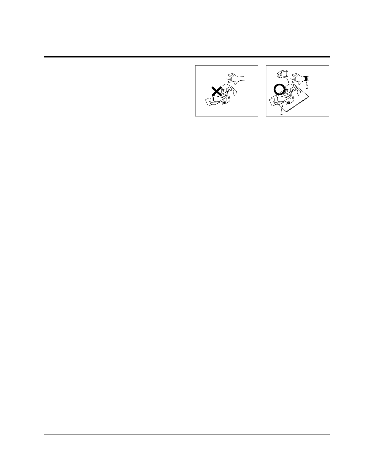
1-4 Handling the optical pick-up
The laser diode in the optical pick up may suffer electrostatic breakdown because of potential static electricity from clothing and your body.
The following method is recommended.
(1) Place a conductive sheet on the work bench (The
black sheet used for wrapping repair parts.)
(2) Place the set on the conductive sheet so that the
chassis is grounded to the sheet.
(3) Place your hands on the conductive sheet(This
gives them the same ground as the sheet.)
(4) Remove the optical pick up block
(5) Perform work on top of the conductive sheet. Be
careful not to let your clothes or any other static
sources to touch the unit.
◆ Be sure to put on a wrist strap grounded to the
sheet.
◆ Be sure to lay a conductive sheet made of copper etc.
Which is grounded to the table.
Fig.1-3
(6) Short the short terminal on the PCB, which is in-
side the Pick-Up ASS’Y, before replacing the PickUp. (The short terminal is shorted when the PickUp Ass’y is being lifted or moved.)
(7) After replacing the Pick-up, open the short termi-
nal on the PCB.
THE UNIT
WRIST-STRAP
FOR GROUNDING
1M
1M
CONDUCTIVE SHEET

Precautions
1-6 Samsung Electronics
1-5 Pick-up disassembly and reassembly
1-5-1 Disassembly
1) Remove the power cable.
2) Switch SW3 on Deck PCB to “OFF” before
removing the Flat-Cable.
( Inserted into Main PCB DCN1. See Fig. 1-4)
3) Disassemble the Deck.
4) Disassemble the Deck PCB.
1-5-2 Assembly
1) Replace the Pick-up.
2) Assemble the Deck PCB.
3) Reassemble the Deck.
4) Insert Flat-Cable into Main PCB DCN1 and switch
SW3 on Deck PCB to “ON”. (See Fig 1-4)
FLAT-CABLE
TO MAIN PCB
(DCN1)
Note : If the assembly and disassembly are not done in correct sequence, the Pick-up may be damaged.
Fig. 1-4
Samsung Electronics 2-1
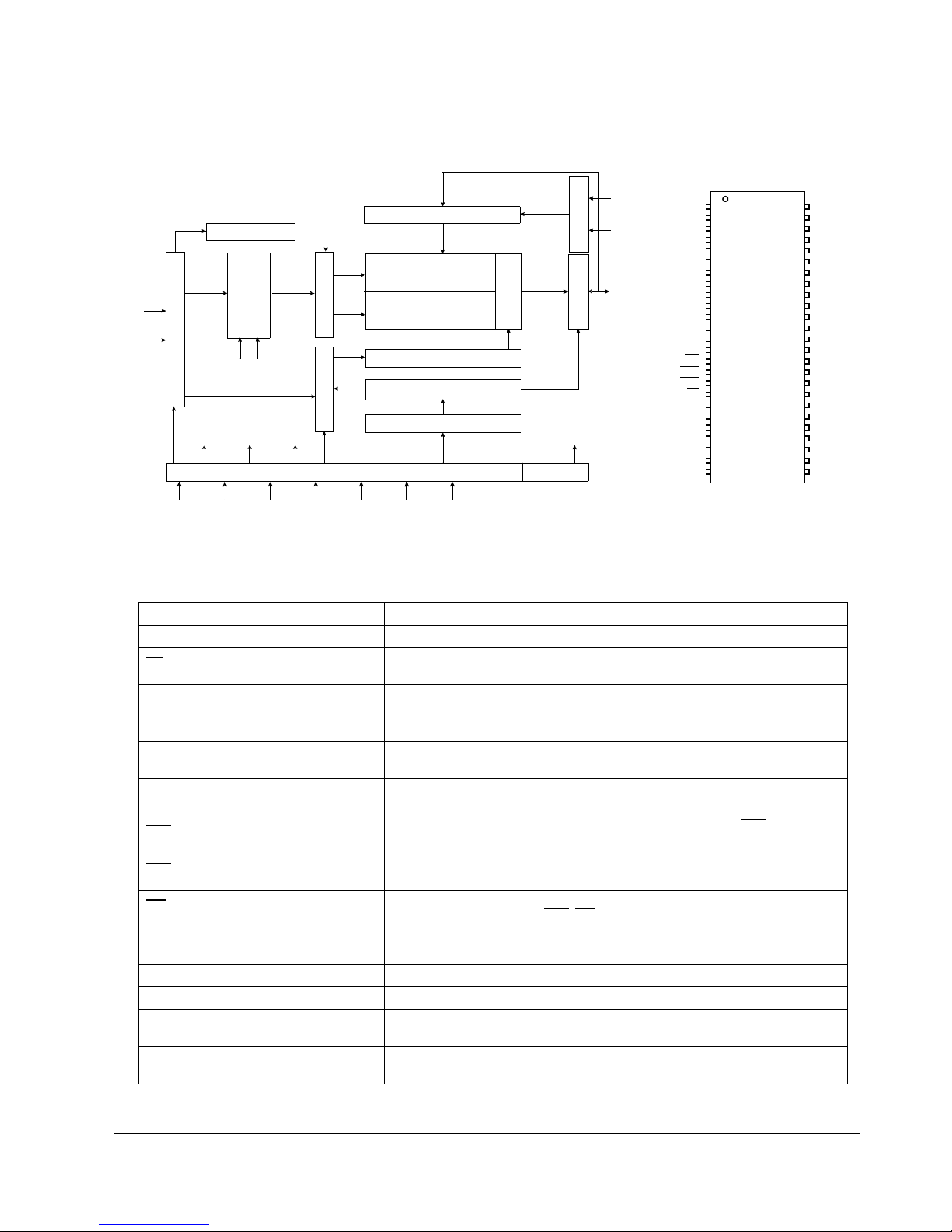
2. Reference Information
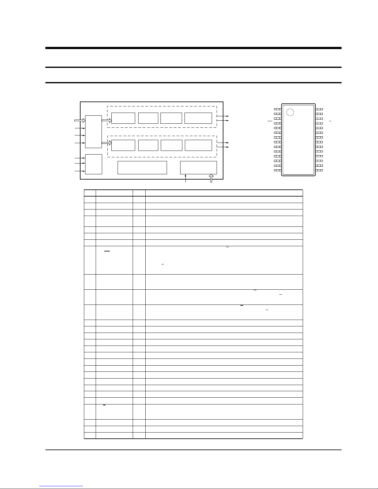
2-1 IC Descriptions
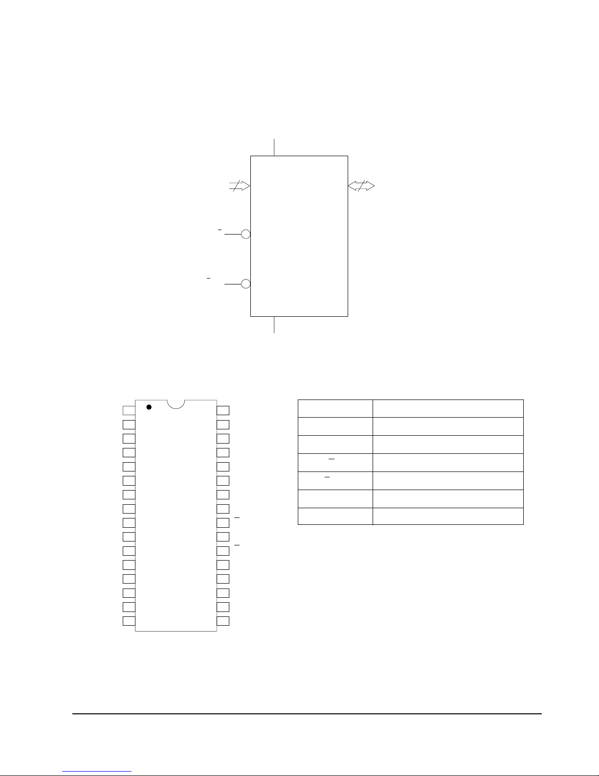
2-1-1 AIC1 (AK4393 ; Digital-to-Analog Converter)
Serial
Input
Interface
De-emphasis
Control
De-emphasis
Soft Mute
De-emphasis
Soft Mute
Left Channel
Right Channel
8X
Interpolator
8X
Interpolator
Multi-bit ˘•
Modulator
Multi-bit ˘•
Modulator
Switched
Capacitor Filter
Switched
Capacitor Filter
Control
Register
Double
Speed Select
Soft Mute
Power Down
Serial Data
Bit Clock
Left/Right Clock
Serial
Input Control
Clock Divider
Master Clock Clock Control
Left Output -
Left Output +
Right Output -
Right Output +
DVSS
DVDD
MCLK
PD
BICK
SDATA
LRCK
SMUTE
DFS
DEM0
DEM1
DIF0
1
2
3
4
5
6
7
8
9
10
11
12
DIF1
13
DIF2
CKS2
CKS1
CKS0
P/S
VCOM
AOUTL+
AOUTLAOUTR+
AOUTRAVSS
AVDD
VREFH
VREFL
BVSS
14
28
27
26
25
24
23
22
21
20
19
18
17
16
15
No. Pin Name I/O Pin Function and Description
1 DVSS - Digital Ground. Digital ground is 0V.
2 DVDD - Digital Supply. 3.3V or 5.0V nominal.
3 MCLK I Master Clock Input.
4 PD I Power-down and Reset. When low the AK4393 is in Power-down Mode and held in reset.
The AK4393 should always be reset after power-up.
5 BICK I Audio Serial Data Clock Input. A clock input of 64fs or more is recommended.
6
SDATA I
Serial Data Input.
7 LRCK I Left/Right Clock Input. Defines the sampling rate, F
s
.
8 SMUTE
(or CS
)
I Soft Mute Input or Chip Select Input. If the P/S
pin (pin 25) is high, SMUTE controls the
soft mute function as follows:
- When SMUTE goes high, the soft mute cycle is initiated.
- When SMUTE goes low, the output mute is slowly released.
If the P/S
pin is low, SMUTE is the Chip Select Input for the Serial Control Mode. Chip
select is active when SMUTE is low.
9 DFS I Double Sampling Speed Input. When low, this pin defines the Normal Speed Mode, and
128 x F
s
oversampling is implemented. When high, the DFS pin defines the Double Speed
Mode, implemented with 64 x F
s
oversampling. This pin features an internal pull-down.
10 DEM0
(or CCLK)
I De-emphasis Enable #0 or Control Data Clock Input. If the P/S
pin (pin 25) is high,
DEM0 is used to select the De-emphasis Mode according to Table 3. If the P/S pin os low
DEM0 is the clock input for the Serial Control Mode.
11 DEM1
(or CDTI)
I De-emphasis Enable #1 or Control Data Input. If the P/S
pin (pin 25) is high, DEM1 is
used to select the De-emphasis Mode according to Table 3. If the P/S pin is low, DEM1 is
the control data input for the Serial Control Mode.
12 DIF0 I Digital Input Format Select #0.
13 DIF1 I Digital Input Format Select #1.
14 DIF2 I Digital Input Format Select #2.
15 BVSS - Substrate Ground Pin. Substrate ground is 0V.
16 VREFL I Low Level Voltage Reference Input. Normally connected to analog ground.
17 VREFH I High Level Voltage Reference Input. Normally connected to analog supply.
18 AVDD - Analog Supply. Analog supply is 5V nominal.
19 AVSS - Analog Ground. Analog ground is 0V.
20 AOUTR- O Right Channel Negative Output.
21 AOUTR+ O Right Channel Positive Output.
22 AOUTL- O Left Channel Negative Output.
23 AOUTL+ O Left Channel Positive Output.
24 VCOM O Common Voltage Output. Common voltage output is 2.6V nominal.
25 P/S
I Parallel/Serial Control Mode Select Input. If Low, the Serial Control Mode is
implemented. If High, the Parallel Control Mode is selected. This pin has an internal
pull-up.
26 CKS0 I Master Clock Select #0.
27 CKS1 I Master Clock Select #1.
28 CKS2 I Master Clock Select #2.
Reference Information
2-2 Samsung Electronics
2-1-2 AIC2 (KS1456 ; 6CH. D/A Converter )
SCF
DAC
DATT
DZFL1
LOUT1+
LOUT1-
SCF
DAC
DATT
DZFR1
ROUT1+
ROUT1-
SCF
DAC
DATT
DZFL2
LOUT2+
LOUT2-
SCF
DAC
DATT
DZFR2
ROUT2
+
ROUT2-
SCF DAC
DATT
DZFL3
LOUT3+
LOUT3-
SCF DAC
DATT
DZFR3
ROUT3+
ROUT3-
Audio
I/F
Control
Register
AK4356
MCLK
LRCK
BICK
MCK
O
LRCK
BICK
XTI
XTO
Controller
CS
CCLK
CDTI
LRCK
BICK
SDOUT1
SDOUT2
SDOUT3
AC3
SDTI1
SDTI2
SDTI3
LOUT1-
ROUT
1+
1
LOUT1+
44
2
DZFL2 3
DZFR1 4
DZFL1
5
AD0 6
AD1 7
PDN 8
BICK
9
MCLK 10
DVDD 11
ROUT
1-43
LOUT
2+42
LOUT
2-41
ROUT
2+40
ROUT
2-
39
LOUT
3+38
LOUT
3-
37
ROUT
3+36
ROUT
3-35
AVSS
34
VSS
12
DTI
1
13
DTI
2
14
DTI
3
15
RCK
16
MUTE
17
CLK
18
DTI 19
CSN
20
FS
0
21
KS
0
22
33
32
31
30
29
28
27
26
25
24
23
AV DD
VREFH
DZFR2
DZFL3
DZFR3
DZFE
DIF2
DIF1
DIF0
CKS2
CKS1
AK4356VQ
Top View
No. Pin Name I/O Function
1 LOUT1- O DAC1 Lch Negative Analog Output Pin
2 LOUT1+ O DAC1 Lch Positive Analog Output Pin
3 DZFL2 O DAC2 Lch Zero Input Detect Pin
4 DZFR1 O DAC1 Rch Zero Input Detect Pin
5 DZFL1 O DAC1 Lch Zero Input Detect Pin
6 CAD0 I Chip Address 0 Pin
7 CAD1 I Chip Address 1 Pin
8 PDN I Power-Down & Reset Pin
When L , th e AK4356 is powered-down and the control registers are reset to
default state. If the state of CAD0-1 changes, then the AK4356 must be reset by PDN.
9 BICK I Audio Serial Data Clock Pin
10 MCLK I Master Clock Input Pin
11 DVDD -
Digital Power Supply Pin, +4.75~+5.25V
12 DVSS - Digital Ground Pin
13 SDTI1 I DAC1 Audio Serial Data Input Pin
14 SDTI2 I DAC2 Audio Serial Data Input Pin
15 SDTI3 I DAC3 Audio Serial Data Input Pin
16 LRCK I Audio Input Channel Clock Pin
17 SMUTE I Soft Mute Pin (Note)
When this pin goes to H , soft mute cycle is initialized.
When returning to L , the output mute releases.
18 CCLK I Control Data Clock Pin
19 CDTI I Control Data Input Pin
2021CSN I Chip Select Pin
This pin should be held to H except for access.
DFS0 I Double Speed Sampling Mode 0 Pin (Note)
L : Normal Speed, H : Double Speed at DFS1 bit = 0 .
22 CKS0 I Inpu
t Clock Select 0 Pin (Note)
23 CKS1 I Input Clock Select 1 Pin (Note)
24 CKS2 I Input Clock Select 2 Pin (Note)
25 DIF0 I Audio Data Interface Format 0 Pin (Note)
26 DIF1 I Audio Data Interface Format 1 Pin (Note)
27 DIF2 I Audio Data Interface Format 2 Pin (Note)
28 DZFE I Zero Input Detect Enable Pin (Note)
29 DZFR3 O DAC3 Rch Zero Input Detect Pin
30 DZFL3 O DAC3 Lch Zero Input Detect Pin
31 DZFR2 O DAC2 Rch Zero Input Detect Pin
32 VREFH I Positive Vo ltage Reference Input Pin, AVDD
33 AVDD - Analog Power Supply Pin
34 AVSS -
Analog Ground Pin, +4.75~+5.25V
35 ROUT3- O DAC3 Rch Negative Analog Output Pin
36 ROUT3+ O DAC3 Rch Positive Analog Output Pin
37 LOUT3- O DAC3 Lch Negative Analog Output Pin
38 LOUT3+ O DAC3 Lch Positive Analog Output Pin
39 ROUT2- O DAC2 Rch Negative Analog Output Pin
40 ROUT2+ O DAC2 Rch Positive Analog Output Pin
41 LOUT2- O DAC2 Lch Negative Analog Output Pin
42 LOUT2+ O DAC2 Lch Positive Analog Output Pin
43 ROUT1- O DAC1 Rch Negative Analog Output Pin
44 ROUT1+ O DAC1 Rch Positive Analog Output Pin

Reference Information
Samsung Electronics 2-3
2-1-3 DIC2 (KM416C254D ; CMOS 4M DRAM)
WE
CASL CAS
CASH
D0
D1
D2
D3
D4
D5
D6
D7
D8
RAS
NO.2 CLOCK
GENERATOR
CONTROL
LOGIC
COLUMN
DECODER
SENSE AMPLIFIERS
VO GATING
ROW
DECODER
512x512x16
MEMORY
ARRAY
512
512
DATA-IN BUFFER
DATA-OUT
BUFFER
REFRESH
CONTROLLER
REFRESH
COUNTER
NO.1CLOCK
GENERATOR
ROW.
ADDRESS
BUFFERS(9)
COLUMN
ADDRESS
BUFFER
OE
Vcc
Vss
IO0
IO15
16
9
88
99
9
9
16
512x16
PIN NO. SYM. TYPE DESCRITION
16~19, 22~26 A0~A8 Input Address Input
14 RAS Input Row Address Strobe
28 CASH Input Column Address Strobe/Upper Byte Control
29 CASL Input Column Address Strobe/Lower Byte Control
13 WE Input Write Enable
27 OE Input Output Enable
2~5, 7~10, 31~34, 36~39 I/O0~I/O15 Input/Output Data Input/Output
1, 6, 20 Vcc Supply Power, 5V
21, 35, 40 Vss Ground Ground
11, 12, 15, 30 NC - No Connect
Reference Information
2-4 Samsung Electronics
2-1-4 DIC1 (KS1453 ; Data Processor)
DVD CLV/CAV
16-8
DEMO D
32BIT SR
X-tal & Tim ing
Generator
Frame Sync
DET/PROT/ INS
(17.57KHz)
VCO Timing
Generator
MICOM I/F
(208,192,17)
(182,172,11)
ECC
Descrambler
(6,4,3)
efmwr ID ECC
EDC
17.58KHz= 26.16M/1488
RFCK 1 7.58/7 .35KHz
26.16MHz
676.08Hz
To MICOM (15)
MDAT[7:0]_BI, MRZA_IN, ZCS_IN, M WR_IN,
MRD_IN, ZIRQZD_OUT, ZWAIT_OUT, ZRST_IN
To DRAM
256K*16
(32 )
DD[15:0]_BI
DADR[8:0]_OUT
ZRAS_OUT
ZUCAS_OUT
ZLCAS _ OUT
ZOE[1 :0]_OUT
ZWE[1:0]_OUT
To AV (13)
SDATA[0]_OUT/
CDATA
SDATA[1]_OUT/LRCK
SDATA[2]_OUT/BCLK
SDATA[3]_OUT/C2PO
SDATA[4]_OUT/SQDT
SDATA[5]_OUT/WFSY
SDATA[6]_OUT/S0S1
SDATA[7]_BI /SQCK
DATREQ _IN
CSTROB E_ OUT
DTER_OUT
DATACK_OUT
TOS_OUT
Mon i tor (9)
GFS_OU T , FRSY Z_OUT , TX_OUT , EFMO_OUT,
WFCK_OUT, RFCK_OUT, CK16M_OUT, DEMPHA_ OUT
CLVLOCK_ OUT
ECSY
CD CLV/CAV
23BIT SR
Frame Sync
DET/PROT/INS
(7.35KHz)
VCO Timing
Generator
M
M
WFCK 17.58/7.35KHz
(32,28,5)
(28,24,5)
CIRC
EFM
DEMO D
SUBCODE I/F
75Hz
M
7.35KHz= 4.3218M/588
DVDP ,
SQ-VCD
CD-G
(6,4,3)
trans ID E CC
Deinterleave
&
RAM Control
M
V-CD ,CD-DA
To RF (9)
PWMO[ 7:0]_OUT, BCARZ_IN
Pow er (34)=VDD(11)+GND(23)
Test Pin(3
)
TEST0_IN, TEST1_IN, TEST2_IN
Fr om
Servo (3)
EFMI_IN
PLCK_IN
FG_IN
To
Servo (6)
MON_OUT
MDP_OUT
MDS_OUT
FSW_OUT
PLLLOC K_
OUT
SERLOCK_
OUT
X-t al (4)
XTI_IN
XTO_OU T
CK33MI_IN
CK33MO_OUT
Reference Information
Samsung Electronics 2-5
No. Pin Name Description I/O Notes
Notes
1 DVSS Digital GND (0 V)
2 ZCS_IN Chip Select (Active Low) I MICOM
3 MRZA_IN Micom Register Select (L
REGISTER H fi DAT A) I MICOM
4 DVSS Digital GND (0 V)
5 MDAT7_BI MICOM Data Bus B MICOM
6 MDAT6_BI MICOM Data Bus B MICOM
7 MDAT5_BI MICOM Data Bus B MICOM
8 MDAT4_BI MICOM Data Bus B MICOM
9 MDAT3_BI MICOM Data Bus B MICOM
10 MDAT2_BI MICOM Data Bus B MICOM
11 MDAT1_BI MICOM Data Bus B MICOM
12 MDAT0_BI MICOM Data Bus B MICOM
13 DVDD Digital Power (+5V)
14 XTI_IN System Clock Input for 26.16 MHz I XTAL
15 XTO_OUT System Clock Output for 26.16 MHz O XTAL
16 DVSS Digital GND (0 V)
17 DD15_BI DRAM Data Bus B DRAM
18 DD0_BI DRAM Data Bus B DRAM
19 DD14_BI DRAM Data Bus B DRAM
20 DD1_BI DRAM Data Bus B DRAM
21 DVSS Digital GND (0 V)
22 DD13_BI DRAM Data Bus B DRAM
23 DD2_BI DRAM Data Bus B DRAM
24 DD12_BI DRAM Data Bus B DRAM
25 DD3_BI DRAM Data Bus B DRAM
26 DVDD Digital Power (+5 V)
27 DD11_BI Digital Data Bus B DRAM
28 DD4_BI Digital Data Bus B DRAM
29 DD10_BI Digital Data Bus B DRAM
30 DD5_BI Digital Data Bus B DRAM
31 DVSS Digital GND (0 V)
32 DD9_BI DRAM Data Bus B DRAM
33 DD6_BI DRAM Data Bus B DRAM
34 DD8_BI DRAM Data Bus B DRAM
35 DD7_BI DRAM Data Bus B DRAM
36 DVSS Digital GND (0 V)
37 ZLCAS_OUT DRAM Low Column Address Strobe O DRAM
38 ZUCAS_OUT DRAM Upper Column Address Strobe O DRAM
39 ZWE1_OUT DRAM Write Enable 1 (8M ONLY) O DRAM
40 ZWE0_OUT DRAM Write Enable 0 (4M, 8M, 16M) O DRAM
41 ZOE1_OUT DRAM Output Enable 1 (16M MODE DADR9) O DRAM
42 DVDD Digital Power (+5 V)
43 ZOE0_OUT DRAM Output Enable 0 O DRAM
44 ZRAS_OUT DRAM Row Address Strobe O DRAM
45 DADR8_OUT
DRAM Address Bus
O DRAM
65 SDATA5_OUT DVD Data/Subcode Frame Sync (WFSY) O AV Decoder
66 SDATA6_OUT DVD Data/Subcode Block Sync (S0S1) O AV Decoder
67 SDATA7_BI DVD Data/Subcode Serial Clock (SQCK) B AV Decoder
68 DVSS Digital GND (0 V)
69 CSTROBE_OUT Data Strobe (Clock) Output O AV Decoder
70 DATREQ_IN Data Request from A/V Decoder or ROM Decoder I AV Decoder
71 DTER_OUT DVD Data Error Output O AV Decoder
72 DVSS Digital GND (0 V)
73 PWMO7_OUT PWM Output Signal O RF
74 PWMO6_OUT PWM Output Signal O RF
75 PWMO5_OUT PWM Output Signal O RF
76 PWMO4_OUT PWM Output Signal O RF
77 DVDD Digital Power (+5 V)
78 PWMO3_OUT PWM Output Signal O RF
79 PWMO2_OUT PWM Output Signal O RF
80 PWMO1_OUT PWM Output Signal O RF
81 PWMO0_OUT PWM Output Signal O RF
82 DVSS Digital GND (0 V)
83 DVSS Digital GND (0 V)
84 DVSS Digital GND (0 V)
85 DVDD DIGITAL Power (+5 V)
86 DVDD DIGITAL Power (+5 V)
87 DVSS Digital GND (0 V)
88 DVSS Digital GND (0 V)
89 DVSS Digital GND (0 V)
90 DVSS Digital GND (0 V)
91 FRSYZ_OUT Frame Sync Out O Monitor
92 TX_OUT Digital Out O Monitor
No. Pin Name Description I/O
46 DADR7_OUT DRAM Address Bus O DRAM
47 DVSS Digital GND (0 V)
48 DADR0_OUT DRAM Address Bus O DRAM
49 DADR6_OUT DRAM Address Bus O DRAM
50 DADR1_OUT DRAM Address Bus O DRAM
51 DADR5_OUT DRAM Address Bus O DRAM
52 DADR2_OUT DRAM Address Bus O DRAM
53 DADR4_OUT DRAM Address Bus O DRAM
54 DADR3_OUT DRAM Address Bus O DRAM
55 DVSS Digital GND (0 V)
56 DVSS Digital GND (0 V)
57 TOS_OUT Top of Sector O AV Decoder
58 DATACK_OUT Data Acknowledge Signal Output O AV Decoder
59 DVDD DIGITAL Power (+5 V)
60 SDATA0_OUT DVD Data/CD Data Bit Stream (CDATA) O AV Decoder
61 SDATA1_OUT DVD Data/CD Data L/R Clock (LRCK) O AV Decoder
62 SDATA2_OUT DVD Data/CD Data Bit Clock (BLCK) O AV Decoder
63 SDATA3_OUT DVD Data/CD Data Error Flag (C2PO) O AV Decoder
64 SDATA4_OUT DVD Data/Subcode Serial Data (SQDT) O AV Decoder
93 GFS_OUT Good Frame Sync Detection State Output (OK at H) O Monitor
94 DVSS Digital GND (0 V)
95 CK33MI_IN System Clock Input for 33.8688 MHz I X-tal
96 CK33MO_OUT System Clock Output for 33.8688 MHz O X-tal
97 DVDD Digital Power (+5 V)
98 TEST0_IN Test Mode Selection Terminal I
99 TEST1_IN Test Mode Selection Terminal I
100 TEST2_IN Test Mode Selection Terminal I
101 EFMO_OUT EFM Out O Monitor
102 WFCK_OUT Write Frame Pulse O Monitor
103 RFCK_OUT Reference Frame Pulse O Monitor
104 PLCK_IN Phase Locked Clock I Servo
105 DVSS Digital GND (0 V)
106 PLLLOCK_OUT Lock Signal for PLL O Servo
107 CLVLOCK_OUT Lock Signal for CLV O Monitor
108 SERLOCK_OUT Lock Signal for SERVO O Servo
109 MDP_OUT Spindle Motor Phase Control Signal (3-STATE) O Servo
110 MDS_OUT Spindle Motor Speed Control Signal (3-STATE) O Servo
111 DVSS Digital GND (0 V)
112 DVSS Digital GND (0 V)
113 MON_OUT Spindle Motor Output Filter Switching Output O Servo
114 FG_IN Reference Signal for CAV I Servo
115 FSW_OUT Spindle Motor Output Filter Switching Output (3-STATE) O Servo
116 EFMI_IN EFM/EFM+ Signal Input I Servo
117 DVDD Digital Power (+5 V)
118 DVDD Digital Power (+5 V)
119 DVDD Digital Power (+5 V)
120 CK16M_OUT CK33Ms 2 Division Clock / 16.9344 MHz O Monitor
121 DEMPHA_OUT HIGH , when on Deemphasis O Monitor
122 BCARZ_IN BCA Input Signal I RF
123 DVSS Digital GND (0 V)
124 ZRST_IN Hardware Reset (Active Low) I MICOM
125 ZWAIT_OUT Micom Read / Write Access Wait (Wait at L) O MICOM
126 ZIRQZD_OUT Interrupt Request to Micom O MICOM
127 MRD_IN Micom Read Strobe (Active Low) I MICOM
128 MWR_IN Micom Write Strobe (Active Low) I MICOM
Notes
Reference Information
2-6 Samsung Electronics
2-1-5 MIC1 (TMP95C265 ; Main Micom)
AND~AN2
(PA0~PA2)
AN3/ADTRG
(PA3)
AN4~AN7
(PA4~PA7)
VREFH
VREFL
AVCC
AV55
TxD0(P80)
RxD0(P81)
SCLK0/CT50(P82)
TxD1(P83)
RxD1(P84)
SCLK1/CT51(P85)
TxD2(P86)
RxD2(P87)
SCLK2/CT52(P57)
DAOUT0,1
10BIT 8CH
A/D
CONVERTER
8BIT 2CH
A/D
CONVERTER
SERIAL I/O
(CH. 1)
SERIAL I/O
(CH. 0)
SERIAL I/O
(CH. 2)
8BIT TIMER
(TIMER 0)
8BIT TIMER
(TIMER 1)
8BIT TIMER
(TIMER 2)
8BIT TIMER
(TIMER 3)
8BIT TIMER
(TIMER 4)
8BIT TIMER
(TIMER 5)
8BIT TIMER
(TIMER 6)
8BIT TIMER
(TIMER 7)
Not included in
TMP95C265
64KB ROM
2KB ROM
WATCHDOG
TIMER
PC
SR
XWA
XBC
XDE
XHL
XIX
XIY
XIZ
XSP
W
900/H CPU
A
BC
DE
H
IX
OSC
PORT0
PORT1
PORT2
PORT3
PORT4
PORT5
CS/WAIT
CONTROLLER
(4-BLOCK)
INTERRUPT
CONTROLLER
16BIT TIMER
(TIMER 8)
16BIT TIMER
(TIMER 9)
IY
IZ
SP
L
32bit
F
VCC [3]
VSS[3]
X1
X2
(P00~P07)
D0~D7 *
(P10~P17)
D8~D15
(P20~P27)
A15~A23 *
(P30~P37)
A8~A15 *
(P40~P47)
A0~A7 *
WAIT(P55)
C50(P60)
C51(P61)
C52(P62)
C53(P63)
T18/INT5(P90)
T19/INT6(P91)
TO8(P92)
TO9(P93)
TIA/INT7(P94)
TIB/INT8(P95)
TOA/TOB(P96)
NIMI
INTO(P56)
RD(P50)*
WR(P51)*
HWR(P52)
BUSRQ(P53)
BUSAK(P54)
CLK
AM8/16
EA
RESET
T10/INT(P70)
TO3/INT2(P72)
T14/INT3(P73)
TO7/INT4(P75)
TO1(P71)
TO5(P74)
Reference Information
Samsung Electronics 2-7
NO PORT NAME ASSIGNED NAME DESCRIPTION TYPE REMARK
51 D6 HAD6 Data6 I/0
52 D7 HAD7 Data7 I/0
53 P10 CLSW Close Switch I DECK
54 P11 OPSW Open Swithc I DECK
55 P12 MTP8 Reserved I/0 0 NC
56 P13 MTP9 Reserved I/0 0 NC
57 P14 MTP10 Reserved I/0 0 NC
58 P15 MTP11 Reserved I/0 0 NC
59 P16 MTP12 Reserved I/0 0 NC
60 P17 MTP13 Reserved I/0 0 NC
61 AM8/16 AM8 Address Mode(H:8 BIT MODE) I VCC
62 Vss DGND - GND
63 Vcc 5D - VCC
64 A23 HA23
SERVO /RD Strobe Mask Signal
0 74HCOO(5)
65 P26/A22 MRP14 Reserved Address Port 0 NC
66 P25/A21 MRP15 Reserved Address Port 0 NC
67 P24/A20 MRP16 Reserved Address Port 0 NC
68 A19 HA19 Address 19 0
EPROM, SRAM ADDRESS
69 A18 HA18 Address 18 0
EPROM, SRAM ADDRESS
70 A17 HA17 Address 17 0
EPROM, SRAM ADDRESS
71 A16 HA16 Address 16 0
EPROM, SRAM ADDRESS
72 A15 HA15 Address 15 0
EPROM, SRAM ADDRESS
73 A14 HA14 Address 14 0
EPROM, SRAM ADDRESS
74 A13 HA13 Address 13 0
EPROM, SRAM ADDRESS
75 A12 HA12 Address 12 0
EPROM, SRAM ADDRESS
76 A11 HA11 Address 11 0
EPROM, SRAM ADDRESS
77 A10 HA10 Address 10 0
EPROM, SRAM, Zlva Adrs
78 A9 HA9 Address 9 0
EPROM, SRAM, Zlva Adrs
79 A8 HA8 Address 8 0
EPROM, SRAM, Zlva Adrs
80 A7 HA7 Address 7 0
EPROM, SRAM ADDRESS
81 A6 HA6 Address 6 0
EPROM, SRAM ADDRESS
82 A5 HA5 Address 5 0
EPROM, SRAM ADDRESS
83 A4 HA4 Address 4 0
EPROM, SRAM ADDRESS
84 A3 HA3 Address 3 0
EPROM, SRAM ADDRESS
85 A2 HA2 Address 2 0
EPROM, SRAM ADDRESS
86 A1 HA1 Address 1(SERVO DAB) 0
EPROM, SRAM ADDRESS
87 A0 HA0 Address 0(DSP DAB) 0
EPROM, SRAM ADDRESS
88 /RD /RD /Read Strobe 0 /Read
89 /WR /WR /Write Strobe 0 /Write
90 P52 RSTB RF&Servo IC Reset 0 KS1461 (73), KS1452 (9)
91 Vss DGND - DGND
92 PA0 RFRP
Tracking Lock monitir from SERVO
I KS1452 (7)
93 PA1 TILTO Monitor signal I KS1452 (69)
94 PA2 MTP17 Reserved I I NC
95 PA3 SENSE SENSE monitor from SERVO I KS1452 (22)
96 PA4 FR
Spindle direcrion from SP Driver
I BA6849FP (20)
97 PA5 SLOCK LOCK monitor from DSP I KS1453 (108)
98 PA6 FOKB Focus lock monitor from RF I KS1461 (48)
99 PA7 RFO RF sum signal (Analog Lnput) I RFO
100 VREFH 5D A/D Ref Input (H) I 5D
NO PORT NAME ASSIGNED NAME DESCRIPTION TYPE REMARK
1 VREFL DGND A/D Ref Input(L) I DGND
2 AVss DGND A/D Ref Input - DGND
3 AVcc 5D A/D VCC Input - 5D
4 DAOUT0 MTP1 0 NC
5 DAOUT1 MPT2 0 NC
6 /NMI - PULL-UP I
7 P53 CSB D. Servo IC Chip Select 0 KS1452(10)
8 P54/BUSAK MTP3 0
9 /WAIT /MWAIT /Wait(ZiVA, DSP) I /MWait
10 P56 DVD/CD DVD/CD RF AGC Gain Select 0 RF(KS1461)
11 SCLK2 SCLK Serial Data Clock I FRONT
12 P80/TXD0 MD RF Contrl Data 0 KS1461(69)
13 P81/RXD0 STB RF Data Latch I/0 KS1461(71)
14 P82/SCLKO MC RF Control Clock 0 KS1461(70)
15 P83/TXD1 MTP5 0 NC
16 P84/RXD1 MTP6 0 NC
17 P85/SCLK1 MTP4 0 NC
18 TXD2 RXD Serial Data Output 0 FRONT
19 RXD2 TXD Serial Data Input I FRONT
20 CSO /CSO EPROM(M27C801) Select 0 EPROM(M27C801)
21 CS1 /CS1 SRAM(KM681000) Select 0 SRAM(KM681000)
22 CS2 /DVD1CS AVDecoder(ZiVA4) Select 0 AVDecoder(ZiVA4)
23 CS3 /DSPCS
Data Processor(KS1453) Select
0 Data Processor(KS1453)
24 CLK CLK
CLOCK OUTPUT (System Clock 2)
0 fc/2
25 Vcc 5D - VCC
26 Vss GDND GND - GND
27 X1 X1 High Frequency OSC in I
28 X2 X2 High frequency OSC out 0
29 /EA /EA Internal ROM Less Mode I GND
30 /REST /MRST Master reset from FRONT I FRONT, IC
31 INT1 SRQ Interrupt from Front Micom I FRONT
32 P71 RRQ Request to Front Micom 0 FRONT
33 P72 SCL EEPROM CLOCK 0 KS24C020(6)
34 P73 SDA EEPROM DATA I/O 0 KS24C020(5)
35 P74 OPEN Tray Out Motor Control Output 0 DRIVER(0PIN-, 16)
36 P75 CLOSE Tray In Motor Control Output 0 DRIVER(0PIN-, 17)
37 INT5 FGINT
Interrupt from Spindle Motor FG
I DRIVER(FG, 2)
38 P91 ACT MUTE Driver IC MUTE(Actuator) 0 DRIVER(MUTE4, 37)
39 P92 M/D MUTE Driver IC MUTE(Spindle) 0 DRIVER(MUTE3, 38)
40 P93 ZRST DSP H/W reset 0 KS1453(124)
41 INT7 /DVDINT Interrupt from AV-DEC I INV(ZiVA-4(51))
42 INT8 /DSPINT Interrupt from DSP I INV(KS1453(126))
43 P96 ZIVA_RST
AV Decoder Reset(Active H:4.0, L:4.1)
0 ZiVA-4(52)
44 Vcc 5D
45 D0 HAD0 Data 0 I/0
46 D1 HAD1 Data 1 I/0
47 D2 HAD2 Data 2 I/0
48 D3 HAD3 Data 3 I/0
49 D4 HAD4 Data 4 I/0
50 D5 HAD5 Data 5 I/0
20MHz
Reference Information
2-8 Samsung Electronics
2-1-6 MIC2 (M27C801 ; 8Mbit (1Mbx8) UVEPROM and OTP EPROM)
NAME
A0-A19
E
Q0-Q7
OVpp
Vcc
Vss
1
2
3
4
5
6
7
8
9
10
11
12
13
14
15
16
A16
A15
A12
A7
A6
A5
A4
A3
A2
A1
A0
Q0
Q1
Q2
Vss
Vcc
A17
A14
A13
A8
A9
A11
GV
PP
A10
E
Q7
Q6
Q4
Q4
Q3
32
31
30
29
28
27
26
25
24
23
22
21
20
19
18
17
TOP VIEW
Vcc
Vss
LOGIC DIAGRAM
FUNCTION
Address Inputs
Chip Enable
Data Outputs
Output Enable/Program Supply
Supply Voltage
Ground
A19
A18
GVpp
E
A0-A19 A0-Q7
20
8
Reference Information
Samsung Electronics 2-9
2-1-7 MIC3 (T15M256A ; 32K x 8 Low Power CMOS SRAM)
A12
A14
A7
A6
A5
A3
A4
A2
A1
A0
I/O1
I/O2
I/O3
Vss
28
27
26
25
23
24
22
21
20
19
18
17
16
15
1
2
3
4
6
5
7
8
9
10
11
12
13
14
Vcc
A13
A8
A9
A11
A10
I/O8
I/O7
I/O6
I/O5
I/O4
WE
OE
CS
SOJ
&
SOP
BLOCK DIAGRAM
DECODER
CONTROL
A0
V
SS
A14
CS
OE
WE
I/O1
I/O8
Vcc
DATA I/O
CORE
ARRAY
SYMBOL DESCRIPTION
A0 - A14 Address Inputs
I/O1 - I/O8 Data Inputs/Outputs
CS
Chip Select Inputs
WE
Write Enable
OE
Output Enable
Vcc Power Supply
Vss Ground
Reference Information
2-10 Samsung Electronics
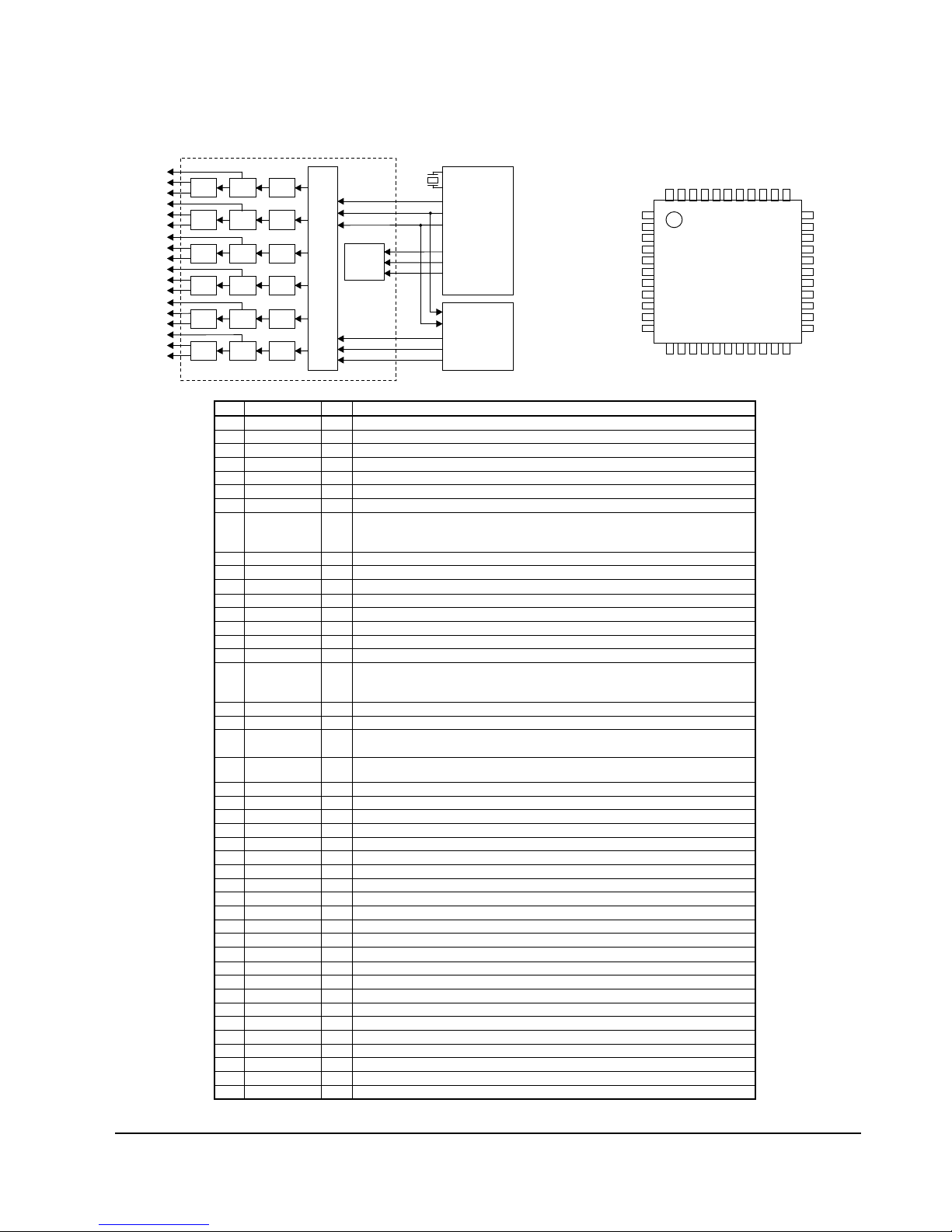
2-1-8 FIC1 (uPD780232 ; Front Micom)
80 7978 7776 75 74 7372 71 70 69 6867 66 65 64 63 62 61
21
1
2
3
4
5
6
7
8
9
10
11
12
13
14
15
16
17
18
19
20
V
LOAD
V
DD2
FIP20
FIP21
FIP22
FIP23
FIP24/P30
FIP25/P31
FIP26/P32
FIP27/P33
FIP28/P34
FIP29/P35
FIP30/P36
FIP31/P37
FIP32/P40
FIP33/P41
FIP34/P42
FIP35/P43
FIP36/P44
FIP37/P45
ANI1
ANI0
V
SS0
AV
DD
V
DD0
P64/FIP52
P63/FIP51
P62/FIP50
P61/FIP49
P60/FIP48
P57/FIP47
P56/FIP46
P55/FIP45
P54/FIP44
P53/FIP43
P52/FIP42
P51/FIP41
P50/FIP40
P47/FIP39
P46/FIP38
FIP0
FIP1
FIP2
FIP3
FIP4
FIP5
FIP6
FIP7
FIP8
FIP9
FIP10
FIP11
FIP12
FIP13
FIP14
FIP15
FIP16
FIP17
FIP18
FIP19
60
59
58
57
56
55
54
53
52
51
50
49
48
47
46
45
44
43
42
41
V
DD1
V
SS1
X1
X2
IC
RESET
P27/SCK1
P26/SI1
P25/SO1
P24/BUSY
P23
P22
P21/SO3
P20/SCK3
P00/INTP0
P01/INTP1
P02/TI
AV
SS
ANI3
ANI2
22 23 24 25 26 27 28 29 30 31 3233 34 35 36 37 3839 40
8-bit REMOTE
CONTROLLER
TIMER
(TM9)
8-bit TIMER
(TM80)
8-bit TIMER
(TM81)
A/D CONVERTER
(A/D1)
INTERRUPT
CONTROL
(INT)
SERIAL
INTERFACE
(2-WIRE MODE)
SERIAL
INTERFACE
(3-WIRE MODE)
WA TCHDOG TIMER
78K/0
CPU CORE
RAM
768 Bytes
ROM
16 Kbytes
PORT0
PORT2
PORT3
PORT4
PORT5
PORT6
P00 to P02
P20 to P27
P30 to P37
P40 to P47
P50 to P57
P60 to P64
SYSTEM
CONTROL
TI/P02
ANI0 to ANI3
AV
DD
AV
SS
INTP0/P00
BUSY/P24
SO1/P25
SO3/P21
SI1/P26
SCK1/P27
SCK3/P20
INTP1/P01
FIP0 to 23
FIP24/P30 to
FIP31/P37
FIP32/P40 to
FIP39/P47
FIP40/P50 to
FIP47/P57
FIP48/P60 to
FIP52/P64
FIP
CONTROLLER/
DRIVER
V
LOAD
V
DD2
RESET
X1
X2
V
DD0
,
V
DD1
V
SS0
,
V
SS1
V
PP
Reference Information
Samsung Electronics 2-11
Pin Name I/O Function
After Alternate
Reset Function
INTP0 Input Valid edge (rising edge, falling edge, or both rising and Input P00
INTP1
falling edges) can be specified.
P01
External interrupt request input.
TI Input 8-bit remote control timer (TM9) timer input Input P02
SCK3 I/O Serial interface serial clock I/O Input P20
SO3 Output Serial interface serial data output Input P21
BUSY Input Serial interface automatic transmit/receive busy signal output Input P24
SO1 Output Serial interface serial data output Input P25
SI1 Input Serial interface serial data input Input P26
SCK1 I/O Serial interface serial clock I/O Input P27
FIP0 to FIP23 Output FIP controller/driver high withstand voltage large current output Output
FIP24 to FIP31 P30 to P37
FIP32 to FIP39 P40 to P47
FIP40 to FIP47 Input P50 to P57
FIP48 to FIP52 P60 to P64
VLOAD FIP controller/driver pull-down resistor connection
RESET Input System reset input
X1 Input Crystal connection for main system clock oscillation
X2
ANI0 to ANI3 Input A/D converter analog input Input
AVDD A/D converter analog power supply/reference voltage input;
Keep the same potential with VDD1.
AVSS A/D converter ground potential; Keep the same potential with VSS1.
VDD0 Positive power supply for ports
VDD1
Positive power supply except for ports, analog, and FIP controller/driver
VDD2 Positive power supply for FIP controller/driver
VSS0 Ground potential for ports
VSS1 Ground potential except for ports and analog
IC Internally connected. Connect directly to V
SS1.
Non-port Pins
Pin Name I/O Function
After Alternate
Reset Function
P00 I/O Port 0. Input INTP0
3-bit I/O port.
P01
Input/output can be specified bit-wise.
INTP1
When used as an input port, an on-chip pull-up resistor can be connected
P02
by software.
TI
P20 I/O Port 2. Input SCK3
P21
8-bit I/O port.
SO3
P22, P23
Input/output can be specified bit-wise.
P24
When used as an input port, an on-chip pull-up resistor can be connected
BUSY
P25
by software.
SO1
P26 SI1
P27 SCK1
P30 to P37 Output Port 3. Output FIP24 to FIP31
P-ch open-drain 8-bit high withstand voltage I/O port.
A pull-down resistor can be incorporated bit-wise to VLOAD by mask option.
P40 to P47 Output Port 4. Output FIP32 to FIP39
P-ch open-drain 8-bit high withstand voltage output port.
A pull-down resistor can be incorporated bit-wise to VLOAD by mask option.
P50 to P57 I/O Port 5. Input FIP40 to FIP47
P-ch open-drain 8-bit high withstand voltage I/O port.
Input/output can be specified bit-wise.
A pull-down resistor can be incorporated bit-wise by mask option
(Connection to VLOAD or VSS0 can be specified bit-wise).
P60 to P64 I/O Port 6. Input FIP48 to FIP52
P-ch open-drain 5-bit high withstand voltage I/O port.
Input/output can be specified bit-wise.
A pull-down resistor can be incorporated bit-wise by mask option
(Connection to V
LOAD or VSS0 can be specified bit-wise).
Port Pins
Pin Name I/O Circuit Type I/O Recommended Connection of Unused Pins
P00/INTP0 8-C I/O Independently connect to VSS0 via a resistor.
P01/INTP1
P02/TI
P20/SCK3 Independently connect to VDD0 or VSS0 via a resistor.
P21/SO3
P22, P23
P24/BUSY
P25/SO1
P26/SI1
P27/SCK1
P30/FIP24 to P37/FIP31 14-F Output Leave open.
P40/FIP32 to P47/FIP39
P50/FIP40 to P57/FIP47 15-D I/O
P60/FIP48 to P64/FIP52
FIP0 to FIP23 14-F Output Leave open.
RESET 2 Input
ANI0 to ANI3 7 Independently connect to VSS0 via a resistor.
AVDD Connect to VDD1.
AVSS Connect to VSS1.
VLOAD
VPP Connect directly to VSS1.
Pin I/O Circuits and Recommended Connection of Unused Pins
Reference Information
2-12 Samsung Electronics
2-1-9 RIC1 (KS1461 ; RF Signal Processor)
RF
Equalizer
ALPC
D1
B1
A1
C1
DCD1
DDVD1
BDVD1
ADVD1
CDVD1
BCD1
CCD1
ACD1
F
E
MUX
TESEL(00H)
AUTO
OFSTCTL
TE3B
RFCT
&
MIRR
DPDVCC
LDODVD
ABCDN
12
17
14
15
16
25
22
70
55
100 98 94 92 89 8591 76848788 8293
GCA
TBAL(01H)
TEOFST(04H)
GAIN_TE3(02H )
+
21
18
19
20
FOKTH
DFCT_CP2
CC1
DGND
80 77787981
RFRP
71
ABCDI
ENV
90
CD1
+
+
+
+
RF SUM
&AGC
GAIN_EQ(02H)
ENVELOPE FOK DEFECT
24
AVCC
PDVD
PDLIMITRES
ABCD
SUB
RF
MUX
97 959699 86
VREFEQ
74
73
72
52
51
CLOCK
DATA
VREFDPD
toDPD
BLO CK
to RF EQ
TUNING BLOCK
13
23
FOFST
LDOCD
PDCD
53
54
DVCC
75
BCA
FAULTOUT
56
83
AGND
STB
DPDGND
MUX
BCAI
DPDEQ2
DPDEQ1
DFCT2
TE3OFST
ANALOG
VC AMP
VREFA
DFCT_CP1
VREFLP_BGI
CC2
DPD
VC AMP
TEN
TE
DFCT1
FE
PLLCTL
TE1RES
MIRR
DPDMUTE
OSC
FOKB
-
+
FOFST
AB CD
SUM
+
FE
OFSTHOLD
FEN
DFCTTH2
DFCTTH1
ENVP
ENVB
RESET
BCAO
AGC_D ET
RFAGCO
AGCLEVEL
AGCI
EQVCC
RFEQO
PLLF
BCATH
EQF
RDPF
VZOCTL
AGCC
RFCT
EQGND
CP1
MIRRI
RFRPN
CP2
CB2
RFRP
AGCP
AGCB
CB1
MROFST
EQIN
RREFDLY
VREF
GENERATOR
RREFBF
RREF
RREFEQ
EQ VC
AMP
58
60
59
57
65
62
63
61
64
68
67
66
69
S/ I F
BLOCK
CD1
S12
DVD1
DVD2
LDONB
FLT_CTL
CDRSEL
TESEL
AGC HOLD
TBAL
GAIN_TE3
ENV_ SE L
DVCTL_SEL
DPD_MUTE
GAIN_EQ
GAIN_FE
GAIN_ABCD
TE_OFST
FE_OFST
ABCD_ OFST
DELAY_CD
DELAY_AB
PDL IM I T
ga_RFSUM
HOLD_CTL
ga_PLLDP
ga_PLLDN
BCA
BLOCK
BCA
MUX
EQIN
-+
AGC-HOLD(00H)
ENV_SEL(02H)
LDONB(00H)
COM
DPDEQ 1
DPDEQ 2
COM
DELAY
DELAY_AB(07H)
DELAY_CD (07H)
PLLCTL
TEOFST(04H)
PD,LPF
PD_LIMIT(0 8H)
DELAY _SEL(00H)
PLL CTL
TBAL( 01H)
DELAY_SEL(00H)
PLL CTL
FAULTOUT
TE1R ES
TE1_LIMIT
PDLIMITR ES
GA_PLLDN(09 H)
GA_PLLDP(09 H )
+
+
EQ
+
+
EQ
CDRSEL(00H)
D
B
A
C
RF
MUX
ACD
CCD
DCD
BCD
6
7
8
ADVD
CDVD
DDVD
BDVD
2
3
4
5
1
D
D
D
D
MUX3
DVCTL_SE L(02H)
GCA
GCA
ga_RFSUM(08H)
HOL D_CTL( 0 8 H)
DPDMUTE
DPD_MUTE(02H)
SEOFHOL D
FL T_CT L(00 H)
CAL_ENDB(02H)
CDRSEL(00H)
OFSTHOLD
GAIN_FE(03H)
OFSTHOLD
+
+
+
-
CDRSEL(00H)
OFSTHOLD
S12
GAIN_ABCD(00H )
ABCD _OFST(06 H)
FE_OFST(05 H)
9
10
11
Ab normal waveform
Detection circuit
GCA
31 42 43 4644 5026 27 40 41 47 4839 453428 32 3329 30 36 37 3835 49
EQG
Reference Information
Samsung Electronics 2-13
Pin
No.
Pin Name I/O Description Related Block
Related
Part
1 ACD I Optical main beam A, AC Coupling input terminals for CD of RF
block
PRE AMP P/U
2 BCD I Optical main beam B, AC Coupling input terminals for CD of RF
block
PRE AMP P/U
3 CCD I Optical main beam C, AC Coupling input terminals for CD of RF
block
PRE AMP P/U
4 DCD I Optical main beam D, AC Coupling input terminals for CD of RF
block
PRE AMP P/U
5 ADVD I Optical main beam A, AC Coupling input terminals for DVD of RF
block
PRE AMP P/U
6 BDVD I Optical main beam B, AC Coupling input terminals for DVD of RF
block
PRE AMP P/U
7 CDVD I Optical main beam C, AC Coupling input terminals for DVD of RF
block
PRE AMP P/U
8 DDVD I Optical main beam D, AC Coupling input terminals for DVD of RF
block
PRE AMP P/U
9 RREFBF - RF AMP I/O buffer bias resistance connection terminal RF AMP 10 RREFEQ - RF EQ BIAS resistance connection terminal RF EQ 11 RREF - Analog Block bias resistance connection terminal ANALOG 12 VREFEQ - CAP connection terminal for RF EQ Center voltage EQ VC AMP 13 E I CD Optical sub beam E input terminal for Servos TE 3B P/U
14 F I CD Optical sub beam F input terminal for Servos TE 3B P/U
15 ADVD1 I Optical main beam A input terminal for DVD of Servo block SERVO AMP P/U
16 BDVD1 I Optical main beam B input terminal for DVD of Servo block SERVO AMP P/U
17 CDVD1 I Optical main beam C input terminal for DVD of Servo block SERVO AMP P/U
18 DDVD1 I Optical main beam D input terminal for DVD of Servo block SERVO AMP P/U
19 ACD1 I Optical main beam A input terminal for CD of Servo block SERVO AMP P/U
20 BCD1 I Optical main beam B input terminal for CD of Servo block SERVO AMP P/U
21 CCD1 I Optical main beam C input terminal for CD of Servo block SERVO AMP P/U
22 DCD1 I Optical main beam D input terminal for CD of Servo block SERVO AMP P/U
23 AVCC P Power voltage input terminal for Analog Part ANALOG 24 VREFA I/O CAP connection terminal for Analog Part center voltage
Uses an external block
ANA VC AMP SERVO
25 FOFST - CAP connection terminal (open) for Focus Auto Offsets FE AMP 26 OFSTHOLD I On/Off terminal for Auto Offset Block.
(L: Auto Offset Adjustments, H: Serial Offset Adjustments)
OFSTCTL MICOM
27 VREFLP_BGI I Band gap voltage input block for ALPC ALPC 28 LDODVD O
Optical Laser Diodes operation voltage output terminal for DVD
ALPC P/U
29 PDDVD I
Optical Laser Monitor Diode voltage input terminal for DVD
ALPC P/U
30 LDOCD O
Optical Laser Diode operating voltage output terminal for CD
ALPC P/U
31 PDCD I
Optical Laser Monitor Diode voltage input terminal for CD
ALPC P/U
32 AGND P
Power GND terminal for Analog Part
ANALOG -
33 FE O
FE AMP output terminal
FE AMP DSSP
34 FEN I
Input terminal for selecting FE AMP Gain
FE AMP -
35 TEN I
Input terminal for selecting TE AMP Gain
TE AMP -
36 TE O
TE AMP output terminal
TE AMP DSSP
37 PDLIMTRES -
Bias resistance terminal for PDLIMIT
DPD -
38 ABCDN I
ABCD AMP for selecting Gain (
- ) input terminal
ABCD AMP -
39 ABCD O
ABCD AMP output terminal
ABCD AMP -
40 ABCDI I
ABCD AC Coupling input terminal for servo monitor
SERVO MONIT -
41 ENVP -
CAP connection terminal for selecting the RC value of Peak Hold
for detecting RF Envelopes
RF ENV -
42 ENVB -
CAP connection terminal for selecting the RC value of Bottom
Hold for detecting RF Envelopes
RF ENV -
43 ENV O
RF Envelope Detect Output terminal
RF ENV DSSP
44 DGND P
Power GND input terminal for digital circuits
DIGITAL -
45 FOKTH I
Focus OK comparating level input terminal
FOKB -
46 FOKB O
Focus OK comparator output terminal (L: Focus OK)
FOKB DSSP
47 DFCT_CP1 -
Connection terminal for RC value of Peak Hold, for selecting the
maximum time for Servo signal
DFCT -
48 DFCT_CP2 -
Connection terminal for RC value of Peak Hold, for selecting the
minimum defect time for PLL
DFCT -
49 CC1 O
Peak Hold Output terminal for selecting the minimum Defect time
for Defect
DFCT -
50 CC2 I
Peak Hold AC Coupling Input terminal for Defect
DFCT -
51 DVCC P
Power voltage input terminal for digital circuit
DIGITAL -
52 DFCTTH2 -
Resistance connection terminal for selecting the Defect Comparating Level for PLL
DEFECT -
53 DFCTTH1 -
Resistance connection terminal for selecting the Defect Comparating Level for Servo
DEFECT -
54 DFCT1 O
Defect output terminal for Servo
DEFECT DSSP
55 DFCT2 O
Defect output terminal for PLL
DEFECT PLL
56 DPDVCC P
Power voltage input terminal for DPD TE
DPD -
57 MIRR O
Mirror output terminal
MIRR DSSP
58 BCA O
BCA output terminal
BCA DSP
59 TE3OFST -
Cap connection terminal (open) for 3B TE Offset
3B TE AMP -
60 DPDEQ1 O
DPD EQ (A+C) output terminal
DPD -
61 DPDEQ2 O
DPD EQ (B+D) output terminal
DPD -
62 FAULTOUT O
DPD abnormal wave form output terminal (monitor)
DPD -
63 DPDMUTE I
DPD TE MUTE control terminal (H: Mute)
DPD MICOM
64 PLLCTL I
DPD TE PLL variable input terminal
DPD SERVO
65 TE1RES I
DPD TE PLL variable bias resistance
DPD -
66 DPDGND P
Power GND input terminal for DPD TE
DPD -
67 VREFDPD O
CAP connection terminal for DPD TE center voltage
DPD VC AMP -
68 RREFDLY -
Bias resistance connection terminal for Delay Block
Delay Block -
69 DATA I
Data input terminal
Serial Interface MICOM
70 CLOCK I
Clock input terminal
Serial Interface MICOM
71 STB I
Data Enable input terminal
Serial Interface MICOM
72 OSC
Input terminal for RC value of OSC, for Auto Offset Block
Auto OFSTCTL -
73 RESET I
Reset input terminal (L: Reset) for Auto Offset Block
Auto OFSTCTL MICOM
74 BCAI I
BCA Filter1
BCA -
75 BCAO O
BCA Filter2
BCA -
76 RFCT O
RF Ripple Center voltage output terminal for Mirror
MIRROR DSSP
77 CB2 -
CAP connection terminal of RC value of Bottom Hold, for RFCT
generation
MIRROR -
78 CP2 -
CAP connection terminal of RC value of Peak Hold, for RFCT generation
MIRROR -
79 RFRP O
RF Ripple Amp output terminal for Mirror
MIRROR DSSP
80 RFRPN I
Input terminal for selecting RFRP Amp gain
MIRROR -
81 MROFST I
RF Ripple Offset control terminal for Mirror
MRROR -
82 CB1 -
RC connection terminal of RC value of Bottom Hold, for RFRP
generation
MRROR -
83 CP1 -
RC connection terminal of RC value of Peak Hold, for RFRP generation
MRROR -
84 MIRRI I
Input terminal for MIRR signal generation
MRROR -
85 EQVCC P
Power voltage input signal for RF EQ
RF EQ -
86 RFEQ0 0
RF EQ output terminal
RF EQ PLL
87 BCATH I
BCA Comparating Level control terminal
BCA DSP
88 EQIN I
RFAGCO input terminal for RF EQ
RFEQ,RFENV DSSP
89 RFAGCO O
RF AGC AMP output terminal
RF AGC -
90 AGCC -
CAP connection terminal for time constant of AGC
RF AGC -
91 AGCI I
AGC voltage input terminal while in AGC hold
RF AGC -
Pin
No.
Pin Name I/O Description Related Block
Related
Part
92 EQGND P
Power GND input terminal for RF EQ
RF EQ -
93 AGCLEVEL I
AGC Level control voltage input terminal (3.5 V) while in AGC hold
off
RF AGC -
94 AGCB -
RC connection terminal for RC value of Bottom Hold, for RF AGC
RF AGC -
95 AGCP -
RC connection terminal for RC value of Peak Hold, for RF AGC
RF AGC -
96 RDPF -
Bias resistance connection terminal for selecting RF EQ frequency
RF EQ -
97 EQG I
RF EQ Boost Gain control voltage input terminal
RF EQ DSSP
98 EQF I
RF EQ Peak Frequency control voltage input terminal
RF EQ DSSP
99 PLLF I
Wide-band PLL compatible RF EQ Peak Frequency Control terminal
RF EQ DSSP
100 VZOCTL I
RF EQ zero control terminal
RF EQ DSSP
Related
Reference Information
2-14 Samsung Electronics
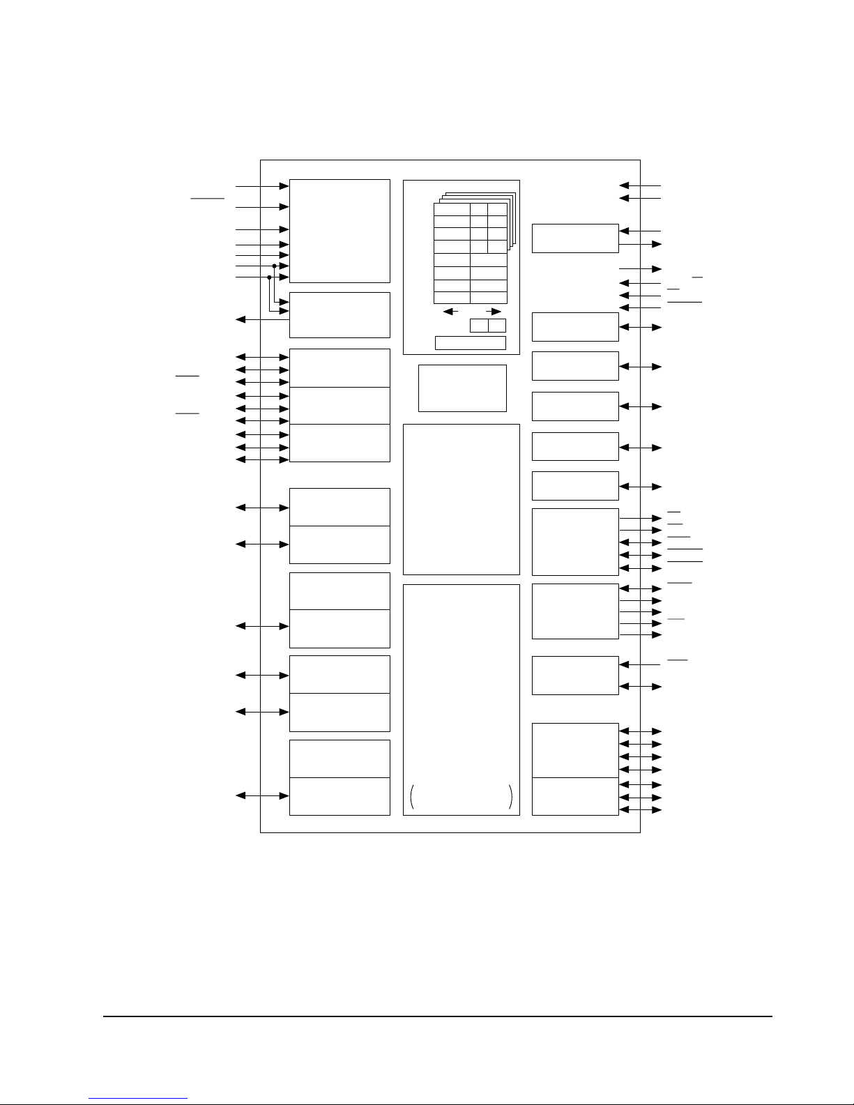
2-1-10 SIC1 (KS1452 ; Servo Processor)
XI
XO
TIMING
GENER ATOR
TR ACK COUNTER
VREF
FOD
TRD
SL D
SPD
FBAL
TBAL
A/D
CONVERTER
BLOC K
ENV
SME
TE
FE
D/A
CONVERTER
BLOC K
COUT
FLKB
TLKB
SSTOP/PS0
PS1
LOCK
SMON
MIRR
FOKB
DFCT
I/O INTERFACE BLOC K
DAB
CSB
MDAT A[ 7:0]
MWRB
SENSE
SYSCON
INTERFACE
BLOCK
ROM
DSP CORE
FOR
DIGITAL SERVO
PL CK
RVCO
VCTRL
EQC TL
WIDE CAPTURE
RANGE PLL
LDONB
PSB
RSTB
TEST
TZCA
MRDB
EFM ASYMMETRY
RFI
ASYCD
XOUT
TILTI
TILTO
EFM
EFMR TD
RPD
PLLLOCK
MDOUT[3:0]
DIRC
ASYDVD
EFMI
DVCTL
MAGIC0
INT0_224
PL LHD
RFD
PHI1
EFMOA
FDCTL
TZCO
Reference Information
Samsung Electronics 2-15
41 PVDD P PLL logic block VDD power supply pin
42 PLCK O PLCK
43 PLLLOCK O Frequency lock detect output (H: lock, L: unlock)
44 EFMRTD O Latched EFM output signal
45 PVSS P PLL logic block VSS power supply pin
46 RVCO I Resistor pin for VCO gain
47 RFD I Gain adjust resister for frequency detector
48 RPD I Gain adjust resister for phase detector
49 VCTL I control voltage for VCO
50 MAGIC0 I Input for controlling hysteresis of the FD output (for testing)
51 EFMOA I EFM offset adjustment pin
52 TZCO O Tracking zero cross output pin
53 SVDD P Servo CPU VDD power supply pin
54 EQCTL O EQ control signal
55 EFMI I EFM signal for test
56 EFMO O EFM signal
57 LPFDVD I Asymmetric input signal for DVD
58 LPFCD I Asymmetric input signal for CD
59 RFI I Rf input signal
60 SVSS P Servo CPU VSS power supply pin
61 AVSS P Analog block VSS power supply pin
62 SME I Spindle error input pin
63 VREF I Reference voltage input pin
64 TE I Tracking error signal input pin
65 FE I Focus error signal input pin
66 ENV I RF envelope input pin
No Name I/O Description
67 TILTI I TILT in (reserved)
68 AVDD P Analog block VDD power supply pin
69 TILTO O TILT out (reserved)
70 DVCTL O Depth variation control signal output pin
71 TBAL O Tracking balance signal output pin
72 FBAL O Focus balance signal output pin
73 SLD O Sled motor drive signal output pin
74 SPD O Spindle motor drive signal output pin
75 FOD O Focus actuator drive signal output pin
76 TRD O Tracking actuator drive signal output pin
77 TZCA I TE signal for tracking zero cross input pin
78 MDOUT0 O Mode data0 out controlled by micom
79 MDOUT1 O Mode data1 out controlled by micom
80 MDOUT2 O Mode data2 out controlled by micom
No Name I/O Description
1 MDOUT3 O Mode data3 out controlled by micom
2 SSTOP/PS0PS1 I Limit switch/sled position sensor input pin0
3 PS1 I Sled motor position sensor input pin1
4 TEST I Test pin (L: normal H: test)
5 COUT O Counter clock
6 FLKB O Focus servo lock signal output pin
7 TLKB O Tracking servo lock signal output pin
8 PSB I 0: 1 Bit, 1: 8 Bit
9 RSTB I System reset signal input pin
10 CSB I MICOM chip select pin
11 DAB I MICOM data/addrs select pin
12 MWRB I MICOM write clock signal input pin
13 MRDB I MICOM read clock signal input pin
14 MDATA0 I/O MICOM data pin0
15 MDATA1 I/O MICOM data pin1
16 MDATA2 I/O MICOM data pin2
17 MDATA3 I/O MICOM data pin3
18 MDATA4 I/O MICOM data pin4
19 MDATA5 I/O MICOM data pin5
20 MDATA6 I/O MICOM data pin6
21 MDATA7 I/O MICOM data pin7
22 SENSE O Internal status monitor pin
23 DVDD P Servo logic & ROM VDD power supply pin
24 XI I System clock signal input pin
25 XO O System clock signal output pin
26 XOUT O Clock out (33.9688MHz) to DSP
27 DVSS P Servo logic & ROM VSS power supply pin
28 SQCK O Clock output pin for subcode data read
29 SQSI I Subcode data input pin
30 SCOR I Timing detection input pin for subcode data read
31 SMON I Motor ON signal input pin
32 LOCK I Lock signal input pin
33 DIRC I
Direct jump control (for 1 track jump)
34 FOKB I Focus OK signal input pin
35 FDCTL I PLL frequency detect control input pin
36 LDONB O Laser diode ON signal output pin
37 DFCT I Defect detection signal input pin
38 MIRR I Mirror signal input pin
39 PLLHD I PLL hold signal from micom
40 INT0_224 O Servo interrupt monitor pin
Reference Information
2-16 Samsung Electronics
2-1-11 SIC4 (KA3017 ; Motor & Actuator Driver)
123654789101112
13
14
15
16
17
18
19
20
21
22
23
24
25 26 27 28 29 30 31 32 33 34 35 36
37
38
40
39
42
41
43
44
45
46
47
48
Hall bias
FG
Comparator
Absolute
Values
TSD
Detector
Direction
Detector
+
-
Hall amp matrix
Direction select
+
-
-
+
+
-
+
-
+
-
+
-
+
-
+
-
+
-
+
-
Power
Save
Short vrake
+
-
Lower
Distributor
Upper
Distributor
MUTE
MUTE
MUTE
2P
2P
2P
2P
2P
2P
2P
2P
2P
10k
10k
10k
10k
PWRGND
A3
A2
A1
OPIN +
OPIN
-
OPOUT
VCC1
AVM12
DI4
DI3
DI2
FIN (GND)
FIN (GND)
H3+
H3
-
H2+
H2
-
H1+
H1
-
BTLSGND
BIAS
AVM4
MUTE12
MUTE3
MUTE4
DI1
DO1
-
DO1 +
DO2
-
DO2 +
BTLPGND1
BTLPGND2
DO3
DO3 +
AVM3
DO4
-
DO4 +
FIN (GND)
SB
DIR
SS
CS1
VM
SIGGND
PC1
VCC2
EC
ECR
FG
VH
FIN (GND)
Reference Information
Samsung Electronics 2-17
No. Symbol I/O Description
1 VH I HALL BIAS
2 FG O FG SIGNAL OUTPUT
3 ECR I TORQUE CONTROL REFERENCE
4 EC I TORQUE CONTROL SIGNAL
5 VCC2 — SUPPLY VOLTAGE
6 PC1 — PHASE COMPENSATION CAPACITOR
7 SIGGND — SIGNAL GROUND
8VM— MOTOR SUPPLY VOLTAGE
9 CS1 I CURRENT SENSOR
10 S/S I START/STOP
11 DIR O 3-PHASE ROTATIONAL DIRECTION OUTPUT
12 SB I SHORT BRAKE
13 PWRGND — POWER GROUND
14 A3 O 3-PHASE OUTPUT 3
15 A2 O 3-PHASE OUTPUT 2
16 A1 O 3-PHASE OUTPUT 1
17 OPIN+ I OP AMP INPUT (+)
18 OPIN- I OP AMP INPUT (-)
19 OPOUT O OP AMP OUTPUT
20 VCC1 — SUPPLY VOLTAGE
21 AVM12 — BTL CH-1, 2 MOTOR SUPPLY VOLTAGE
22 DI4 I BTL DRIVE INPUT 4
23 DI3 I BTL DRIVE INPUT 3
24 DI2 I BTL DRIVE INPUT 2
25 DI1 I BTL DRIVE INPUT 1
26 DO1- O BTL DRIVE 1 OUTPUT (-)
27 DO1+ O BTL DRIVE 1 OUTPUT (+)
28 DO2- O BTL DRIVE 2 OUTPUT (-)
29 DO2+ O BTL DRIVE 2 OUTPUT (+)
30 BTLPGND1 — BTL POWER GROUND 1
31 BTLPGND2 — BTL POWER GROUND 2
32 DO3- O BTL DRIVE 3 OUTPUT (-)
33 DO3+ O
BTL DRIVE 3 OUTPUT (+)
34 AVM3 — BTL CH3 MOTOR SUPPLY VOLTAGE
35 DO4- O BTL DRIVE 4 OUTPUT (-)
36 DO4+ O BTL DRIVE 4 OUTPUT (+)
37 MUTE4 I BTL DRIVE MUTE CH 4
38 MUTE3 I BTL DRIVE MUTE CH 3
39 MUTE12 I BTL DRIVE MUTE CH 1, 2
40 AVM4 — BTL CH 4 MOTOR SUPPLY VOLTAGE
41 BIAS — BTL BIAS VOLTAGE
42 BTLSGND — BTL DRIVE SIGNAL GROUND
43 H1- I HALL1(-) INPUT
44 H1+ I HALL1(+) INPUT
45 H2- I HALL2(-) INPUT
46 H2+ I HALL2(+) INPUT
47 H3- I HALL3(-) INPUT
48 H3+ I
HALL3(+) INPUT
Reference Information
2-18 Samsung Electronics
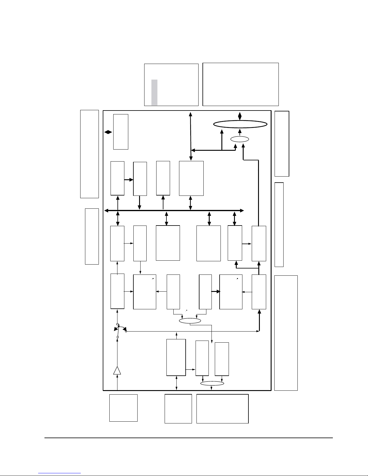
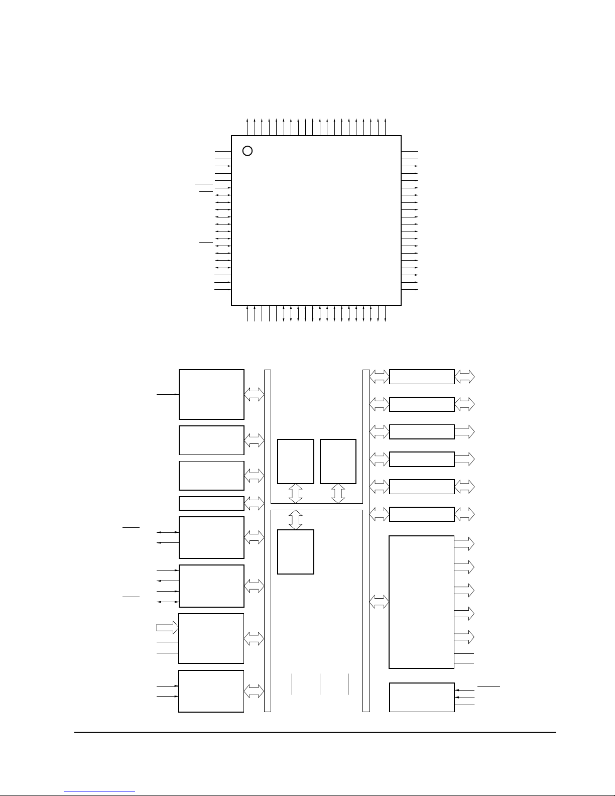
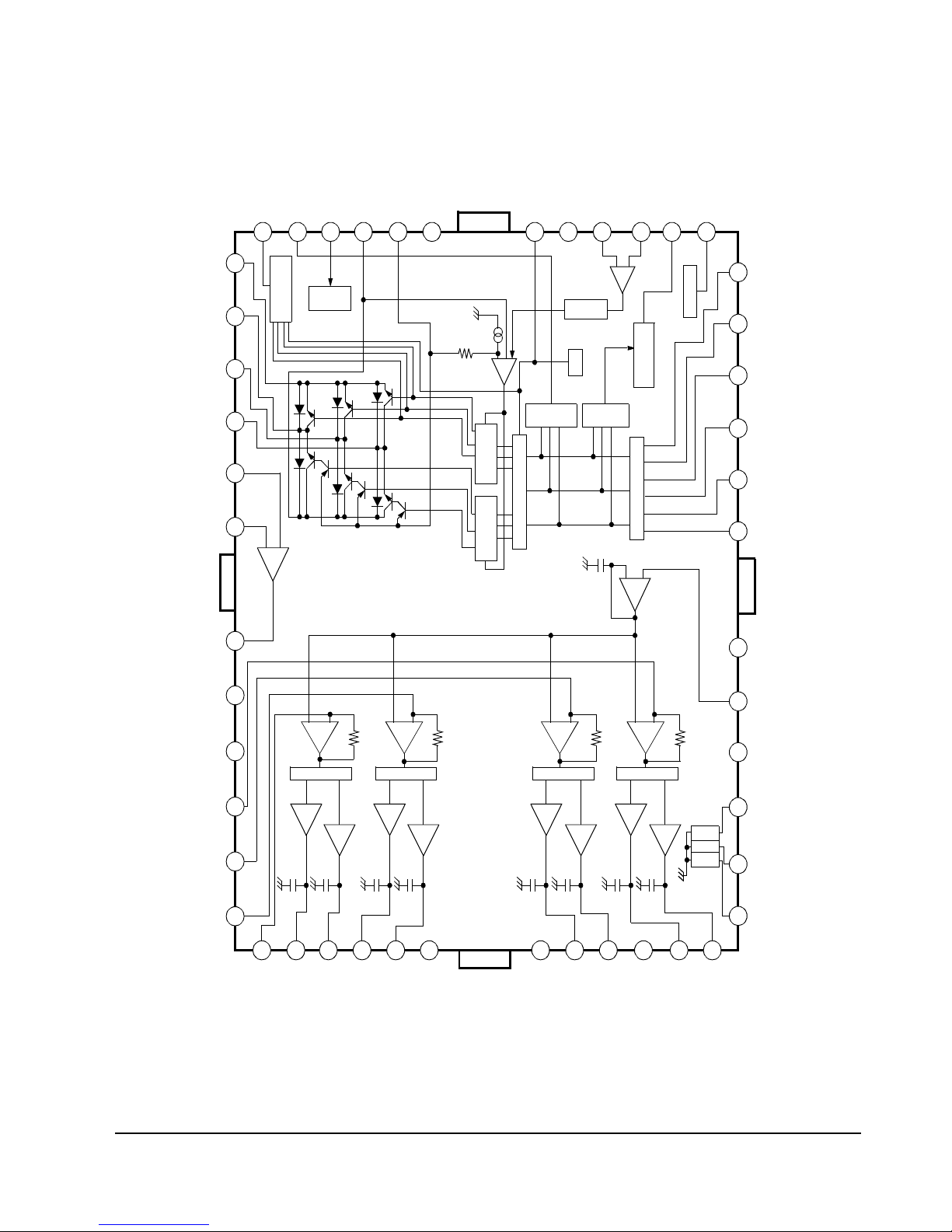
2-1-12 ZIC1 (ZIVA 4.1 ; A/V Decoder)
Digital Audio Input
SDRAM
Interface
Audio
DSP
Digital
Audio
Interface
Program
Stream
Decoder
Host
Interface
Audio
Interface
DVD/CD
Interface
MPEG Video
Decoder
Subpicture
Decoder
OSD
Decoder
CD-DA and LPCM
Decoder
Dolby Digital Audio
Decoder
MPEG Audio
Decoder
Memory
Controller
Host
Interface
Control Logic
SecureView
CSS
Descrambling
Bus Key
Authentication
(optional)
Video
Mixer
Video
Out
Digital
Video
Encoder
Reference Information
Samsung Electronics 2-19
Pin No . Pin Name I/O Volta g e I/O Ty p e
1RD
3.3V I
2R/W
3.3V I
3 VDD_3.3 3.3V
4 WAIT
3.3V O, OD, PU
5RESET3.3V I
6 VSS GROUND
7 VDD_3.3 3.3V
8INT
3.3V O, OD, PU
9 NC No Connect O
10 NC No Connect O
11 NC No Connect O
12 NC No Connect O
13 VDD_2.5 2.5V
14 VSS GROUND
15 NC No Connect O
16 NC No Connect O
17 NC No Connect O
18 NC No Connect O
19 VSS GROUND
20 VDD_3.3 3.3V
21 VDATA0 3.3V O
22 VDATA1 3.3V O
23 VDATA2 3.3V O
24 VDAT
A3 3.3V O
25 VDATA4 3.3V O
26 VDATA5 3.3V O
27 VDATA6 3.3V O
28 VDATA7 3.3V O
29 VSYNC
3.3V I/O
30 HSYNC
3.3V I/O
31 VSS GROUND
32 VDD_3.3 3.3V
33 RESERVED 3.3V I
34 RESERVED 3.3V I
35 RESERVED 3.3V I
36 VDD_2.5 2.5V
37 VSS GROUND
38 RESERVED 3.3V I
39 RESERVED 3.3V I
40 RESERVED 3.3V I
41 RESERVED 3.3V I
42 RESERVED 3.3V I
43 PIO0 3.3V I/O
44 VSS GROUND
45 VDD_3.3 3.3V
46 PIO1 3.3V I/O
47 PIO2 3.3V I/O
48 PIO3 3.3V I/O
49 PIO4 3.3V I/O
50 PIO5 3.3V I/O
51 PIO6 3.3V I/O
52 PIO7 3.3V I/O
53 MDATA0 3.3V I/O
54 MDATA1 3.3V I/O
55 VDD_3.3 3.3V
56 VSS GROUND
57 MDATA2 3.3V I/O
58 MDATA3 3.3V I/O
59 MDATA4 3.3V I/O
60 MDATA5 3.3V I/O
61 MDATA6 3.3V I/O
62 MDATA7 3.3V I/O
63 MDAT A 15 3.3V I/O
64 VDD_3.3 3.3V I/O
65 VSS GROUND I/O
66 MDAT A 14 3.3V I/O
67 VDD_2.5 2.5V
68 VSS GROUND
69 MDAT A 13 3.3V I/O
70 MDAT A 12 3.3V I/O
71 MDAT A 11 3.3V I/O
72 MDAT A 10 3.3V I/O
73 MDATA9 3.3V I/O
74 VDD_3.3 3.3V
75 VSS GROUND
76 MDATA8 3.3V I/O
77 LDQM 3.3V O
78 SD-CLK 3.3V O
79 CLKSEL 3.3V I
80 MADDR9 3.3V O
81 MADDR8 3.3V O
82 VDD_3.3 3.3V
83 VSS GROUND
84 MADDR7 3.3V O
85 MADDR6 3.3V O
86 MADDR5 3.3V O
87 VDD_2.5 2.5V
88 VSS GROUND
89 MADDR4 3.3V O
90 MWE
3.3V O
91 SD-CAS
3.3V O
92 VDD_3.3 3.3V
93 VSS GROUND
94 SD-RAS
3.3V O
95 SD-CS0
3.3V O
96 SD-CS1
/MADDR11 3.3V O
Pin No. Pin Name I/O Voltage I/O Type
97 SD-BS
3.3V O
98 MADDR10 3.3V O
99 MADDR0 3.3V O
100 VDD_3.3 3.3V
101 VSS GROUND
102 MADDR1 3.3V O
103 MADDR2 3.3V O
104 MADDR3 3.3V O
105 RESERVED ANALOG GND
106 NC No connect O
107 NC No connect O
108 RESERVED 3.3V I
109 NC No connect O
110 RESERVED 3.3V I
111 RESERVED 3.3V ANALOG
112 RESERVED 3.3V I
113 DAI-LRCK 3.3V I/O
114 DAI-BCK 3.3V I/O
115 VDD_3.3 3.3V
116 VSS GROUND
117 DAI- DATA 3.3V I/O
118 DA-DATA3 3.3V O
119 DA-DATA2 3.3V O
120 DA-DATA1 3.3V O
121 DA-DATA0 3.3V O
122 DA-LRCK 3.3V O
123 VDD_3.3 3.3V
124 VSS GROUND
125 DA-XCK 3.3V I/O
126 DA-BCK 3.3V O
127 DA-IEC 3.3V O
128 VDD_2.5 2.5V
129 VSS GROUND
130 NC No Connect O
131 VSS_DAC ANALOG GND
132 VSS_VIDEO ANALOG GND
133 CVBS + sync 3.3V ANALOG O
134 VDD_DAC 3.3V ANALOG O
135 VDD_VIDEO 3.3V ANALOG
136 NC No Connect O
137 VSS_DAC ANALOG GND
138 VSS_VIDEO ANALOG GND
139 CVBS/G/Y 3.3V ANALOG O
140 VDD_DAC 3.3V ANALOG
141 VDD_VIDEO 3.3V ANALOG
142 NC No Connect O
143 VSS_DAC ANALOG GND
Pin No . Pin Name I/O Volta g e I/O Ty p e
144 VSS_VIDEO ANALOG GND
145 Y/B/U 3.3V ANALOG O
146 VDD_DAC 3.3V ANALOG
147 VDD_VIDEO 3.3V ANALOG
148 NC No Connect O
149 VSS_DAC ANALOG GND
150 VSS_VIDEO ANALOG GND
151 C/R/V 3.3V ANALOG O
152 VDD_DAC 3.3V ANALOG
153 VDD_VIDEO 3.3V ANALOG
154 VSS_RREF ANALOG GND
155 RREF 3.3V ANALOG O
156 VDD_RREF 3.3V ANALOG
157 A_VSS GROUND
158 SYSCLK 3.3V I
159 VCLK 3.3V I
160 A_VDD 3.3V ANALOG
161 DVD-DATA0/CD-DA TA 3.3V I
162 DVD-DATA1/CD-LRCK 3.3V I
163 DVD-DATA2/CD-BCK 3.3V I
164 DVD-DATA3/CD-C2P0 3.3V I
165 DVD-DATA4/CDG-SDATA 3.3V I
166 VSS GROUND
167 VDD_3.3 3.3V
168 DVD-DATA5/CDG-VFSY 3.3V I
169 DVD-DATA6/CDG-S0S1 3.3V I
170 DVD-DATA7/CDG-SCLK 3.3V I
171 VDACK 3.3V I
172 VREQUEST 3.3V O
173 VSTROBE 3.3V I
174 ERROR 3.3V I
175 VDD_3.3 3.3V
176 RESERVED GROUND
177 VDD_3.3 3.3V
178 VSS GROUND
179 NC No connect O
180 NC No connect O
181 NC No connect O
182 HADDR0 3.3V I
183 HADDR1 3.3V I
184 HADDR2 3.3V I
185 RESERVED 3.3V I
186 RESERVED 3.3V I
187 RESERVED 3.3V I
188 VSS GROUND
189 VDD_2.5 2.5V
190 RESERVED 3.3V I
Pin No. Pin Name I/O Voltage I/O Type
Reference Information
2-20 Samsung Electronics
191 VSS GROUND
192 VDD_3.3 3.3V
193 RESERVED 3.3V I
194 RESERVED 3.3V I
195 RESERVED 3.3V I
196 RESERVED 3.3V I
197 HDA TA7 3.3V I/O
198 VSS GROUND
Pin No . Pin Name I/O Volta g e I/O Ty p e
199 HDATA6 3.3V I/O
200 HDATA5 3.3V I/O
201 HDATA4 3.3V I/O
202 HDATA3 3.3V I/O
203 HDATA2 3.3V I/O
204 VDD_3.3 3.3V
205 VSS 3.3V
206 HDATA1 3.3V I/O
207 HDATA0 3.3V I/O
208 CS
3.3V I
Pin No. Pin Name I/O Voltage I/O Type
Reference Information
Samsung Electronics 2-21
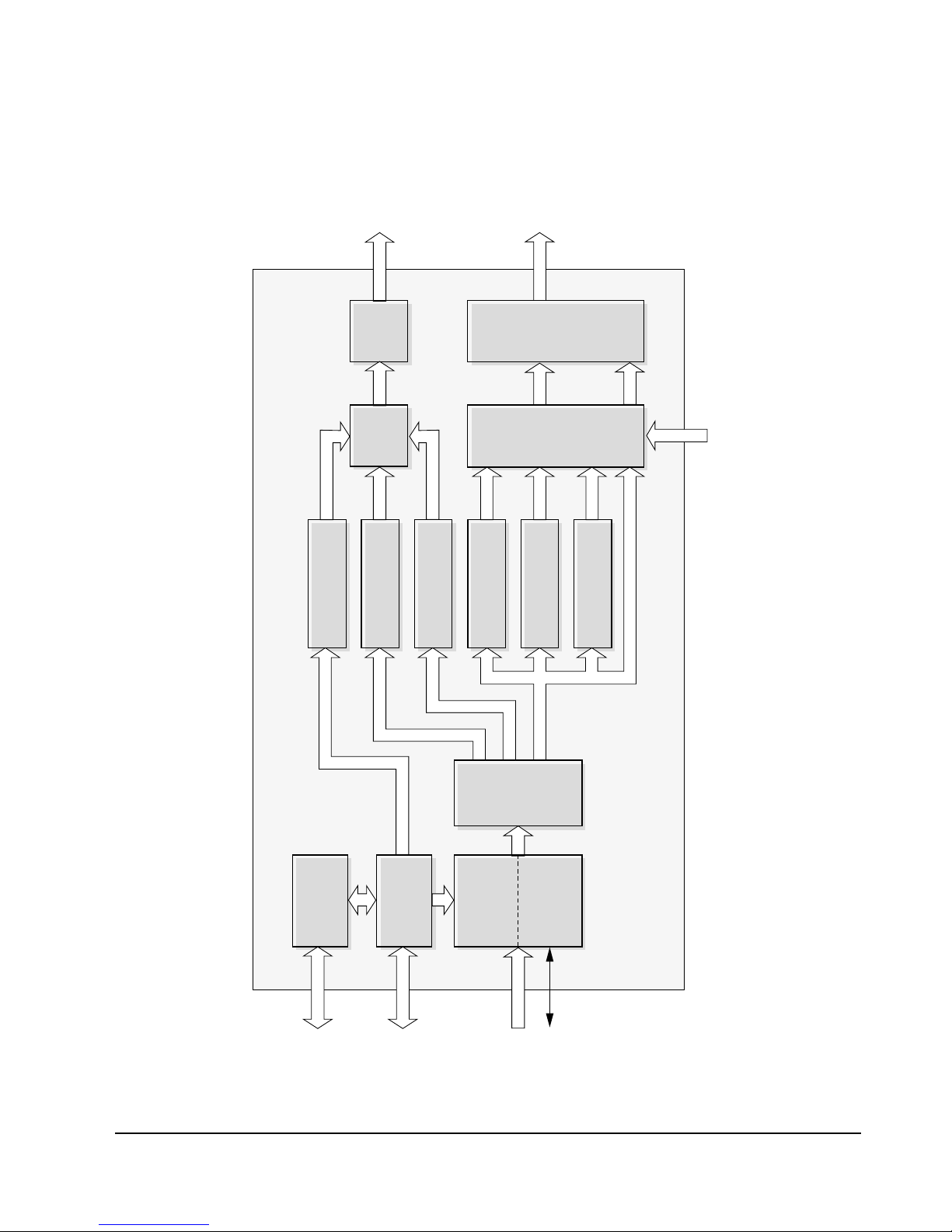
2-1-13 ZIC2/ZIC3 (KM416S1120D ; CMOS 16M SDRAM)
Bank Select
Data Input Register
512K x 16
512K x 16
Sense AMP
Output BufferI/O Control
Column Decoder
Latency & Burst Length
Programming Register
Address Register
Row Buffer
Refresh Counter
Row Decoder Col. Buffer
LRAS
LCBR
LCKE
LRAS LCBR LWE LDQM
CLK CKE CS
RAS CAS WE L(U)DQM
LWE
LDQM
DQi
CLK
ADD
LCAS LWCBR
Timing Register
VDD
DQ0
DQ1
V
SSQ
DQ2
DQ3
V
DDQ
DQ4
DQ5
V
SSQ
DQ6
DQ7
V
DDQ
LDQM
WE
CAS
RAS
CS
BA
A10/AP
A0
A1
A2
A3
V
DD
1
2
3
4
5
6
7
8
9
10
11
12
13
14
15
16
17
18
19
20
21
22
23
24
25
50
49
48
47
46
45
44
43
42
41
40
39
38
37
36
35
34
33
32
31
30
29
28
27
26
VSS
DQ15
DQ14
V
SSQ
DQ13
DQ12
V
DDQ
DQ11
DQ10
V
SSQ
DQ9
DQ8
V
DDQ
N.C/RFU
UDQM
CLK
CKE
N.C
A9
A8
A7
A6
A5
A4
V
SS
Pin Name Input Function
CLK System Clock Active on the positive going edge to sample all inputs.
CS
Chip Select
Disables or enables device operation by masking or enabling all inputs except
CLK, CKE and L(U)DQM
CKE Clock Enable
Masks system clock to freeze operation from the next clock cycle.
CKE should be enabled at least one cycle prior to new command.
Disable input buffers for power down in standby.
A
0 ~ A10/AP Address
Row / column addresses are multiplexed on the same pins.
Row address : RA
0 ~ RA10, column address : CA0 ~ CA7
BA Bank Select Address
Selects bank to be activated during row address latch time.
Selects bank for read/write during column address latch time.
RAS
Row Address Strobe
Latches row addresses on the positive going edge of the CLK with RAS
low.
Enables row access & precharge.
CAS
Column Address Strobe
Latches column addresses on the positive going edge of the CLK with CAS
low.
Enables column access.
WE
Write Enable
Enables write operation and row precharge.
Latches data in starting from CAS
, WE active.
L(U)DQM Data Input/Output Mask
Makes data output Hi-Z, t
SHZ after the clock and masks the output.
Blocks data input when L(U)DQM active.
DQ
0 ~ 15 Data Input/Output Data inputs/outputs are multiplexed on the same pins.
V
DD/VSS Power Supply/Ground Power and ground for the input buffers and the core logic.
V
DDQ/VSSQ Data Output Power/Ground
Isolated power supply and ground for the output buffers to provide improved noise
immunity.
N.C/RFU
No Connection/
Reserved for Future Use
This pin is recommended to be left No Connection on the device.

Reference Information
2-22 Samsung Electronics
MEMO
Samsung Electronics 3-1
3. Product Specifications
RCA JACK
Power Requirements AC 100V/120V/127V, 50Hz/60Hz
Power Consumption 17W or 18W
GENERAL
Weight 3.1kg
Dimensions W 430mm x D 280mm x H 89mm
Operating Temperature Range +5°C ~ +35°C
Operating Humidity Range 10% to 75%
DVD Reading Speed : 3.49 m/sec
(Digital Versatile Disc) Approx. Play Time (Single Sided, Single Layer Disc) : 135 min.
CD : 12Cm Reading Speed : 1.2 to 1.4 m/sec
DISC
(Compact Disc) Maximum Play Time : 74min.
CD : 8Cm Reading Speed : 1.2to 1.4 m/sec.
(Compact Disc) Maximum Play Time : 20min.
VCD : 12Cm
Reading Speed : 1.2 to 1.4 m/sec.
Maximum Play Time : 74min. (Video + Audio)
Composite Video 2 channel : 1.0Vp-p (75ohm load)
Y : 1.0Vp-p (75ohm load)
Video Output
Component Video Pr : 0.70Vp-p (75ohm load)
Pb : 0.70Vp-p (75ohm load)
S-Video
Luminance Signal : 1Vp-p (75ohm load)
Chrominance Signal : 0.286Vp-p (75ohm load)
2 Channel L (1/L), R (2/R)
5.1 Channel F/L, F/R, R/L, R/R, C/T, S/W
Audio Output
* Frequency Response
48KHz Sampling : 4Hz to 22 KHz
96KHz Sampling : 4Hz to 44KHz
* S/N Ratio 115dB
* Dynamic Range 105dB
* Total Harmonic Distortion 0.003%
* : Nominal specification
 Loading...