

Samsung DRX100 Service Manual
ÀÛ ¼º ºÎ ¼-
°á
Àç
ÀÛ ¼º °Ë Åä ½Â ÀÎ
y.s.SONH
10 / 21 / /
Ç¥Áصî·Ï¹øÈ£
51-L-DSR004
ÀÛ ¼º ºÎ ¼-
Digital T/F
ÆÀ
ÀÛ ¼º ÀÚ
Y.S.SONH
±â Á¾ ¸í
S R P 5 0 0 A H
¸ð µ¨ ¸í
D R X 1 0 0
°í °´ ¸í
A m s t r a d
Á¦ Á¤ ÀÏ
98.10.21
¹è
Æ÷
Áö
»ý »ê ±â ¼ú Q C
SERVICE MANUAL
¼ö ½Å ºÎ ¼-
°á
Àç
´ã ´ç °ú Àå ºÎ Àå
/ / /
ȸ ¶÷ ÀÚ Çö Ȳ
¼º ¸í ³¯ ÀÎ ¼º ¸í ³¯ ÀÎ
º¹Á¦, º¹»ç Àý´ëºÒ°¡

Digital Satellite Reciever
DRX100
SERVICE MANUAL
OCT 21. 98
Digital T/F, SYSTEM DEV
SAMSUNG Electro-Mechanics. CO. LTD

SERVICE MANUAL
Document No
Date of Origin
Date of REV
51-L-DSR004
98-10-21
PAGE REV. 0 PAGE 2/102
S-00-005(96.03.27) REV.1
Contents
1. Warning and Precautions-----------------------------------5
2. Instructions---------------------------------------------6
3. Overview-------------------------------------------------7
4. General Feature
4-1. Front & Rear Veiwing----------------------------------------------------8
4-1-1. Front Pannel -----------------------------------------------------------------8
4-1-2. Rear Pannel -----------------------------------------------------------------9
4-1-3. Remote Control Unit ---------------------------------------------------------10
4-2. Tuner--------------------------------------------------------------11 -12
4-3. LNB Control Signal ----------------------------------------------------13
4-4. Demodulator & Channel Decoder------------------------------------------14
4-5. DEMUX & CPU -----------------------------------------------------------15
4-6. A/V Decoding ----------------------------------------------------------15
4-7. Video Encoding---------------------------------------------------------16
4-8. Video Decoding---------------------------------------------------------17
4-9. System Overview--------------------------------------------------------17
4-10. A/V Out ------------------------------------------------------------18-19
4-11. RF Modulator -------------------------------------------------------17-19
4-12. RS232 Port-------------------------------------------------------------19
4-13. ICAM------------------------------------------------------------------19
4-14. Smart Card Interface---------------------------------------------------19
4-15. Second Card Interface (MONDEX)-----------------------------------------19
4-16. PSTN MODEM-------------------------------------------------------------20
4-17. G.729A ----------------------------------------------------------------20
4-18. IEEE1394 --------------------------------------------------------------20
4-19. Power Supply ----------------------------------------------------------20
4-20. Size & Weight ---------------------------------------------------------20
5. Technical Specification
5-1. System Specification---------------------------------------------------21
5-2. System Features -------------------------------------------------------22
5-3. Power Supply-----------------------------------------------------------22
5-4. Composite Video Output ------------------------------------------------22
5-5. Audio Output-----------------------------------------------------------23
5-6. RF Modulator Output ---------------------------------------------------23
5-7. R.G.B Output-----------------------------------------------------------23
5-8. Asynchronous Data Output-----------------------------------------------23

SERVICE MANUAL
Document No
Date of Origin
Date of REV
51-L-DSR004
98-10-21
PAGE REV. 0 PAGE 3/102
S-00-005(96.03.27) REV.1
6. Diagnostics
6-1. Preparations-----------------------------------------------------------24
6-2. Setup -----------------------------------------------------------------24
6-3. Function Keys ---------------------------------------------------------25
7. Trouble shooting
7-1. Instrument-------------------------------------------------------------26
7-2. Installation-----------------------------------------------------------27
7-3. Basic Flow Chart-------------------------------------------------------28
7-4. SMPS----------------------------------------------------------------29-30
7-5. No Power---------------------------------------------------------------31
7-6. Video---------------------------------------------------------------31-32
7-7. Audio------------------------------------------------------------------33
7-8. RF Modulator-----------------------------------------------------------34
7-9. QPSK----------------------------------------------------------------34-39
7-10. ICAM ------------------------------------------------------------------40
7-11. G.729A -------------------------------------------------------------40-41
7-12. BEEP ---------------------------------------------------------------41-42
7-13. Interactive(Mondex) Card Interface-------------------------------------42
7-14. NDS Card Interface--------------------------------------------------42-43
7-15. IEEE1394 -----------------------------------------------------------43-45
7-16. MODEM --------------------------------------------------------------45-46
8. Block Diagram -------------------------------------------47
9. Part List
9-1. Main PCB Part List---------------------------------------------------48-54
9-2. Front PCB Part List-----------------------------------------------------55
9-3. MONDEX PCB Part List---------------------------------------------------56
9-4. PCMCIA PCB Part List ---------------------------------------------------56
9-5. Packing BOX Part List --------------------------------------------------57
9-4. Chassis Part List ------------------------------------------------------58
10. Pin Description
10-1. CPU (ST20TP2) -----------------------------------------------------59-62
10-2. A/V Decoder (STi3520LCV) ---------------------------------------------63
10-3. Video Encoder (STV0119B) ---------------------------------------------64
10-4. Audio Decoder (CS4330) -----------------------------------------------64
10-5. G.729A (R6715-13) ----------------------------------------------------64
10-6. MODEM Chipset (R6741-28) ---------------------------------------------65
10-7. Telephone Line driver (MH88435)---------------------------------------65

SERVICE MANUAL
Document No
Date of Origin
Date of REV
51-L-DSR004
98-10-21
PAGE REV. 0 PAGE 4/102
S-00-005(96.03.27) REV.1
10-8. CAM Chipset (MB87F2011) ----------------------------------------------66
10-9. EPLD Chipset (MACH215-12JC) ------------------------------------------67
10-10. A/V Switch (CXA2078Q) ------------------------------------------------67
10-11. Flash ROM (29LV800TA-10) ---------------------------------------------67
10-12. DRAM (KM416V1200CT-6) ------------------------------------------------68
10-13. SDRAM (KM416S1020BT-G10) ---------------------------------------------68
10-14. Flash ROM for MODEM (IS28F010-45PL)-----------------------------------68
10-15. EEPROM (AT24C16)------------------------------------------------------69
10-16. Smart Card Interface Chipset (TDA8004)--------------------------------69
10-17. NDS Interface Chipset (TDA8006)---------------------------------------69
10-18. MODEM SRAM (IS61C256AH-20J)-------------------------------------------70
10-19. QPSK Chipset (BCM4200KEF)---------------------------------------------70
10-20. Tuner (TBDE381119A) --------------------------------------------------70
10-21. RF Modulator (RMUP73855FX) -------------------------------------------71
10-22. Volume Control Chipset (C1406HA)--------------------------------------71
10-23. Buffer (74LVT16244) --------------------------------------------------71
10-24. DATA Selector (74LCX257)----------------------------------------------72
10-25. Line Decoder (74F138) ------------------------------------------------72
10-26. D-Type Flip Flop (74AC377) -------------------------------------------72
10-27. 3 State Bus Tranceiver (74LVT245) ------------------------------------72
10-28. Serial Interface Chipset (ADM237L) -----------------------------------72
10-29. OP AMP (LM358, LM358)-------------------------------------------------73
10-30. Timer Chipset (KA555)-------------------------------------------------73
10-31. Regulator (LM317) ----------------------------------------------------73
10-32. Regulator (KA78XX) ---------------------------------------------------73
10-33. Smal Signal Transistors ----------------------------------------------74
10-34. Reset Chipset (DS1233) -----------------------------------------------56
10-35. Regulator (LD33C)-----------------------------------------------------74
10-36. RS232 Serial Port-----------------------------------------------------74
10-37. OS-Link Connector (J1) -----------------------------------------------75
10-38. Scart Connector ------------------------------------------------------75
10-39. IEEE1394 Module Connector (J6)----------------------------------------76
10-40. SMPS Connector (J100)-------------------------------------------------77
10-41. Front Connector (J7) -------------------------------------------------77
10-42. MONDEX Interface Connector (J3)---------------------------------------78
11. STB Circuit-------------------------------------------79-95
12. PCB Patterns ----------------------------------------96-101
13. Mechanical Diagram -------------------------------------102

SERVICE MANUAL
Document No
Date of Origin
Date of REV
51-L-DSR004
98-10-21
PAGE REV. 0 PAGE 5/102
S-00-005(96.03.27) REV.1
1. Waning and Precautions
1-1. Warning
Alternations of the design or circuitry of this DRX100 should not be made.
Any design changes or additions such as, circuit modifications, auxiliary
jacks, switches, grounding, active or passive circuitry etc. may alter the
safety characteristics of this DRX100 and might potentially create a hazard
situation for the user.
Any design alterations or additions will void the manufacture's warranty
and will further relieve the manufacture of responsibility for personal
injury or property damage resulting therefrom.
1-2. Safety Precautions
Before installing any DRX100 for the customer, a safety check of the entire
instrument should be made.
The service technician must be sure that no protective device built in to
the instrument by the manufacturer has become defective or inadvertently
degraded during service.

SERVICE MANUAL
Document No
Date of Origin
Date of REV
51-L-DSR004
98-10-21
PAGE REV. 0 PAGE 6/102
S-00-005(96.03.27) REV.1
2. Instructions
2-1. Scope of Manual
This service manual is intended to direct experienced technician in the
service of this product.
It contains necessary information for the equipment described and is
current as of the printing date changes that occur after the printing date
are incorporated by service manual revisions.
2-2. Customer Service
Product service and information are available from custom service
department during normal workdays from the hours at AM 08:00 to PM 17:00.
2-3. Replacement Parts
Replacement parts are available through Amstrad plc when ordering
replacement parts.
Please use the complete identification number of the part shown later in
this manual.
If the identification number is not known, the order should contain the
part schematic symbol number, and a descriptions of the part so that the
part may be properly identified.
2-4. Technical Support
Technical trouble shooting assistance is available through service center
appointed by Amstrad plc.
SERVICE MANUAL
Document No
Date of Origin
Date of REV
51-L-DSR004
98-10-21
PAGE REV. 0 PAGE 7/102
S-00-005(96.03.27) REV.1
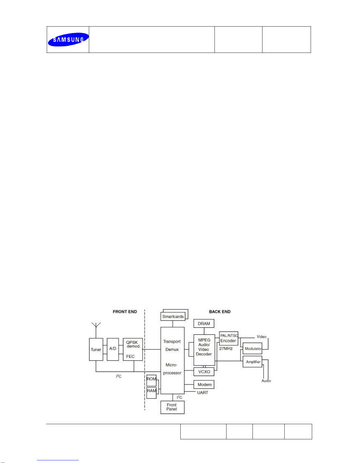
3. Overview
The DRX100 DSR(Digital Satellite Receiver) is only for BSKYB receiption which
is a CAM (Conditional Access Module) type receiver not a FTA(Free To Air) type.
The DRX100 operates with a built-in Open TV OS (OPERATING SYSTEM) software.
The signal that has been received from the satellite(ASTRA) antenna goes to the
LNB(Low Noise Blockdown Conversion) and then is transfered to I/Q signals for
QPSK demodulation. After the QPSK demodulation the signals are converted to
digital bitstreams. As the bitstreams are scrambled it goes to the DEMUX after
it has been descrambled by the CAM. The channels are identified by PIDs and
transfered to the A/V decoder.
The A/V decoder manages MPEG decoding and seperates video and analogue signals.
The video signal is encoded to analogue composite signals from the video encoder
IC(STV0119) and the audio is digital to analogue convered by varios sampling
ratio to the final TV/VCR scart outputs. The video encoder(STV0119) has a macro
vision anti-recording function to prevent recording by a VCR.
The Digibox CAS(Conditional Access System) is from NDS(News Data System) and
provides an IEE1394 port for high speed data access, a 33.6kbps modem with a
G729 voice encoder built-in, a RS232 port for serial communication and various
in/output connectors for external devices.
The CPU conbines the functionality of the STB transport IC and system
microcontroller in a single device which controls various interfaces like ;
memories, smart card access, front panel & the de/encoder interfaces.
Figure 3.1 Set Top Box architecture
SERVICE MANUAL
Document No
Date of Origin
Date of REV
51-L-DSR004
98-10-21
PAGE REV. 0 PAGE 8/102
S-00-005(96.03.27) REV.1
4. General Feature
4-1. Front & Rear Viewing
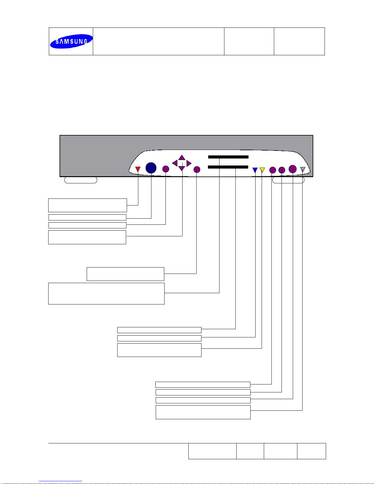
4-1-1. Front Panel
Ams trad
Red when receiving a command
from the remote control
IR Reciever Lens
Shows the previous screen
Moves the highlight around the
screens or changes channels
Chooses the highlighted option
or confirms your choice
Insert your interactive card here when using
interactive services(once available) and only
when an instruction to do so appears on-screen
Insert your sky viewing card here
Yellow when Message waiting
Green when digibox is on-line
(using the phone line)
Shows the TV Guide screen
See information about the programme
Turns the digibox on or off
Green when digibox is on
Red when digibox is off
SERVICE MANUAL
Document No
Date of Origin
Date of REV
51-L-DSR004
98-10-21
PAGE REV. 0 PAGE 9/102
S-00-005(96.03.27) REV.1
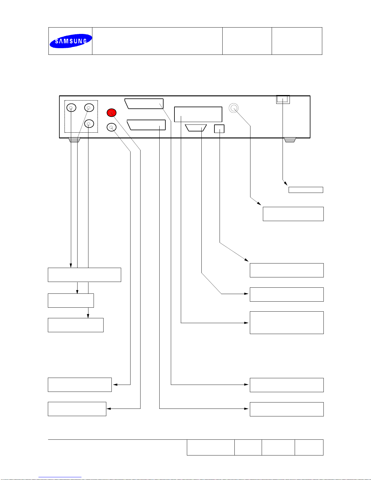
4-1-2. Rear Panel
TV SCART
VCR SCART
Left
Right
RS232
230V AC 50Hz~
13/18V DC
350mA max
Dish Input
RF Out-2 : TV RF in or
for accessory connections
RF Out-1 : TV RF
INPUT
Aerial In : For
terestrial input
Audio R : RCA jack
for audio right(red)
Audio L : RCA jack for
audio left(white)
power cord
dish input : connect
to LNB out
telephone jack : connect
to telephone line
Sreal jack : connect
to PC Serial port
digital interface :
connect to PCMCIA
interface card
VCR scart : connect to
VCR scart jack
TV scart : connect to
TV scart jack
SERVICE MANUAL
Document No
Date of Origin
Date of REV
51-L-DSR004
98-10-21
PAGE REV. 0 PAGE 10/102
S-00-005(96.03.27) REV.1
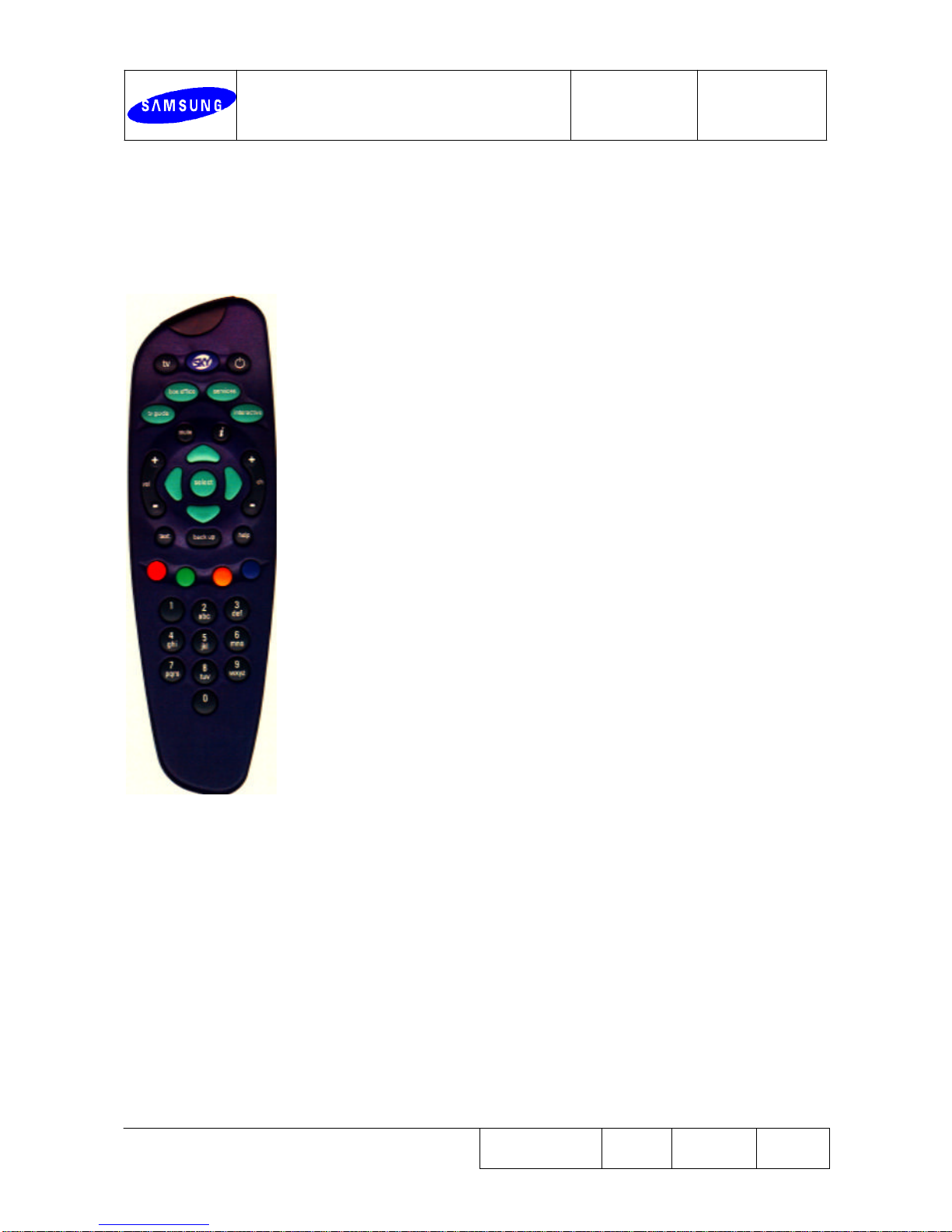
4-1-3. Remote Control Unit
4-1-3-1.
TV
: Sets your remote control to control
your TV
4-1-3-2.
SKY
: Sets your remote control to control
your Digibox
4-1-3-3.
Power
: Turns your Digibox(or TV) on and off
4-1-3-4.
box office
: Shows the Box Office screeen
4-1-3-5.
services
: Shows the Customer Service
4-1-3-6.
TV guide
: Shows the TV Guide
4-1-3-7.
interactive
: Shows the Interactive Service
4-1-3-8.
mute
: Turns the TV sound off/on
4-1-3-9.
information
: Shows information about the programme
you have highlighted
4-1-3-10.
vol
: Changes the TV volume
4-1-3-11.
select
: Chooses the option you have highlighted
or confirms your choice
4-1-3-12.
Arrow Buttons
: Moves the highlight around the screen
to highlight the option you want
4-1-3-13.
ch
: Changes the channel
4-1-3-14.
text
: Switches to text mode
4-1-3-15.
help
: For help on using the SkyGuide
4-1-3-16.
color key
: use to select the corresponding colour
option on-screeen
4-1-3-17.
backup
: Shows the previous screeen
4-1-3-18.
Numeric keys
: For selecting channel numbers or
on-screeen options
SERVICE MANUAL
Document No
Date of Origin
Date of REV
51-L-DSR004
98-10-21
PAGE REV. 0 PAGE 11/102
S-00-005(96.03.27) REV.1
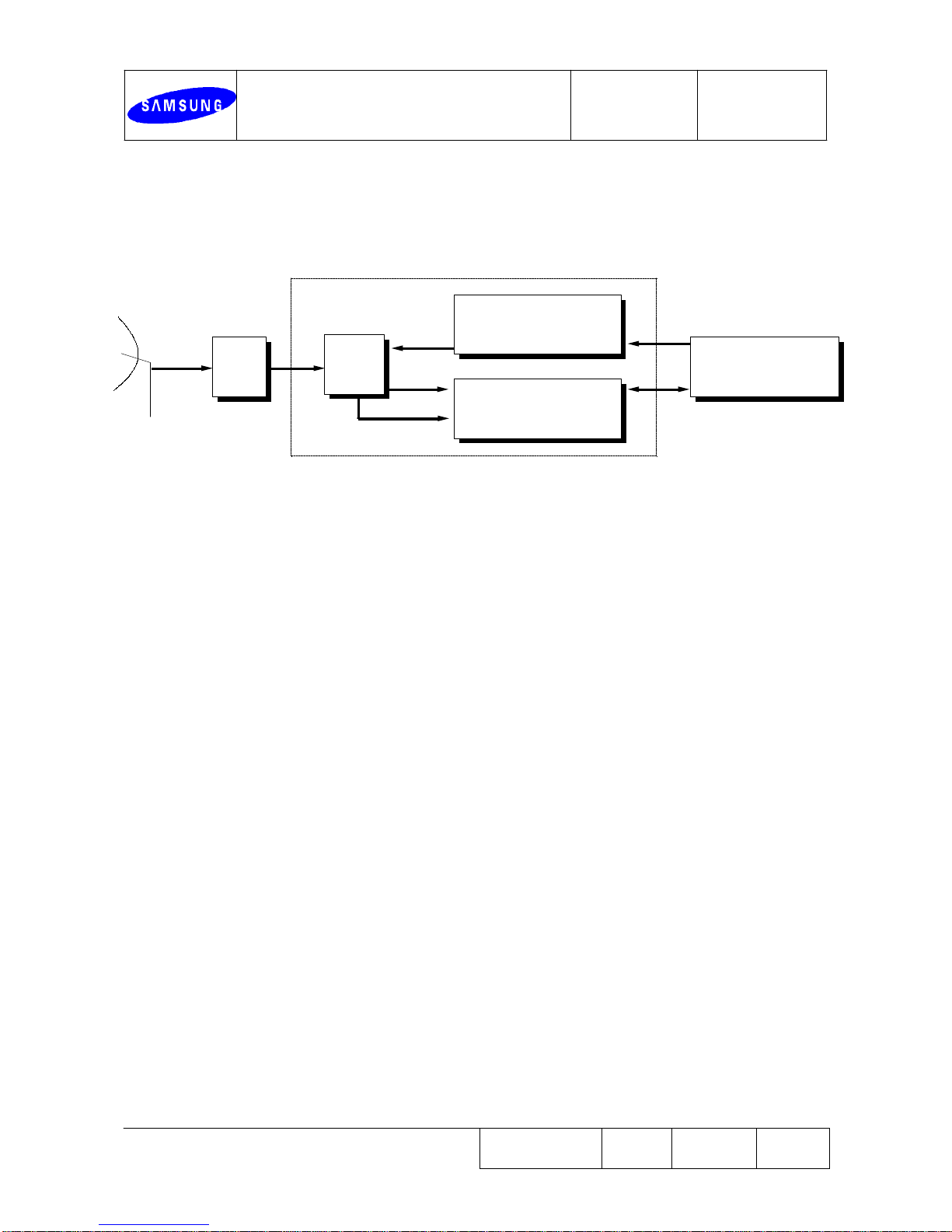
4-2. Tuner
a LNB (Low Noise Block Down Converter) converts the incoming satellite
signal from 12GHz down to an intermediate frequency (IF) of 1 GHz to 2 GHz.
Then a PLL frequency synthesizer further down converts the signal to a
second IF (479.5MHz).
The DEMUX (with microprocessor) adjusts the frequency delivered by this
circuit in such a way that the IF signal falls within the bandwidth of the
IF surface acoustic wave (SAW) filter.
The I/Q down converter translates the IF signal to baseband.
TUNER
LNB
DiSEqC 22KHz Block
QPSK Demodulator
DEMUX (ST20TP2)
I
Q
Figure 4.2 QPSK Block Diagram

SERVICE MANUAL
Document No
Date of Origin
Date of REV
51-L-DSR004
98-10-21
PAGE REV. 0 PAGE 12/102
S-00-005(96.03.27) REV.1
4-2-1. input frequency range : 950¡-2150 MHz
4-2-2. input power level : -65¡--25 dBm
4-2-3. first IF frequency : 479.5 MHz
4-2-4. maximum input level : 0 dBm
4-2-5. input connector type : IEC 169-24 (F-type)
4-2-6. input impedance : 75
¥Ø
4-2-7. input return loss : >8 dB
4-2-8. LNB current : 350 mA max
4-2-9. surge protection level : > 5kV
4-2-10. IF bandwidth : 26MHz/-1dB and 33MHz/-1dB
4-2-11. tuning increment : 125 KHz
4-2-12. signal acquisition range : +/- 10 MHz
4-2-13. AFC tracking range : +/- 2 MHz
4-2-14. channel selection : PLL frequency synthesizer
4-2-15. PLL controll interface :
I C
2
bus
4-2-16. out of band rejection :¡Ã30 dB (in band being the bandwidth
where 99% of the signal energy is)
4-2-17. AGC level adjustment step : 0.5 dB
4-2-18. AGC VOLTAGE : 0¡-5V
4-2-19. Amplitude distortion :
¡Â
0.8 dB
4-2-20. phase distortion :
¡Â5¡Æ
4-2-21. LO phase noise :
¡Â
-50 dBc/Hz (@ 1 kHz)
:
¡Â
-75 dBc/Hz (@ 10 kHz)
:
¡Â
-95 dBc/Hz (@ 100 kHz)
4-2-22. OUTPUT SIGNAL : I, Q ANALOG OUTPUTS WITH 600mV
P-P
( load 1K¥Ø,15pF at 2.5V AGC )
4-2-23. IM2 discrimination : -40dB (for two input carriers
at -25dBm)

SERVICE MANUAL
Document No
Date of Origin
Date of REV
51-L-DSR004
98-10-21
PAGE REV. 0 PAGE 13/102
S-00-005(96.03.27) REV.1
4-3. LNB Control Signal
LNB control signal is used to select frequency band (low/high band), either
conventional(22KHz tone) signalling or the new signalling method(DiSEqC)
could be used to control the switch.
The DiSEqC system is a communication bus between satellite receivers/IRDs
and satellite peripheral equipment,using only the existing coalial cable.
This single master microcontroller-based system is bi-directional and
enables controlling of satellite peripherals like;
- LNBs
- multi-switches
- SMATV switch nodes
- antenna positioners
- polarizer control units
- other devices
4-3-1. LNB control frequency : 22 kHz¡¾2 KHz
4-3-2. duty cycle : 50%¡¾10%
4-3-3. control signal amplitude : 0.6 V¡¾0.2V p-p
4-3-4. transition time : 10
§Á ¡¾5§Á
4-3-5. source impedance :¡Â50
§Ù
4-3-6. LNB supply voltage : 12.5 - 14.0 (vertical)
: 17.0 - 19.0 (horizontal)
4-3-7. DiSEqC Bus functional spec : V4.1, at level 1.1

SERVICE MANUAL
Document No
Date of Origin
Date of REV
51-L-DSR004
98-10-21
PAGE REV. 0 PAGE 14/102
S-00-005(96.03.27) REV.1
4-4. Demodulator & Channel Decoder
The outcoming I/Q signal from the tuner is tranfered to the ADC (analouge to
digital conversion) for QPSK demodulation. This digital data is then channel
decoded to remove various noise and error corrected that can occur during
satellite transmittion.
Channel decoding is accomplished by VITEBI decoding(inner FEC) and RS decoding
(outer FEC). Most RS decoders have the function for de-interleaving and remove
energy dispersal.
4-4-1. demodulation method : QPSK
4-4-2. inner FEC : VITERBI convolution
4-4-3. symbol rates : 20 ~ 30 Msym/s, step 0.1Msym/s
4-4-4. symbol rate lock range : 110 ppm
4-4-5. convolutional code rates : 1/2, 2/3, 3/4, 5/6, 7/8. K=7
(depend on BIT stream)
4-4-6. outer FEC : reed solomon decording (204,188) T=8
4-4-7. bit error rate : 1¡¿10
-11
max
4-4-8. deinterleaving : convolutional, depth I=12
4-4-9. implementation loss :¡Â0.5 dB, 0.8 dB max
at AWGN, 4.1 dB < Rs/No < 8.5 dB
4-4-10. data acquisition time :¡Â300 msec

SERVICE MANUAL
Document No
Date of Origin
Date of REV
51-L-DSR004
98-10-21
PAGE REV. 0 PAGE 15/102
S-00-005(96.03.27) REV.1
4-5. DEMUX & CPU
A Transport Demultiplexing integrates all audio, video, and data service MPEG-2
transport layer functions, the DEMUX's principle operation is straight forward:
4-5-1. A stream of data packed in transport layer format 188 bytes per packet
enters the DEMUX IC through its channel decoder interface.
The DEMUX system or IC detects the sync byte, which is the first byte of
every transport packet header. Once in sync, byte, byte-aligned data is
posted to the next stage of processing.
4-5-2. The DEMUX parses the incoming data using its Packet ID(PID) processor.
Upon user programming the DEMUX extracts the user selected program,
audio, and video Packetized Elementary Stream(PES) data, Program
Specific Information(PSI), Service Information(SI), and Private Data.
4-5-3. The selected audio and video PES layer encoded data stream is output
through the DEMUX.
4-6. A/V DECODING
Video Compression & Decompression Concepts The MPEG standards define a format
for compressed digital video.
Encoders designed to work within the confines of the standard compress video
information, and decoders decompress it. The MPEG algorithms for video
compression and decompression are flexible, but generally fit the following
criteria.
4-6-1. Data rates are about 1 to 1.5Mbit/sec for MPEG-1 and up to 15Mbit/sec
for MPEG-2. The MPEG-2 A/V Decoder used in DRX100 is capable of
supporting data rates up to 15Mbits/sec.
4-6-2. Resolution are about 352 pixels horizontal up to about 288 lines vertical
for MPEG-1 and 720 x 576 for MPEG-2(main profile). The A/V Decoder used
in DRX100 is capable of resolution up to 720 x 576 for either MPEG-1 or
MPEG-2.

SERVICE MANUAL
Document No
Date of Origin
Date of REV
51-L-DSR004
98-10-21
PAGE REV. 0 PAGE 16/102
S-00-005(96.03.27) REV.1
4-7. Video Encoding
For a video signal to be compressed, it must be sampled, digitized, and
converted to luminance and color difference signals (Y, Cr, Cb ).
The MPEG standard stipulates that the luminance component(Y) be sampled with
respect to the color difference signal ( Cr and Cb ) by the ratio of 4:1.
That is, for every four samples of Y, there is to be one sub-sample each of Cr
and Cb, because the human eye is much more sensitive to luminance components
than to color components.
Video sampling takes place in both the vertical and horizontal directions.
Once video is sampled, it is reformatted, if necessary, into a non-interlaced
signal.
An interlaced signal contains only part of the picture content( every other
horizontal line, for example) for each complete display scan.
The encoder must also choose which picture type is used. A picture correspond to
a single frame of motion video, or to a movie frame. There are three picture
types:
- Intracoded pictures (I-pictures) are coded without reference to any other
pictures.
- Predictive-coded pictures (P-pictures) are coded using motion compensated
prediction from the past I or P reference pictures.
- Bidirectionally predictive-coded pictures (B-pictures) are coded using motion
compensation from a previous and future I or P-pictures.
A typical coding scheme contains a mixture of I, P, and B-pictures. Typically,
an I-picture may occur every half a second, to give reasonably fast random
access, with two B-pictures inserted between each pair of I or B-pictures.

SERVICE MANUAL
Document No
Date of Origin
Date of REV
51-L-DSR004
98-10-21
PAGE REV. 0 PAGE 17/102
S-00-005(96.03.27) REV.1
4-8. Video Decoding
Video decoding is the reverse of video encoding and is intended to reconstruct
a moving picture sequence from a compressed, encoded bitstream.
Decoding is simple then encoding because there is no motion estimation performed
and there are far fewer options.
The data in the stream is decoded according to the syntax defined in the MPEG-2
standard. The decoder must first identify the beginning of a coded picture and
identify the type of picture, then decode each individual macroblock( a 16 x 16
region of video, corresponding to 16 horizontal pixels and 16 vertical display
lines.) within a particular picture.
Motion vectors and macroblock types (each of the picture types I, P, and B have
their own macroblock types) present in the bitstream, are used to construct a
prediction of the current macroblock based on past and future reference pictures
that the encoder has already stored.
Coefficient data is then inversed quantized and operated on by inverse DCT
(Discrete Cosine Transform) process that changes data from the frequency domain
to the time space domain. After the decoder processes all of the macroblocks the
picture reconstruction is completed.
If the picture just reconstructed is a reference picture (I-picture or B-picture
), it replaces the oldest stored reference picture and is used as the new
reference for subsequent pictures.
The pictures may need to be reordered before they are displayed, in accordance
with the display order instead of the coding order. After the pictures are
reordered, they may be displayed on an appropriate output device.
4-9. System Overview
A/V decoding is for use in digital audio and video-decoding systems based on the
MPEG-2 algorithm. It may consider as a "black box" that receives coded audio and
video data and produces a decoded audio and video data stream.

SERVICE MANUAL
Document No
Date of Origin
Date of REV
51-L-DSR004
98-10-21
PAGE REV. 0 PAGE 18/102
S-00-005(96.03.27) REV.1
4-10. A/V OUTPUT
4-10-1. Video
After the output of the video encoder (STV0119) it is buffered to
be output for the SCART and UHF modulator.
4-10-2. Audio
After the output of the OPAMP it is buffered to be output for the
SCART and RCA jack and UHF modulator.
4-10-3. scart - TV output : composite video, R, G, B, audio(L,R)
VCR output : composite video, audio(L,R)
4-10-4. phono out audio : Left audio (white), Right audio (red),
RF modulator (mono)
Video Output Impedance is 75§Ùand the connector is scart type. In Play mode,
VCR signal is routed automatically so TV viewing is possible.
4-11. RF Modulator
RF modulator is PAL I PLL type and it can select CH21 ~ CH69. Output impedance is
75§Ù, connector is EIA type, and pre set channel is CH68. When an external device
output is connected to terrestrial in port, TV viewing is possible by the signal
coming from RF out1 and 2. RF out2 serves as RCU's input signal port. Instead of
using front IR, it can be used RCU remote signal controlled by an accessory box
which means that STB's functions like channel changing and volume can be
controlled by remote control.
4-11-1. RF input
4-11-1-1. frequency range : 47 - 862 MHz
4-11-1-2. input impedance : 75
§Ù
4-11-1-3. RF bypass gain : 5 dB¡¾2 dB
4-11-1-4. isolation : >20 dB
4-11-2. RF output
4-11-2-1. frequency range : 47 - 862 MHz
4-11-2-2. output impedance : 75
§Ù
4-11-2-3. modulator output range : 471 - 862 MHz (ch21 - 69)

SERVICE MANUAL
Document No
Date of Origin
Date of REV
51-L-DSR004
98-10-21
PAGE REV. 0 PAGE 19/102
S-00-005(96.03.27) REV.1
4-11-2-4. output level : 70 dB
§Å ¡¾
5 dB
§Å
4-11-2-5. video modulation depth : 80¡¾8 %
4-11-2-6. default output channel : 68
4-11-3. Additional RF output
4-11-3-1. frequency range : 47 - 862 MHz
4-11-3-2. output Voltage : 9¡¾1 V
4-11-3-3. maximum current : 100mA
4-11-3-4. carrier frequency : 4.5 - 10 MHz
4-11-3-5. signal level "0" (p-p) : 0.5 V
4-11-3-6. signal level "1" (p-p) : 2¡¾0.15 V
4-11-3-7. input impedance : >1K§Ù(at carrier frequency)
4-12. RS232 port
STB provides 9 pin RS232 serial port for communication with PC. The monitoring
of the STB and the command delivering from PC is done via hyper terminal.
Moreover, G.729 audio data can be delivered in real time to G.729 decoder
and to STB memory via the EIA232A (RS232) port.
4-13. ICAM
ICAM contains all descrambling and CA functions supported by NDS (News Digital
Systems). ICAM uses MBM87F2011 chip to capture PID for EMM and ECM streams,
a descrambler, a smart card interface, an interface to main microcontroller,
and NDS security functions.
4-14. Smart Card Interface
The STB uses the Philips Semiconductors TDA 8004 to implement the electrical
interface to the NDS conditional access smart card slot The smart card reader
interface shall be subject to approval by NDS.
4-15. Second Smart Card (MONDEX)
The Second Smart card interface uses the Philips Semiconductors TDA 8006. Mondex
card reader is capable of reading cards entered chipside facing upwards, and
chipside facing downward The second smart card slot supports T=0 and T=1
protocols.

SERVICE MANUAL
Document No
Date of Origin
Date of REV
51-L-DSR004
98-10-21
PAGE REV. 0 PAGE 20/102
S-00-005(96.03.27) REV.1
4-16. PSTN MODEM
TCP /IP streams is delivered via the PSTN with either real-time transfer of
data identified as G.729A audio to the G.729A decoder, or to STB memory.
MODEM used in the STB supports data transmission rate of 33.6kbps.
4-17. G.729A
On line audio data is sampled at 8kHz and delivered via the MODEM, or the EIA232
port. G.729 decoder stores the transmitted data into the RAM and send it again
to L,R channel output after decoding this data.
4-18. IEEE1394
The objective of IEEE 1394 data port is to transmit and receive TS stream among
the devices and transmit DVB TS Stream received from the module to ICAM at data
rate of 25Mbps. Asynchronous input/output data rate between CPU and IEEE 1394
is 2Mbps and it is realized through the host parallel interface(1284).
Electrical and mechanical specifications of IEEE 1394 are as follows:
4-18-1. It uses a 68 pin PCMCIA/JEIDA type edge connector.
4-18-2. It provides independent Transport Stream input/output paths.
4-18-3. It supports parallel 8-bit communication and an I2C path for control of
the module.
4-18-4. All I/O signals of its connector is 3.3V logic level.
4-19. Power Supply
4-19-1. switching mode power supply
4-19-2. AC 95V ~ 240V¡¾15%
4-20. Size & Weight
- 365(W) X 265(D) X 62(H) , 1.7KG

SERVICE MANUAL
Document No
Date of Origin
Date of REV
51-L-DSR004
98-10-21
PAGE REV. 0 PAGE 21/102
S-00-005(96.03.27) REV.1
5. Technical Specification
5-1. System Specifications
5-1-1. TV system : PAL I
5-1-2. symbol rates : 20Msym/s ~ 30 Msym/s, STEP 0.1Msym/s
5-1-3. demodulation method : QPSK (DVB specification)
5-1-4. inner FEC : viterbi convolutional coding
rate 1/2, 2/3, 4/3, 5/6, 7/8. K=7 (DVB)
5-1-5. outer FEC : reed solomon decording (204,188) T=8(DVB)
5-1-6. system decoding : ISO/IEC 13818-1(MPEG2) TS specification
TS descrambling
5-1-7. video decoder : 13818-2(MPEG2) MP@ML
11172-2(MPEG1) compatible
wide screen TV (16:9) / normal TV (4:3)
5-1-8. picture resolution : 720(H)¡¿480(V)
¡¿
50 fields/sec
560(H)
¡¿
480(V)
¡¿
50 fields/sec
480(H)
¡¿
480(V)
¡¿
50 fields/sec
360(H)
¡¿
480(V)
¡¿
50 fields/sec
5-1-9. audio decoder : ISO/IEC 11172-3(MPEG1) layer 1, 2
multi-lingual
sampling frequency - 32, 44.1, 48 KHz
operation mode - stereo, dual, mono,
joint stereo

SERVICE MANUAL
Document No
Date of Origin
Date of REV
51-L-DSR004
98-10-21
PAGE REV. 0 PAGE 22/102
S-00-005(96.03.27) REV.1
5-2. System Features
5-2-1. dimensions : 365(w) x 265(d) x 62(h)
5-2-2. operating temperature : 0¡É~ 40
¡É
5-2-3. storage temperature : -20¡É~ 60
¡É
5-2-4. humidity : operating --- up to 95%
storage --- less than 90%
5-2-5. remote control : full function infra-red remocon (35 keys)
5-2-6. front panel control : power,¡ã/¡å,¢¸/¢º, back up, select, TV
guide, i (information)
5-3. Power Supply
5-3-1. power supply type : SMPS
5-3-2. input voltage : 95V - 240 Vac / 50 Hz
5-3-3. protection : internally fused
5-3-4. output voltage : 18V
GND
28V
8V
12V
GND
3.3V¡¾0.25V
5V
¡¾
0.25V
GND
5-3-5. LNB power supply : 13V/18V ,350mA max (switchable)
5-4. Composite Video Output
5-4-1. composite video : PAL I
5-4-2. output level : 1V p-p (load 75¥Ø)
5-4-3. impedance : 75
¥Ø
5-4-4. connector : scart (TV/VCR)
5-4-5. S/N ratio : 60 dB (luminance weighted)

SERVICE MANUAL
Document No
Date of Origin
Date of REV
51-L-DSR004
98-10-21
PAGE REV. 0 PAGE 23/102
S-00-005(96.03.27) REV.1
5-5. Audio Output
5-5-1. operating mode : stereo, dual, mono, joint stereo
5-5-2. output level : 2.0¡¾0.2V p-p
5-5-3. output connector : RCA phone jack (female)
5-5-4. Left / Right balance :¡¾2 dB max
5-5-5. S/N ratio : 80 dB min
5-6. RF Modulator Output
5-6-1. TV standard : PAL I
5-6-2. output level : 70 dB
§Å ¡¾
5 dB
§Å
5-6-3. modulator output range : 471 - 862 MHz (ch21 - 69)
5-6-4. default output channel : CH68
5-6-5. connector : EIA type (female)
5-6-6. output audio : mono
5-7. R.G.B Output
5-7-1. output level : 0.7Vp-p¡¾0.1V (load 75¥Ø)
5-7-2. impedance : 75
¥Ø
5-8. Asynchronous Data Output
5-8-1. standard : RS232
5-8-2. bit rate : 115200 bps
5-8-3. connector type : 9 pin D-type

SERVICE MANUAL
Document No
Date of Origin
Date of REV
51-L-DSR004
98-10-21
PAGE REV. 0 PAGE 24/102
S-00-005(96.03.27) REV.1
6. Diagnostics
6-1. Preparations
6-1-1. Personal Computer (With 486 CPU or higher)
6-1-2. RS232 Cable for communication
6-1-3. OS (Windows 3.1 or higher)
6-2. Setup
6-2-1. Connect the 9 pin connector(RS232 Null Modem cable) of IRD (on the
back panel) to the serial port of the PC or terminal (115200,N,8,1)
6-2-2. Turn on the PC
6-2-3. Select Winfile manager to execute BskybTerm.
6-2-4. Configurate the Port and Baudrate as below;
Port : Select to COM port currently used.
Baudrate : 115200
6-2-5. Turn on the STB.
For normal operation the following messages will display on the PC screen,
.
.
.
set LNB freq (lo 9750000, hi 10600000, sw 11700000)
tv status 2!
Set TV to CBVS
Send Ok
#CONTROL[running] unknown control error=0x10
new scan parameters
fixed parameters invalid - IGNORED
new scan request
scan: freq 11778000, sr 27500000, pol 1 (0=H, 1=V), direction 0
tune 1178000KHz, 27500Ksps Auto
scan lock
Welcome to Test tool V1.00
Tool>
Press 'ESC' here

SERVICE MANUAL
Document No
Date of Origin
Date of REV
51-L-DSR004
98-10-21
PAGE REV. 0 PAGE 25/102
S-00-005(96.03.27) REV.1
6-3. Function keys
T1 or F1 : Is to turn 22KHz on, 18V on and set the LNB to Horizontal and
Set to TV mode RGB & 16:9, RF ON, MOD +9V ON, MOD Led 0 to 3 BLINK,
infinite BEEP on, GVOL 00 and FF, Audio H/W muted.
T2 or F2 : Is to turn 22KHz off, 14V off and set the LNB to Vertical and
Set to TV mode CBVS & 4:3, infinite BEEP off, MOD +9V OFF.
T3 or F3 : is to check IEEE1394 data port (addr : 0, wr data : 0, rd data : 0
to addr : 17, wr data : 17, rd data : 17, CD2:1, MOD_I2C:1, INT:1)
T4 or F4 : Is to turn on Front LED 0 to 3 BLINK
T5 or F5 : is to check G.729 stream (ex : g729 playing, G729A mode, G729
Decoder is enabled, G729 audio stop)
T6 or F6 : is to check CA system (ex : Card is not inserted, removed...)
T7 or F7 : is to check video Contrast (ex : Set TV to CBVS, CVBS :-10, CVBS :
+10, Set TV to RGB, RGB :-10, RGB :+10)
T8 or F8 : is to check and write FLASH rom
T9 or F9 : is to check Modem port (ex : DTMF, PULSE)
F10 to F12 is for additional future features to analyze the set top box.

SERVICE MANUAL
Document No
Date of Origin
Date of REV
51-L-DSR004
98-10-21
PAGE REV. 0 PAGE 26/102
S-00-005(96.03.27) REV.1
7. Trouble Shooting
7-1.
Instrument
7-1-1. Transmmiter
7-1-1-1. TEKTRONIX MODULATOR (DVT200)
7-1-1-2. TSG or MTG200 (MPEG test generator)
7-1-1-3. QPSK modulator
7-1-1-4. DATA CD for EPG (distributed from BSKYB)
or
7-1-1-5. dish input signal
7-1-2. Checker
7-1-2-1. VM700A (audio/video signal analyzer)
7-1-2-2. analog or digital oscilloscope
7-1-2-3. spectrum analyzer
7-1-2-4. PC (i486 & windows 3.1 system or higher)
7-1-2-5. multimeter
7-1-3. Accessory
7-1-3-1. TV (PAL type)
7-1-3-2. RS232C 9pin cable
7-1-3-3. scart cable
7-1-3-4. RCA jack
7-1-3-5. iron & solder...
SERVICE MANUAL
Document No
Date of Origin
Date of REV
51-L-DSR004
98-10-21
PAGE REV. 0 PAGE 27/102
S-00-005(96.03.27) REV.1
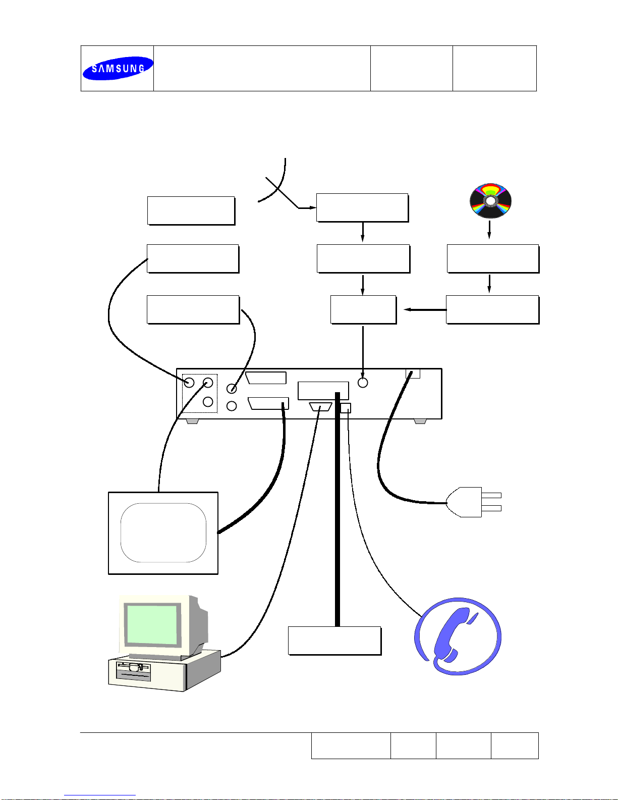
7-2. Installation
TV SCART
VCR SCART
Left
Right
RS232
230V AC
50Hz~
13/18V DC
350mA max
Dish Input
Multimeter
Spectrum
Oscilloscope combiner
TV
LNB
DiSEqC module
TSG
DVT200
2'nd DIGI BOX

SERVICE MANUAL
Document No
Date of Origin
Date of REV
51-L-DSR004
98-10-21
PAGE REV. 0 PAGE 28/102
S-00-005(96.03.27) REV.1
plug in Power Cord
FUSE OK?
Replace FUSE &
Check SMPS
Replace SMPS
S/W Initalize
Replace Main PCB
Enter Function Key
Function OK?
Check SMPS
Output Pins
No
Yes
another Check?
Yes
No
Yes
Yes
Signal pass OK?
No
No
Modify OK?
Modify Circuit
Yes
No
AC Input?
No
Yes
No
Check Circuit
END
Yes
No
7-3. Basic Flow Chart

SERVICE MANUAL
Document No
Date of Origin
Date of REV
51-L-DSR004
98-10-21
PAGE REV. 0 PAGE 29/102
S-00-005(96.03.27) REV.1
7-4. SMPS
7-4-1.
The SMPS's Fundamental Operation
The present circuit uses the commercial power supply of AC230V. The power is
supplied at the F1 Live part and Neutral part when the AC power is On. During
this operation, the TH1 THERMISTOR protects the semiconductor devices from a
sudden current and the TNR1 Varistor protects the semiconductor devices setted
behind the Fuse of the AC Suge Voltage (> AC 380V).
Capacitors C1,C2, and inductor L1 are Filter circuit which eliminate the noise
introduced from a AC Line and the noise, originated from an internal circuit,
flowing to AC Line.
The voltage, passed through the Filter circuit, is rectified by DC Diode (D1 D4) and after this wave is smoothed by a capacitor C3 and finally it is supplied
to Q1's DRAIN through the Primary Trans.
The rectified voltage is changed to around DC 310V calculated by the equation
V=¡î2 V and it is called Vin. Also, when the Vcc power is supplied to Q1 SMART IC
through R2, Q1 SMART IC internal circuit works and supplies GATE Signal of 50KHz
to the GATE of Q1 SMART IC.
The Dnn voltage of Q1 is by passed to Ground when Q1 SMART IC is turned on.
In this process, the FEEDBACK PIN of SMART IC serves as a function to regulate
voltage level and to protect from an excessive load simultaneously.
The method used for the voltage regulation is Current Mode Control method which
modulate the width of PWM DUTY comparing the error voltage detected by PHOTO
COUPLER and the value of MOSFET DRAIN Current detected by current detection
resistor. In the process, it also occurs an inverse power at Secondary trans.
This kind of circuit is PWM type and this cycle is realized continuously.
The working frequency is fixed at 50kHz. The working switching pulse is taken to
the Secondary trans where it absorves the energy by resonating the frequency
oscillation with L and C of Secondary Trans (F=1/2
¥ð ¡î
L C).
This energy is rectified by Diode and it is smoothed by a capacitor and finally
 Loading...