

Samsung D61B Training Manual

CONTENTS
Precautions
Reference Information
Specifications
Introduction PDP
Alignment and Adjustments
Troubleshooting
Circuit Description
Handling Description
Glossary
Schematic Diagrams
1.
2.
3.
4.
5.
6.
7.
8.
9.
10.
PLASMA DISPLAY TV
PLASMA DISPLAY TV
Chassis : D61B

ELECTRONICS
© Samsung Electronics Co., Ltd. Mar. 2004
Printed in Korea
AA82-01375A
This Service Manual is a property of Samsung Electronics Co.,Ltd.
Any unauthorized use of Manual can be punished under applicable
International and/or domestic law.
1. Precautions
1-1 Safety Precautions
1. Be sure that all of the built-in protective
devices are replaced. Restore any missing
protective shields.
2. When reinstalling the chassis and its
assemblies, be sure to restore all protective
devices, including: nonmetallic control knobs
and compartment covers.
3. Make sure that there are no cabinet openings
through which people—particularly
children—might insert fingers and contact
dangerous voltages. Such openings include
the spacing between fornt cabinet and back
cabinet, excessively wide cabinet
ventilation slots, and improperly fitted back
covers.
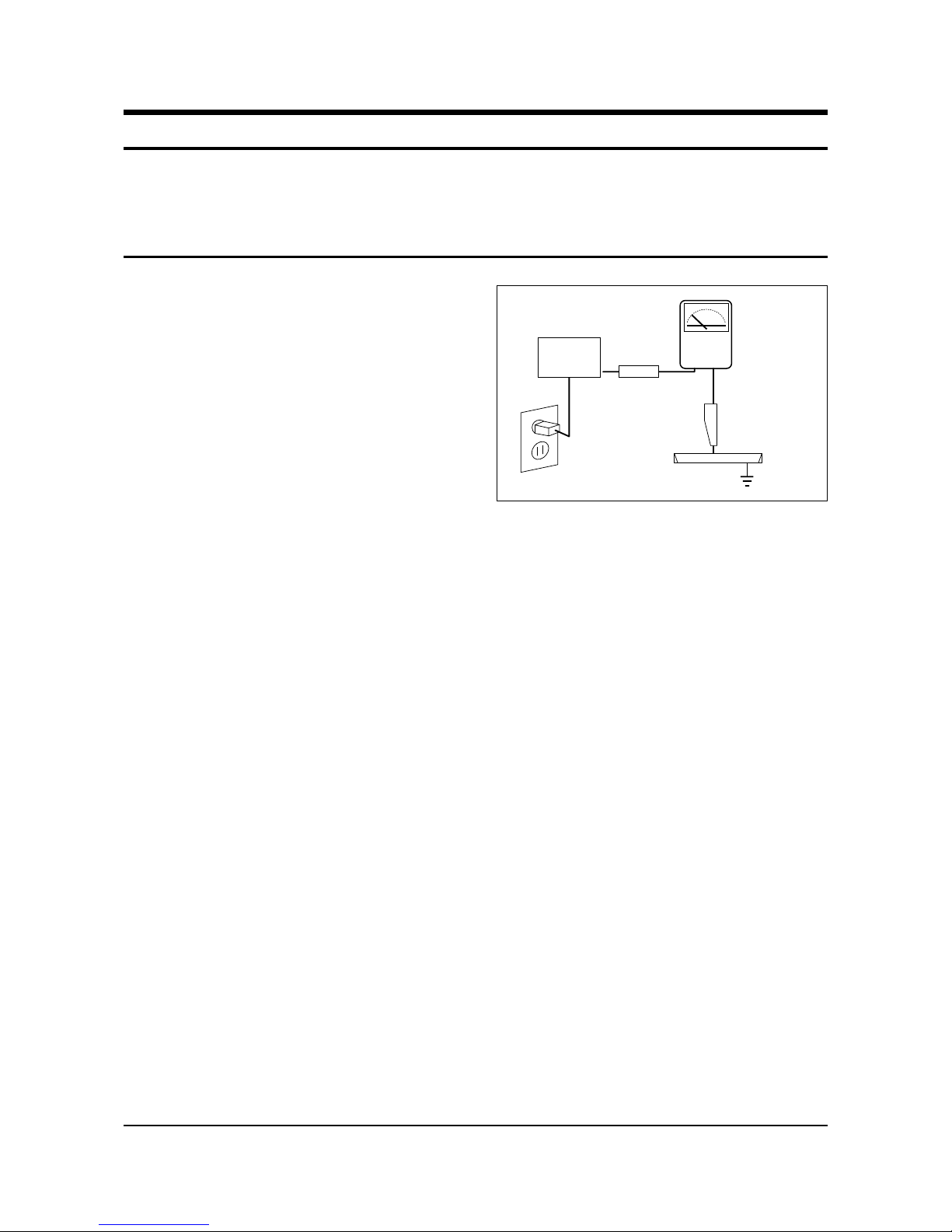
4. Leakage Current Hot Check (Figure 1-1):
Warning: Do not use an isolation
transformer during this test. Use a leakagecurrent tester or a metering system that
complies with American National Standards
Institute (ANSI C101.1, Leakage Current for
Appliances), and Underwriters Laboratories
(UL Publication UL1950.5.2).
5. With the unit completely reassembled, plug
the AC line cord directly into the power
outlet. With the unit’s AC switch first in the
ON position and then OFF, measure the
current between a known earth ground (metal
water pipe, conduit, etc.) and all exposed
metal parts, including: antennas, handle
brackets, metal cabinets, screwheads and
control shafts. The current measured should
not exceed 3.5 milliamp. Reverse the powerplug prongs in the AC outlet and repeat the
test.
Fig. 1-1 AC Leakage Test
6. Antenna Cold Check:
With the unit’s AC plug disconnected from the
AC source, connect an electrical jumper across
the two AC prongs. Connect one lead of the
ohmmeter to an AC prong. Connect the other
lead to the coaxial connector.
7. High Voltage Limits:
High voltage must be measured each time servicing is done on the B+, horizontal deflection
or high voltage circuits.
Precautions
Samsung Electronics 1-1
LEAKAGE
CURRENT
TESTER
DEVICE
UNDER
TEST
TEST ALL
EXPOSED METAL
SURFACES
2-WIRE CORD
ALSO TEST WITH
PLUG REVERSED
(USING AC ADAPTER
PLUG AS REQUIRED)
EARTH
GROUND
(READING SHOULD
NOT BE ABOVE
0.5mA)
Follow these safety, servicing and ESD precautions to prevent damage and protect against potential
hazards such as electrical shock and X-rays.

1-2 Safety Precautions (Continued)
8. High voltage is maintained within specified
limits by close-tolerance, safety-related
components and adjustments. If the high
voltage exceeds the specified limits, check
each of the special components.
9. Design Alteration Warning:
Never alter or add to the mechanical or
electrical design of this unit. Example: Do not
add auxiliary audio or video connectors. Such
alterations might create a safety hazard. Also,
any design changes or additions will void the
manufacturer’s warranty.
10. Hot Chassis Warning:
Some TV receiver chassis are electrically
connected directly to one conductor of the AC
power cord. If an isolation transformer is not
used, these units may be safely serviced only
if the AC power plug is inserted so that the
chassis is connected to the ground side of the
AC source.
To confirm that the AC power plug is inserted
correctly, do the following: Using an AC
voltmeter, measure the voltage between the
chassis and a known earth ground. If the
reading is greater than 1.0V, remove the AC
power plug, reverse its polarity and reinsert.
Re-measure the voltage between the chassis
and ground.
11. Some TV chassis are designed to operate with
85 volts AC between chassis and ground,
regardless of the AC plug polarity. These units
can be safely serviced only if an isolation
transformer inserted between the receiver and
the power source.
12. Some TV chassis have a secondary ground
system in addition to the main chassis ground.
This secondary ground system is not
isolated from the AC power line. The two
ground systems are electrically separated by
insulating material that must not be defeated
or altered.
13. Components, parts and wiring that appear to
have overheated or that are otherwise
damaged should be replaced with parts that
meet the original specifications. Always
determine the cause of damage or overheating, and correct any potential hazards.
14. Observe the original lead dress, especially
near the following areas: Antenna wiring,
sharp edges, and especially the AC and high
voltage power supplies. Always inspect for
pinched, out-of-place, or frayed wiring. Do
not change the spacing between components
and the printed circuit board. Check the AC
power cord for damage. Make sure that leads
and components do not touch thermally hot
parts.
15. Product Safety Notice:
Some electrical and mechanical parts have
special safety-related characteristics which
might not be obvious from visual inspection.
These safety features and the protection they
give might be lost if the replacement component differs from the original—even if the
replacement is rated for higher voltage,
wattage, etc.
Components that are critical for safety are
indicated in the circuit diagram by shading,
( ) or ( ).
Use replacement components that have the
same ratings, especially for flame resistance
and dielectric strength specifications.
A replacement part that does not have the
same safety characteristics as the original
might create shock, fire or other hazards.
Precautions
1-2 Samsung Electronics

1-3 Servicing Precautions
1. Servicing precautions are printed on the
cabinet. Follow them.
2. Always unplug the unit’s AC power cord from
the AC power source before attempting to: (a)
Remove or reinstall any component or
assembly, (b) Disconnect an electrical plug or
connector, (c) Connect a test component in
parallel with an electrolytic capacitor.
3. Some components are raised above the printed
circuit board for safety. An insulation tube or
tape is sometimes used. The internal wiring is
sometimes clamped to prevent contact with
thermally hot components. Reinstall all such
elements to their original position.
4. After servicing, always check that the screws,
components and wiring have been correctly
reinstalled. Make sure that the portion around
the serviced part has not been damaged.
5. Check the insulation between the blades of the
AC plug and accessible conductive parts
(examples: metal panels, input terminals and
earphone jacks).
6. Never defeat any of the B+ voltage interlocks.
Do not apply AC power to the unit (or any of
its assemblies) unless all solid-state heat sinks
are correctly installed.
7. Always connect a test instrument’s ground
lead to the instrument chassis ground before
connecting the positive lead; always remove
the instrument’s ground lead last.
8. Plasma display panels have partial afterimages when a same picture continues to be displayed for a certain time. This happens due to
the degradation of brightness caused by a
scale-down effect.
To prevent such afterimages when displaying
a same picture for a certain time, be sure to
reduce the level of brightness and contrast.
ex) Contrast : 50 or 75, Brightness : 25
9. Plasma display is an array of pixels(cells).
Therefore, if at least 99.9% pixels keep normal,
the appropriate panel is judged as ‘approved
product.’ Even though some of pixels keep
luminescent or always light off, do not worry
because the panel is approved.
Precautions
Samsung Electronics 1-3
Warning 1 : First read the “Safety Precautions” section of this manual. If some unforeseen circumstance creates a
conflict between the servicing and safety precautions, always follow the safety precautions.
Warning 2 : An electrolytic capacitor installed with the wrong polarity might explode.

1-4 Precautions for Electrostatically Sensitive Devices (ESDs)
1. Some semiconductor (“solid state”) devices
are easily damaged by static electricity. Such
components are called Electrostatically
Sensitive Devices (ESDs); examples include
integrated circuits and some field-effect
transistors. The following techniques will
reduce the occurrence of component damage
caused by static electricity.
2. Immediately before handling any semicon
ductor components or assemblies, drain the
electrostatic charge from your body by
touching a known earth ground. Alternatively,
wear a discharging wrist-strap device. (Be
sure to remove it prior to applying power—
this is an electric shock precaution.)
3. After removing an ESD-equipped assembly,
place it on a conductive surface such as
aluminum foil to prevent accumulation of
electrostatic charge.
4. Do not use freon-propelled chemicals. These
can generate electrical charges that damage
ESDs.
5. Use only a grounded-tip soldering iron when
soldering or unsoldering ESDs.
6. Use only an anti-static solder removal device.
Many solder removal devices are not rated as
“anti-static”; these can accumulate sufficient
electrical charge to damage ESDs.
7. Do not remove a replacement ESD from its
protective package until you are ready to
install it. Most replacement ESDs are
packaged with leads that are electrically
shorted together by conductive foam,
aluminum foil or other conductive materials.
8. Immediately before removing the protective
material from the leads of a replacement ESD,
touch the protective material to the chassis or
circuit assembly into which the device will be
installed.
9. Minimize body motions when handling
unpackaged replacement ESDs. Motions such
as brushing clothes together, or lifting a foot
from a carpeted floor can generate enough
static electricity to damage an ESD.
Precautions
1-4 Samsung Electronics
CAUTION
These servicing instructions are for use by
qualified service personnel only.
To reduce the risk of electric shock do not
perform any servicing other than that contained
in the operating instructions unless you are
qualified to do so.

Reference Information
Samsung Electronics 2-1
2. Reference Information
2-1 Tables of Abbreviations and Acronyms
A
Ah
Å
dB
dBm
°C
°F
°K
F
G
GHz
g
H
Hz
h
ips
kWh
kg
kHz
kΩ
km
km/h
kV
kVA
kW
I
MHz
Ampere
Ampere-hour
Angstrom
Decibel
Decibel Referenced to One
Milliwatt
Degree Celsius
Degree Fahrenheit
degree Kelvin
Farad
Gauss
Gigahertz
Gram
Henry
Hertz
Hour
Inches Per Second
Kilowatt-hour
Kilogram
Kilohertz
Kilohm
Kilometer
Kilometer Per Hour
Kilovolt
Kilovolt-ampere
Kilowatt
Liter
Megahertz
MV
MW
MΩ
m
µA
µF
µH
µm
µs
µW
mA
mg
mH
mI
mm
ms
mV
nF
Ω
pF
Ib
rpm
rps
s
V
VA
W
Wh
Megavolt
Megawatt
Megohm
Meter
Microampere
Microfarad
Microhenry
Micrometer
Microsecond
Microwatt
Milliampere
Milligram
Millihenry
Milliliter
Millimeter
Millisecond
Millivolt
Nanofarad
Ohm
Picofarad
Pound
Revolutions Per Minute
Revolutions Per Second
Second (Time)
Volt
Volt-ampere
Watt
Watt-hour
Table 2-1 Abbreviations

Reference Information
2-2 Samsung Electronics
Table 2-2 Table of Acronyms
ABL
AC
ACC
AF
AFC
AFT
AGC
AM
ANSI
APC
APC
A/V
AVC
BAL
BPF
B-Y
CATV
CB
CCD
CCTV
Ch
CRT
CW
DC
DVM
EIA
ESD
ESD
FBP
FBT
FF
FM
FS
GND
G-Y
H
HF
HI-FI
IC
IC
IF
Automatic Brightness Limiter
Alternating Current
Automatic Chroma Control
Audio Frequency
Automatic Frequency Control
Automatic Fine Tuning
Automatic Gain Control
Amplitude Modulation
American National Standards Institute
Automatic Phase Control
Automatic Picture Control
Audio-Video
Automatic Volume Control
Balance
Bandpass Filter
Blue-Y
Community Antenna Television (Cable TV)
Citizens Band
Charge Coupled Device
Closed Circuit Television
Channel
Cathode Ray Tube
Continuous Wave
Direct Current
Digital Volt Meter
Electronics Industries Association
Electrostatic Discharge
Electrostatically Sensitive Device
Feedback Pulse
Flyback Transformer
Flip-Flop
Frequency Modulation
Fail Safe
Ground
Green-Y
High
High-Frequency
High Fidelity
Inductance-Capacitance
Integrated Circuit
Intermediate Frequency
I/O
L
L
LED
LF
MOSFET
MTS
NAB
NEC
NTSC
OSD
PCB
PLL
PWM
QIF
R
RC
RF
R-Y
SAP
SAW
SIF
SMPS
S/N
SW
TP
TTL
TV
UHF
UL
UV
VCD
VCO
VCXO
VHF
VIF
VR
VTR
VTVM
TR
Input/output
Left
Low
Light Emitting Diode
Low Frequency
Metal-Oxide-Semiconductor-Field-Effect-Tr
Multi-channel Television Sound
National Association of Broadcasters
National Electric Code
National Television Systems Committee
On Screen Display
Printed Circuit Board
Phase-Locked Loop
Pulse Width Modulation
Quadrature Intermediate Frequency
Right
Resistor & Capacitor
Radio Frequency
Red-Y
Second Audio Program
Surface Acoustic Wave(Filter)
Sound Intermediate Frequency
Switching Mode Power Supply
Signal/Noise
Switch
Test Point
Transistor Transistor Logic
Television
Ultra High Frequency
Underwriters Laboratories
Ultraviolet
Variable-Capacitance Diode
Voltage Controlled Oscillator
Voltage Controlled Crystal Oscillator
Very High Frequency
Video Intermediate Frequency
Variable Resistor
Video Tape Recorder
Vacuum Tube Voltmeter
Transistor

Specifications
Samsung Electronics 3-1
3. Specifications
MODEL
Display
Display
Screen Size
Voltage
Power Consumption
Number of Pixels
External Control
AUDIO Input
AUDIO Output
VIDEO Input
VIDEO Output
Dimensions
Weight
PPM42S3Q
1027(W) x 79(D) x 630.5(H) mm / 40.43(W) x 3.11(D) x 24.82(H) inches
31 Kg / 68.34 lbs (without stand)
107 Cm / 42 Inches
AC 120V, 60Hz / AC100-250V, 50/60Hz
330 Watts
852(H) X 480(V)
RS-232C IN(Mini jack), RS-232C OUT(D-SUB 9P)
VIDEO / S-VIDEO
COMPONENT 1
COMPONENT 2
RGB(PC) 1/2
DVI
External Speaker (10W+10W)
Audio Output (L/R RCA)
VIDEO
S-VIDEO
COMPONENT 1 - 480i / 480p / 720p / 1080i
COMPONENT 2/RGB2(PC) IN (BNC, 5P, 480i~1080i, VGA~XGA)
RGB1(PC1) - D-SUB 15P
DVI
Monitor Output (RCA)

3-2 Samsung Electronics
MEMO
4. Introduction PDP
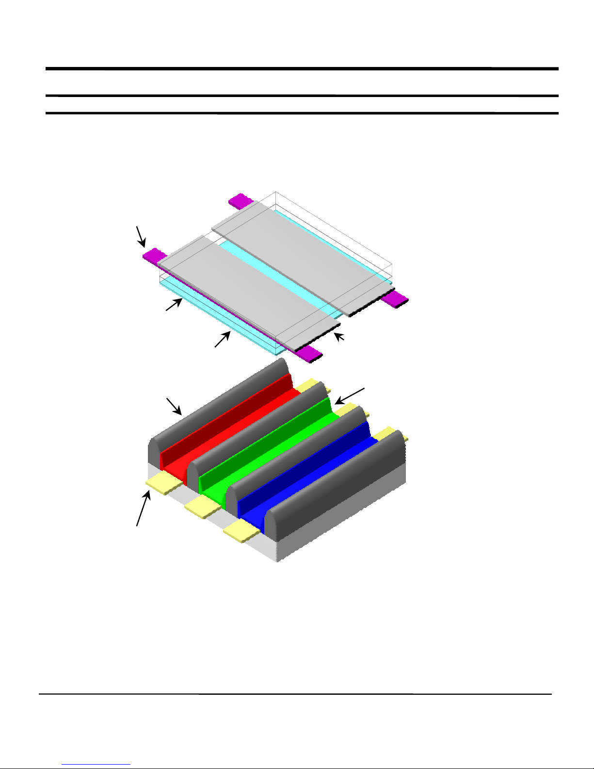
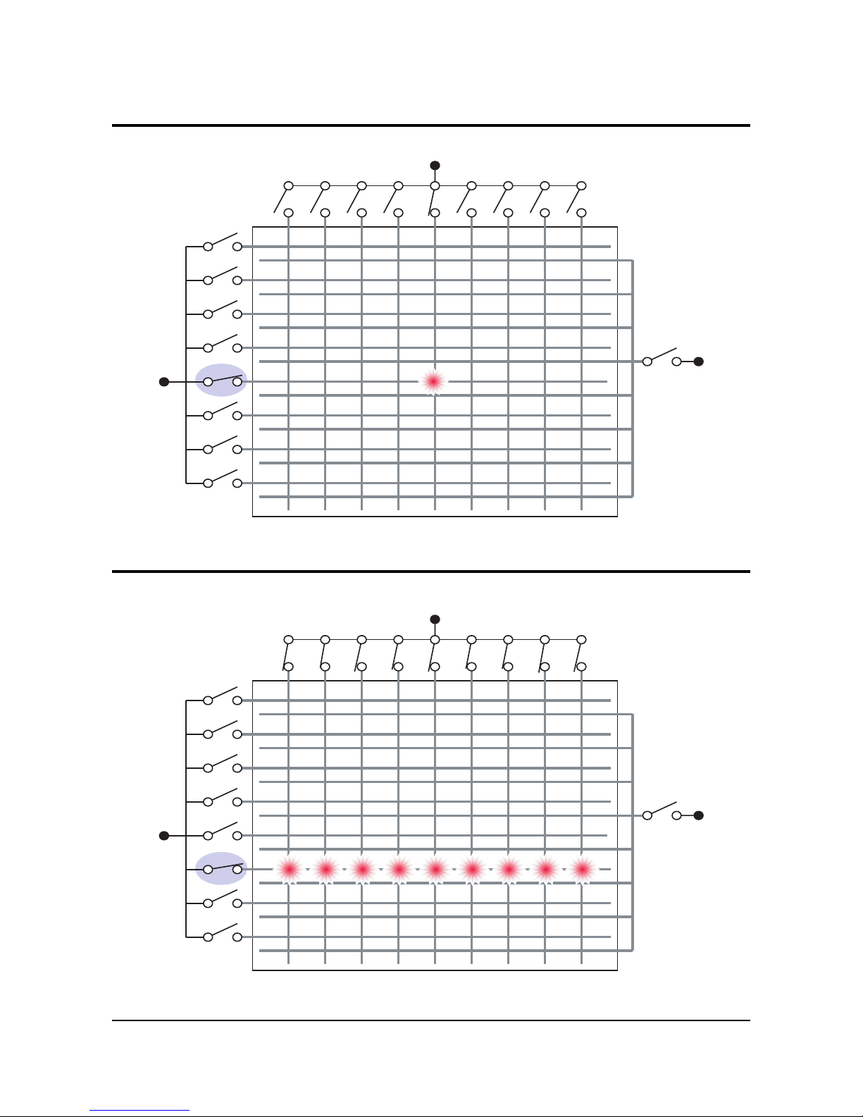
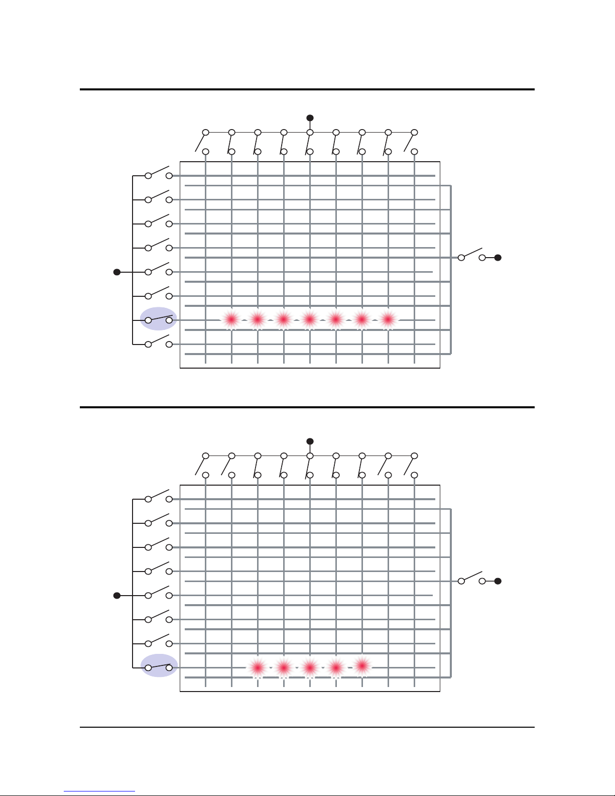
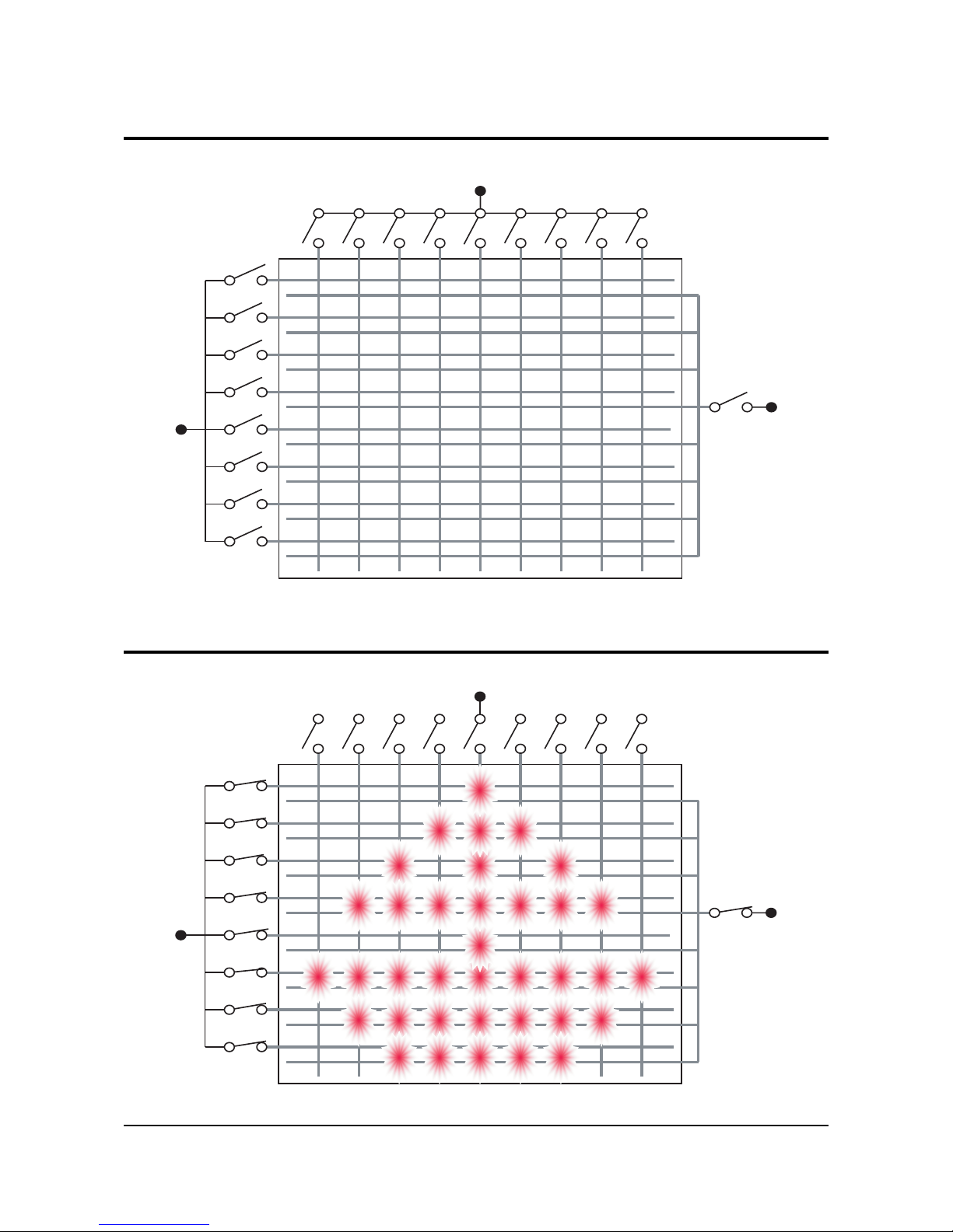
4-1 Cell Structure of PDP
Introduction PDP
Bus electrode
Dielectric
Barrier
Front panel
ITO electrodeMgO layer
Phosphors
Address
Electrode
Samsung Electronics 4-1
Back panel
Y1
Y2
Y480
X
X
X
~
~
∫
A1
A2 A3 A4 A5
A6 A7
R
e
f
e
r
e
n
c
e
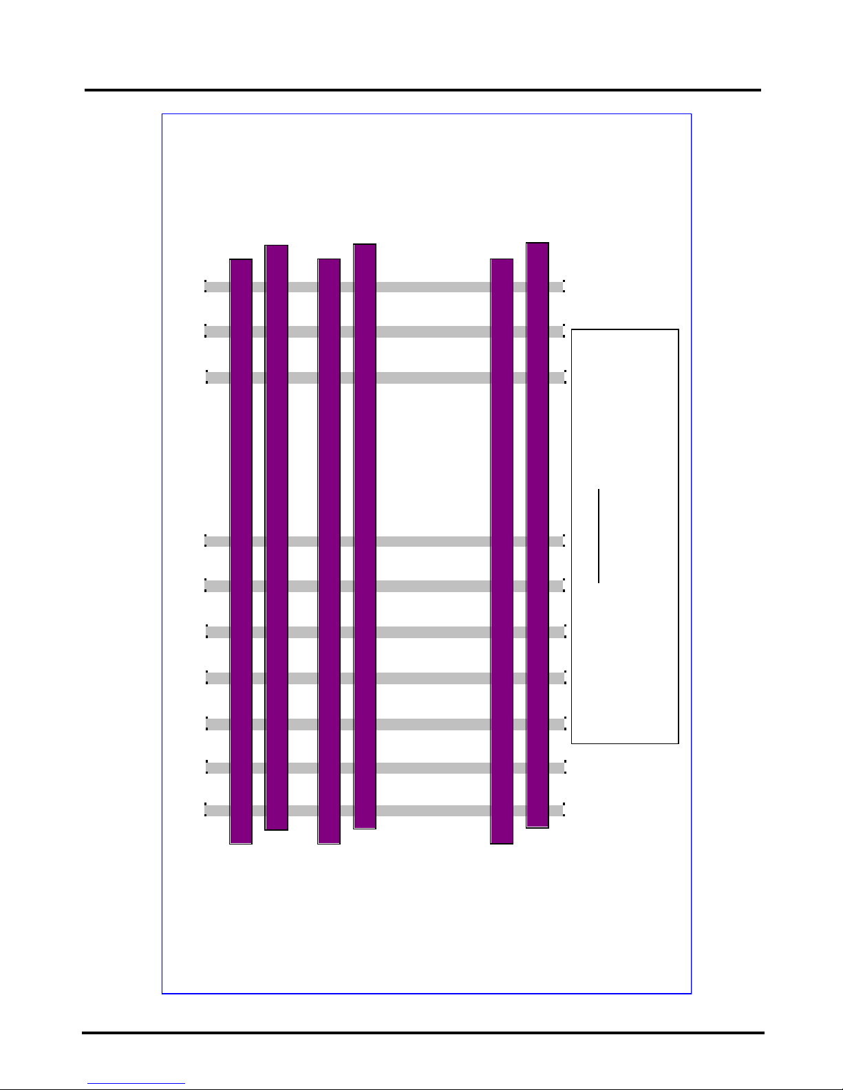
- A1,A2,,,:AddressElectrode
- Y1,Y2,,,:Scan&SustainElectrode
- X : Common & Sustain Electrode
4-2 Electrode arrangement of SD PDP
4-2
Samsung Electronics
Introduction PDP
•
•
Electrode covered with dielectric
Electrode covered with dielectric
•
•
dielectric limits current
dielectric limits current
•
•
emission from both side
emission from both side
AC
AC
-
-
PDP
PDP
V
I
V
I
Vf
X Y
Y – X
Making of Voltage
(Over Vf)
Y – X
Making of Voltage
(Over Vf)
Discharge
(Discharge Current)
Discharge
(Discharge Current)
X Y
-
+
-
+
-
+
X Y
- - - + + +
Wall Charge
(Stop Discharge)
Wall Charge
(Stop Discharge)
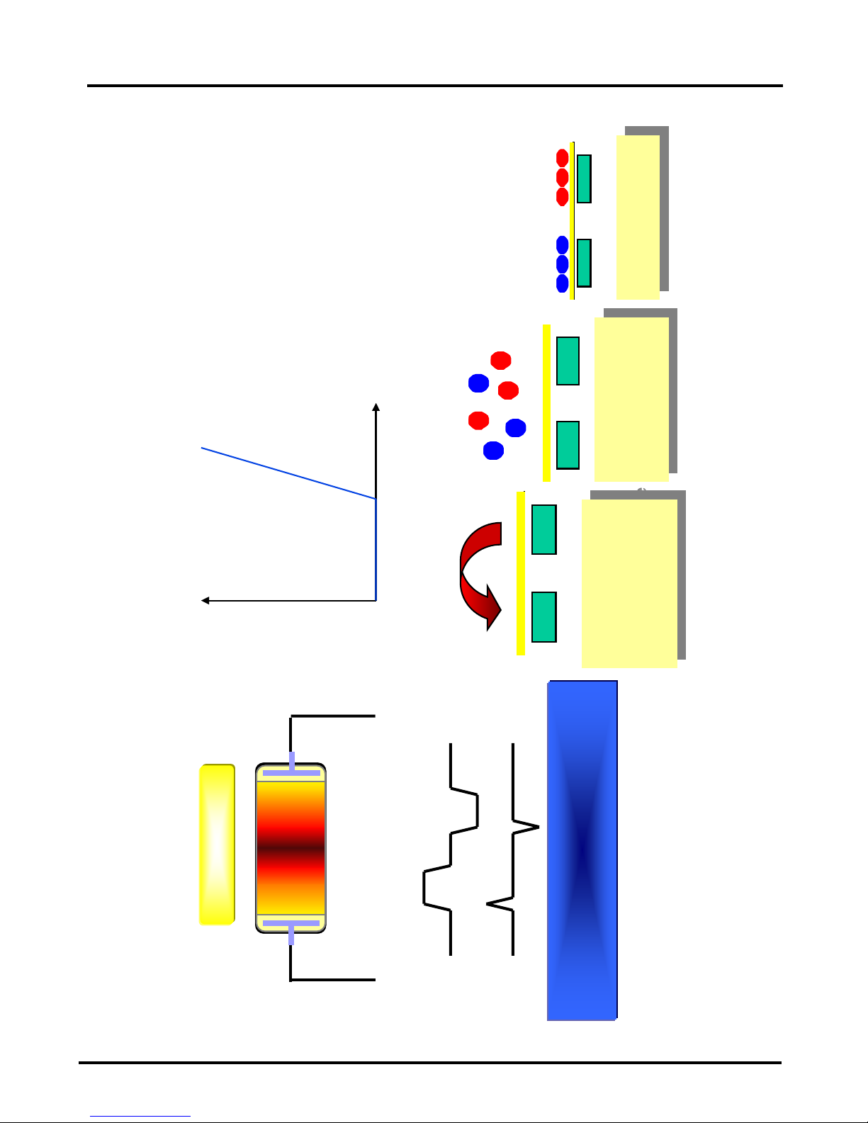
4-3 Discharge in AC PDP
Samsung Electronics
4-3
Introduction PDP
-
Seed electron
E-Field
Seed Electron : After seed electron generated in
discharge space,it is accelerated by Electric field
Seed Electron : After seed electron generated in
discharge space,it is accelerated by Electric field
-
-
+
Electron and Ion are generated by collision
Between accelerated Electron and neutrality particle.
Electron and Ion are generated by collision
Between accelerated Electron and neutrality particle.
+
-
-
+
-
-
+
Many Electrons and Ions are generated continuously
by collision.
It is end of first Discharge.
Many Electrons and Ions are generated continuously
by collision.
It is end of first Discharge.
4-4 Discharge Mechanism - Process
4-4 Samsung Electronics
Introduction PDP
secondary electron
E-Field
-
-
+
When Ion conflict with Cathode, it is generate
2
nd
Electron.
(A coefficient of 2
nd
electron emission)
When Ion conflict with Cathode, it is generate
2
nd
Electron.
(A coefficient of 2
nd
electron emission)
Electron and ion are generated from 2
nd
electron’s
acceleration and confliction.
Electron and ion are generated from 2
nd
electron’s
acceleration and confliction.
Many Electrons and Ions are generated
Continuously by collision.
Many Electrons and Ions are generated
Continuously by collision.
+
+
-
-
-
-
+
+
+
-
-
+
-
-
+
-
-
+
-
-
+
+
4-5 Discharge Mechanism - Process
Samsung Electronics
4-5
Introduction PDP
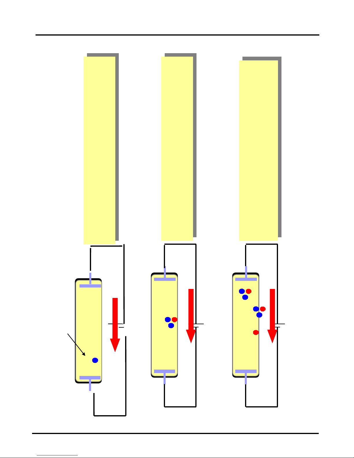
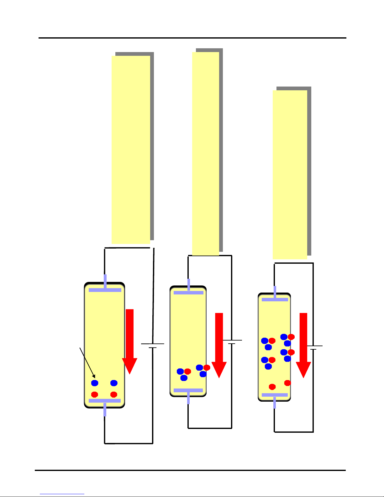
Repeat of α-process and β-process
→ Space insulation break down by
increasing current
→ Discharge
Self-sustained discharge
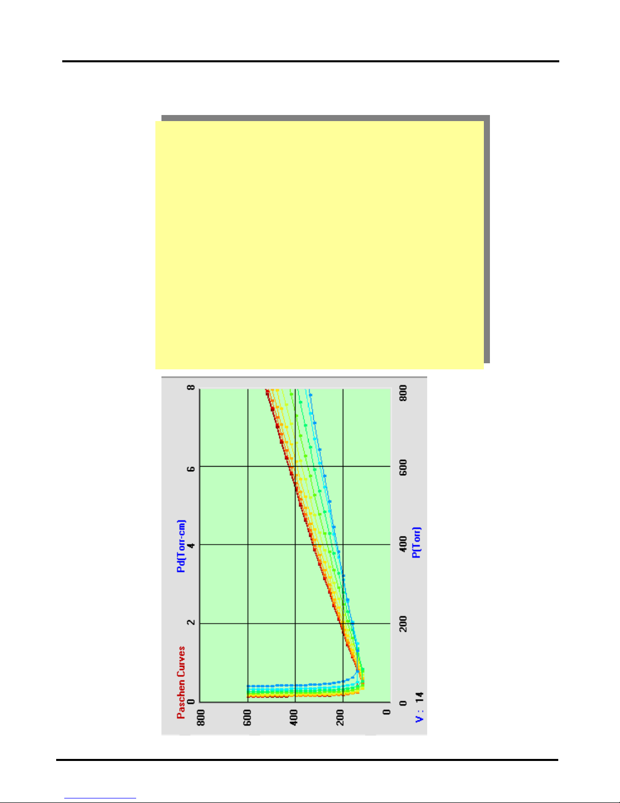
Paschen Curve
- Start voltage of Discharge
(Vf : Minimum voltage for discharge)
display a curve line of pressure
* A function of an electrode distance.
* Discharge Mechanism & Delay
Repeat of α-process and β-process
→ Space insulation break down by
increasing current
→ Discharge
Self-sustained discharge
Paschen Curve
- Start voltage of Discharge
(Vf : Minimum voltage for discharge)
display a curve line of pressure
* A function of an electrode distance.
* Discharge Mechanism & Delay
4-6 Paschen Curve
4-6
Samsung Electronics
Introduction PDP
Introduction PDP
Samsung Electronics 4-7
4-7 Wall Charge
Vw1+Vex
Vw1
X Y
Discharge
Start
Discharge
Start
XY
Vex
0V
0V
Y
X
Vex
XY XY
It is displayed differential discharge characteristics about same pulse by Wall Charge. : enable a picture
V
I
Vf
No
Discharge
No
Discharge
Vex -Vw2
Vw2
XY XY
+++
---
+++
---
+++
---
+++
---
4-8 Samsung Electronics
4-8 Process of sustain discharge
Vex
X Y
Vex
0V
0V
Y
X
X Y
Vw1+Vex
X Y
Vw1
Vex
0V
0V
X
Y
X Y
Vex-Vw2
Vw2
X Y
Vw2+Vex
Vex
X Y
Make wall charge
Make wall charge
Input electric field
Input electric field
Discharge
Discharge
Sustain discharge
Sustain discharge
Extinction of discharge
(Wall charge Shield)
Make wall charge
Extinction of discharge
(Wall charge Shield)
Make wall charge
Input electric field
Input electric field
Discharge
Discharge
Sustain discharge
Sustain discharge
+++
---
+++
---
-
-
+
+
+
-
-
+
+
+
++
+
---
+++
---
Introduction PDP
Introduction PDP
Samsung Electronics 4-9
4-9 1Sub-field Image Process - ADS
Reset
Reset
Address
Address
Sustain
Sustain
Function
Sustain Erase
W all Charge Set
Issue
Operation margi n
Contrast
Short Time
Function
S
us tain Erase
Wall Charge Set
Issue
Operation margin
Contrast
Short Time
Function
Select On Cell
Issue
High Speed
Low Voltage
Low Failure
Function
Select On Cell
Issue
High Speed
L
ow Voltage
Low Failure
Function
Discharge On Cell
Issue
H igh Efficiency
Low V oltage
ERC Performance
Function
Discharge On Cell
Issue
High Efficiency
Low Voltage
ERC Performance
.
.
.
.
.
.
.
.
.
.
.
.
.
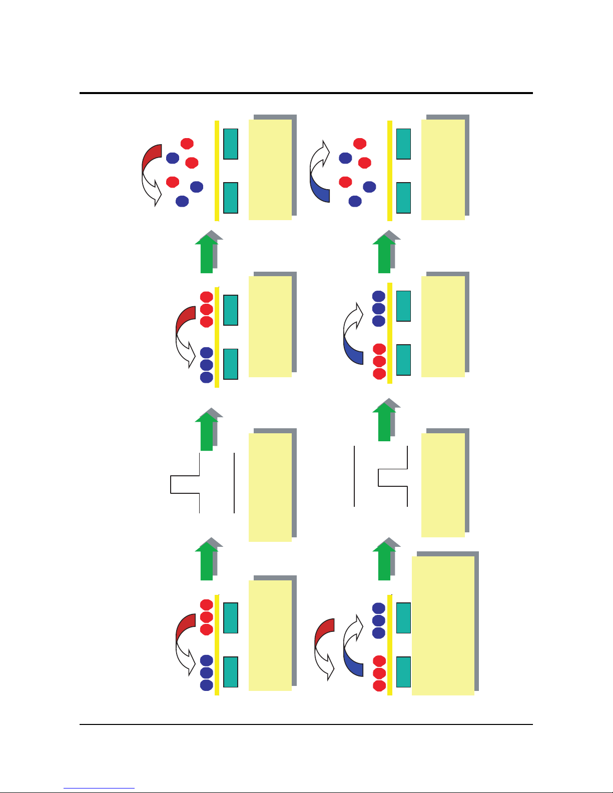
4-10 1 Sub-field Precess - Reset
4-10 Samsung Electronics
4-11 1Sub-field Process - Address 1
4-12 1Sub-field Process - Address 2
Introduction PDP
Introduction PDP
Samsung Electronics 4-11
4-13 1Sub-field Process - Address 3
4-14 1Sub-field Process - Address 4
Introduction PDP
4-12 Samsung Electronics
4-15 1Sub-field Process - Address 5
4-16 1Sub-field Process - Address 6
Introduction PDP
Samsung Electronics 4-13
4-17 1Sub-field Process - Address 7
4-18 1Sub-field Process - Address 8
Introduction PDP
4-14 Samsung Electronics
4-20 1Sub-field Process - Sustain
4-19 1Sub-field Process - Address 9
Introduction PDP
Samsung Electronics 4-15
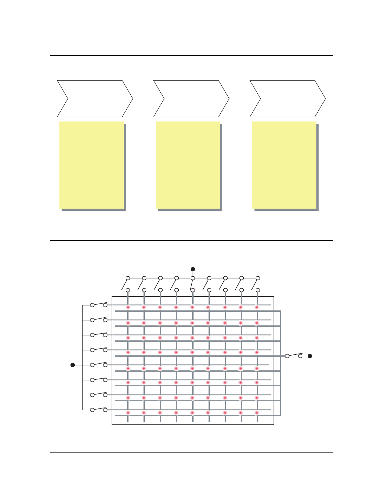
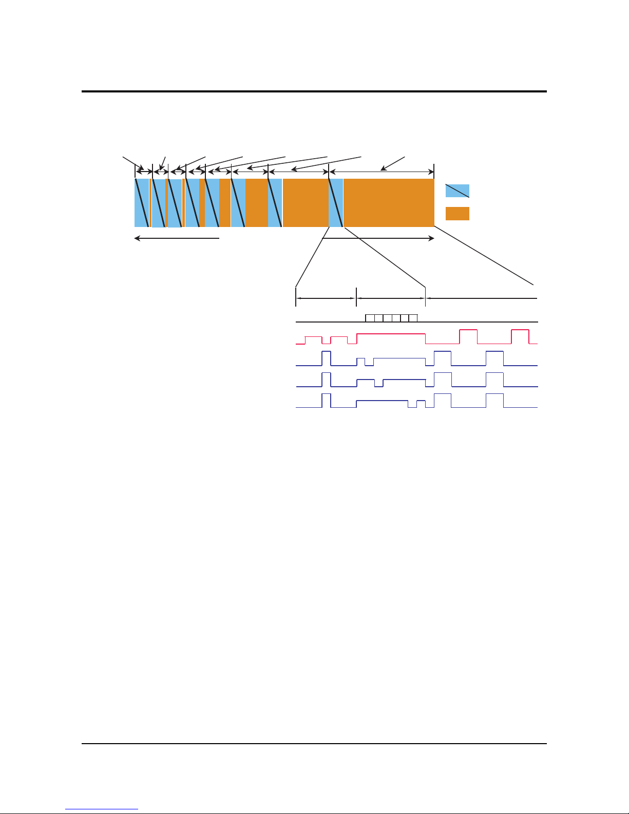
4-21 Frame Structure - ADS
SF1 SF2 SF3 SF4 SF5 SF6 SF7 SF8
1
..
...
2
480
128T64T32T16T8T4T2T1T
1TV field (time)
scan line
address
sustain
sub-field
Reset
Period
Address
Period
Sustain
Period
X
Y1
Y2
Yn
D
SF1 SF2 SF3 SF4 SF5 SF6 SF7 SF8
O
r
i
g
i
n
a
l
I
m
a
g
e
1
..
...
2
480
128T64T32T16T8T4T2T1T
1TV field (time)
scan line
address
sustain
sub-field
Introduction PDP
4-22 Picture Structure by 8 sub-field
4-16
Samsung Electronics

Introduction PDP
Samsung Electronics 4-17
Reset Period
Sustain elimination discharge
a. Very thin Pulse elimination method
b. full width Pulse elimination method
c. Self-erase elimination method
d. Infirm discharge elimination method
Wall Charge Set-up for Address
: Actually, made wall charge profit of Ramp or RC pulse by infirm discharge
Contrast
: To make Back Ground bright interference Contrast
Drive Margin
.
.
.
.
Address Period
Based action : An address electrode and with a Y-electrode between generate discharge,
Selected cell and not selected cell by Sustain Pulse have different
characteristic with wall charge
Write Address / Erase Address
Non Address Failure
: Address Pulse -Scan Pulse potential difference & Scan width a design
High speed Addressing
: It is important technique for high resolution, high brightness, low cost
Discharge delay reduction by discharge condition improvement and drive waveform
Low voltage Address
: It is profitable of cost down by reduce resisting pressure Driver IC.
.
.
.
Sustain Period
Pulse form
: Input alternation pulse to X-electrode and Y-electrode
Reality picture realizable sustain discharge
: It is decide sustain discharge of wall charge difference separated with a cell between
by address discharge
Sustain drive Margin
a. Drive of sustain discharge : decided by Panel s Vs value
b. The first stage drive : Reset discharge / Made Wall Charge selectivity by Address
discharge and panel s Vf
Efficiency improve
: It is many power consumption and need efficiency improve in Sustain discharge
.
.
Introduction PDP
4-18 Samsung Electronics
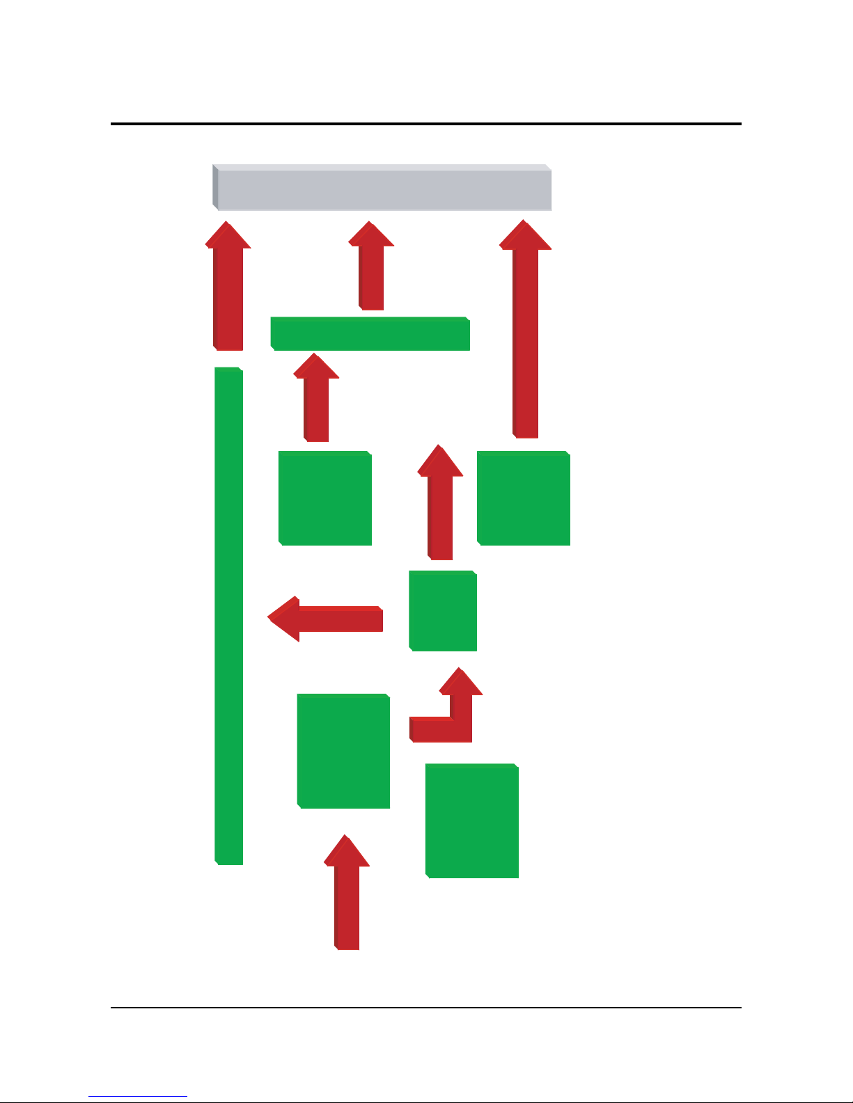
4-23 PDP Drive Set
Address Buffer Board
Address Buffer Board
Y Driver
Y Driver
Board
Board
Power
Supply
Board
Logic
Board
Image
Image
Processing
Processing
Board
Board
Scan Buffer Board
Scan Buffer Board
Image signal source
X, Y Control signal
Address Data signal
RGB & Sync & Clock
Y-output
Scan power
Scan signal
Y-output
Scan P
ulse
X-output
Address
output
Port of Pa nel Electrode
Port of Panel Electrode
X Driver
X Driver
Board
Board
Input : AC Power common in use
Output : All voltages of each B’ds
Introduction PDP
Samsung Electronics 4-19
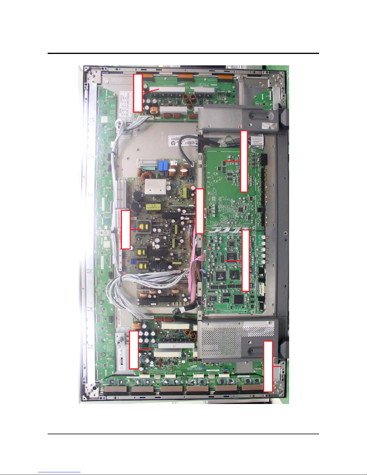
SMPS
X-BOARD
PCB-CONTROL
Y-BOARD
DIGITAL BOARD
LOGIC-BOARD
ANALOG BOARD
4-24 PCB

4-20 Samsung Electronics
MEMO
 Loading...