

Samsung BL8531H User Manual
12BIT 10MSPS ADC BL8531H_ADC
GENERAL DESCRIP TION FEATURES
The BL8531H_ADC is a CMOS 12bit analog-to-digital
converter (ADC). It converts the analog input signal
into 12bit binary digital codes at a maximum
sampling rate of 10MHz.
The device is a monolithic ADC with an on-chip,
high-performanc e, s ample-and-hold Amplifie r (SHA)
and current referenc. The structure allows both
differential and single -ended input.
This 12bit ADC has also 3 channel MUX, so 3
channel inputs are accepta ble.
TYPICAL APP LICATIONS
CCD Imaging (Copiers, Scanners, Cameras)
Medical Instrum ents
Digital Communication Systems
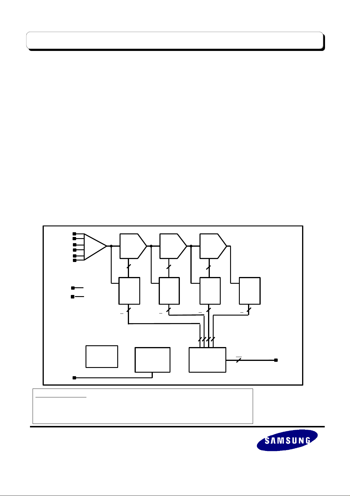
FUNCTIONAL BLOCK DIAGRAM
3CH.
Analog
Inputs
SHA
MDAC
1
MDAC
Resolution : 12bit
-
Maximum Conversion Rate : 10MHz
-
Power Supply : 5V
-
Power Consumption : 100mW (typic al)
-
Reference Volta ge : 3.5V, 1.5V (dual reference)
-
Input Range : 0.5V ~ 4.5V (4.0V
-
Differential Linearity Error : ±0.7 LSB
-
Integral Linearity Error : ±1.0 LSB
-
Signal to Noise & Distortion Ratio : 65dB
-
Total Ha rmonic Distortion : 74dB
-
)
P-P
- 3 Channel Inputs
Digital Output : CMOS Level
-
Opera ting Temperature Range : 0ºC ~ 70ºC
-
MDAC
2
3
Refe rence
Input
Main
Bia s
FLASH
1
4
CLOCK
GEN.
FLASH
2
3
FLASH
3
3 3
DIGITAL
LOGIC
FLASH
12
Clock
Ver 1.1 (Apr. 2002)
No responsibility is assum ed by SEC for its use nor for any infringements of patents
or other rights of third parties that may result from its use. The content of this
data sheet is subject to change without any notice.
SAMSUNG ELECTRONICS Co. LTD
4
Digital
Output
12BIT 10MSPS ADC
CORE PIN DESCRIPTION
BL8 5 3 1 H_ADC
NAME I/O TYPE I/O PAD PIN DESCRIPTION
REFTOP AO poar10_bb Reference Top Forc e (3.5V)
REFBOT AO poar10_bb Reference Bottom Force (1.5V)
CML AO poar10_bb Internal Bia s
VDDA AP vdda Ana log Power (5V)
VBB AG vbba Analog Sub Bias
VSSA AG vssa Ana log Ground
R_INP AI piar10_bb
R_INN AI piar10_bb
G_INP AI pia r10_b
G_INN AI piar10_bb
B_INP AI piar10_bb
B_INN AI piar10_bb
REDB DI pic c_bb RED Channel Select (0:select)
GRE ENB DI picc_bb GREEN Channel Select (0:select)
BLUEB DI pic c_bb BLUE Channel Select (0:select)
STBY DI pic c_bb
CKIN DI picc_bb Sampling Clock Input
D[11:0] DO pot4_bb Digital Output
VSSD DG vssd Digital GND
VDDD DP vddd Digital Power (5V)
Ana log Input (RED) +
(Input Range : 1.5V ~ 3.5V)
Ana log Input (RED) (Input Range : 1.5V ~ 3.5V)
Ana log Input (GREEN) +
(Input Range : 1.5V ~ 3.5V)
Ana log Input (GREEN) (Input Range : 1.5V ~ 3.5V)
Ana log Input (BLUE) +
(Input Range : 1.5V ~ 3.5V)
Ana log Input (BLUE) (Input Range : 1.5V ~ 3.5V)
VDD=power saving (standby),
GND=normal
vdda vssa vbb vddd
I/O TYPE ABBR.
-AI : Analog Input
-DI : Digital Input
-AO : Analog Output
-DO : Analog Output
-AP : Analog Power
-AG : Analog Ground
-DP : Digital Power
-DG : Digital Ground
-AB : Ana log Bidirection
-DB : Digital Bidirection
vssd
R_INP
R_INN
G_INP
G_INN
B_INP
B_INN
SEC ASIC
REFTOP
bl8531h_ad c
REFBOT
2 / 11
CML
STBY CKIN
¢¸ REDB
¢¸ GREENB
¢¸ BLUEB
[MSB:L SB]
D[11:0]
MIXED
12BIT 10MSPS ADC
BL8 5 3 1 H_ADC
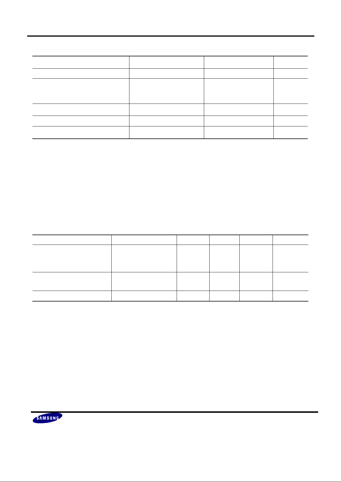
ABSOLUTE MAXIMUM RATINGS
Characteristics Sym bol Value Unit
Supply Voltage VDD 6.0 V
R_INP/R_INN
Analog Input Voltage
Digital Input Voltage CLK VSS to VDD V
G_INP/G_INN
B_INP/B_INN
VSS to VDD V
Storage Temperature Range Tstg -45 to 150
Operating Tempe rature Range Topr 0 to 70
NOTES
1. Absolute ma ximum rating specifies the values beyond which the device may be damaged permanently. Exposure to
ABSOLUTE MAXIMUM RATING conditions for extended periods may affect reliability. Each condition value is
applie d with the other values kept within the following operating conditions and func tion opera tion under any of these
conditions is not implied.
2. All voltages are measured with respect to VSS unles s otherwise specif ie d.
3. 100pF capac itor is discha rged through a 1.5kΩresistor (Human body model)
RECOMMENDED OPERATI NG CONDITIONS
Chara cteristics Symbol Min Typ Max Unit
VDDA1
Supply Voltage
Analog Input Voltage
VDDA2
VDDA3
R_INP/G_INP/B_INP
R_INN/G_INN/B_INN
4.75 5.0 5.25 V
0.5 -
2.5
4.5
ºC
ºC
V
Operating Temperature Toper 0 - 70
NOTES
It is strongly recommended that all the supply pins (VDDA, VDDD) be powered from the same source to avoid power
latch- up.
SEC ASIC
3 / 11
ºC
MIXED
12BIT 10MSPS ADC
BL8 5 3 1 H_ADC
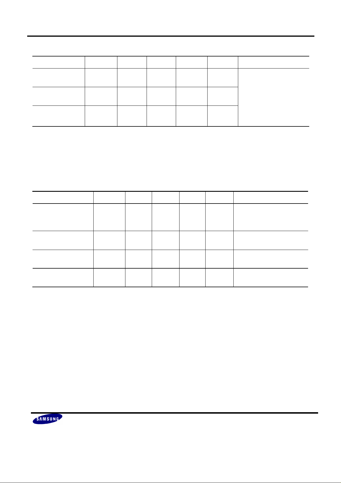
DC ELECTRICAL CHARACTERISTICS
Chara cteristics Symbol Min Typ Max Unit Test Condition
Differential
Nonlinearity
Integral
Nonlinearity
Offset
Voltage
(Converter Spe c ific ati ons : VDDA=VDDD=5V, VSSA=VSSD=0V,
Toper=25°C, REFTOP=3.5V, REFBOT=1.5V unless otherwi se specified)
DNL -
INL -
OFF - 10 - mV
0.7
±
1.0 - LSB
±
1 LSB
±
REFTOP=3.5V
REFBOT =1.5V
AC ELECTRICAL CHARACTE RISTICS
Chara cteristics Symbol M i n Typ Max Unit Test Condition
Maximum
Conversion Rate
Dynamic Supply
Current
fc - 10 MHz
IVDD - 20 mA
AINR=R_INP-R_INN
AING=G_INP-G_INN
AING=B_INP-B_INN
(without system load)
fc=10MHz
Signal-to-Noise &
Distortion Ratio
Total Harmonic
Distortion
(Conversion Specifications : VDDA=VDDD=5V, VSSA=VSSD=0V,
Toper=25°C, REFTOP=3.5V, REFBOT=1.5V unless otherwise specified)
SEC ASIC
SNDR - 65 - dB
THD - 74 - dB
4 / 11
AIN=1MHz,
Differential Input
AIN=1MHz,
Differential Input
MIXED
 Loading...