


RICOH RH5RH312B-T2, RH5RH313B-T1, RH5RH313B-T2, RH5RH321A-T1, RH5RH321A-T2 Datasheet
...PWM STEP-UP DC/DC CONVERTER
RH5RH××1A/××2B/××3B SERIES
APPLICATION MANUAL
NO.EA-023-0006
PWM STEP-UP DC/DC CONVERTER
RH5RH ××1A/××2B/××3B SERIES
OUTLINE
The RH5RH××1A/××2B/××3B Series are PWM Step-up DC/DC converter ICs by CMOS process.
The RH5RH××1A IC consists of an oscillator, a PWM control circuit, a driver transistor (Lx switch), a reference voltage unit, an error amplifier, a phase compensation circuit, resistors for voltage detection, a soft-start circuit, and an Lx switch protection circuit. A low ripple, high efficiency step-up DC/DC converter can be constructed of this RH5RH××1A IC with only three external components, that is, an inductor, a diode and a capacitor.
These RH5RH××1A/××2B/××3B ICs can achieve ultra-low supply current (no load) –TYP. 15µA –by a newly developed PWM control circuit, equivalent to the low supply current of a VFM (chopper) Step-up DC/DC converter.
Furthermore, these ICs can hold down the supply current to TYP. 2µA by stopping the operation of the oscillator when the input voltage > (the output voltage set value + the dropout voltage by the diode and the inductor).
These RH5RH××1A/××2B/××3B Series ICs are recommendable to the user who desires a low ripple PWM DC/DC converter, but cannot adopt a conventional PWM DC/DC converter because of its too large supply current.
The RH5RH××2B/××3B Series ICs use the same chip as that employed in the RH5RH××1A IC and are provided with a drive pin (EXT) for an external transistor. Because of the use of the drive pin (EXT), an external transistor with a low saturation voltage can be used so that a large current can be caused to flow through the inductor and accordingly a large output current can be obtained. Therefore, these RH5RH××2B/××3B Series ICs are recommendable to the user who need a current as large as several tens mA to several hundreds mA.
The RH5RH××3B IC also includes an internal chip enable circuit so that it is possible to set the standby supply current at MAX. 0.5µA.
These RH5RH××1A/××2B/××3B ICs are suitable for use with battery-powered instruments with low noise and low supply current.
FEATURES
• Small Number of External Components |
.......... |
|
|
|
|||
Only an inductor, a diode and a capacitor (RH5RH××1A) |
|||||||
• Low Supply Current |
........................................... |
|
|
|
|||
|
|
TYP. 15µA (RH5RH301A) |
|||||
• Low Ripple and Low Noise |
|
|
|
.................. |
|
||
• Low Start-up Voltage (when the output current is 1mA) |
MAX. 0.9V |
||||||
|
|||||||
• High Output Voltage Accuracy |
.......................... |
|
|
|
|||
|
±2.5% |
|
|
|
|||
• High Efficiency ...................................................TYP. 85% |
|
||||||
• Low Temperature-Drift Coefficient of Output Voltage |
...................... |
TYP. ±50 ppm/˚C |
|||||
|
|
||||||
• Soft-Start.............................................................MIN. 500µs
• Small Packages...................................................SOT-89 (RH5RH××1A, RH5RH××2B),
SOT-89-5 (RH5RH××3B)
APPLICATIONS
•Power source for battery-powered equipment.
•Power source for cameras, camcorders, VCRs, PDAs, electronic data banks,and hand-held communication equipment.
•Power source for instruments which require low noise and low supply current, such as hand-held audio equipment.
•Power source for appliances which require higher cell voltage than that of batteries used in the appliances.
1

RH5RH
BLOCK DIAGRAM
Lx |
VLX limiter |
Slow start |
Vref |
|
|
OUT |
|
|
|
|
|
Vss |
Buffer |
Phase Comp. |
|
|
|
|
|
|
LxSW |
|
|
|
PWM control |
– |
|
EXT |
|
+ |
|
OSC |
Error Amp. |
|
|
|
|
||
|
Chip Enable |
|
|
CE
Error Amp. (Error Amplifier) has a DC gain of 80dB, and Phase Comp. (Phase Compensation Circuit) provides the frequency characteristics including the 1st pole (fp=0.25Hz) and the zero point (fz=2.5kHz). Furthermore, another zero point (fz=1.0kHz) is also obtained by the resistors and a capacitor connected to the OUT pin.
(Note) Lx Pin ............only for RH5RH××1A and RH5RH××3B EXT Pin .........only for RH5RH××2B and RH5RH××3B CE Pin ...........only for RH5RH××3B
SELECTION GUIDE
In RH5RH Series, the output voltage, the driver, and the taping type for the ICs can be selected at the user's request. The selection can be made by designating the part number as shown below :
|
RH5RH×××× – ×× ← Part Number |
||||
|
} } |
} |
|
||
|
|
↑ |
↑ |
↑ |
|
|
|
a |
b |
c |
|
|
|
|
|
|
|
Code |
|
|
|
|
Description |
|
|
|
|||
a |
|
Setting Output Voltage (VOUT): |
|||
|
Stepwise setting with a step of 0.1V in the range of 2.7V to 7.5V is possible. |
||||
|
|
||||
|
|
|
|||
|
|
Designation of Driver: |
|||
|
|
1A: Internal Lx Tr. Driver (Oscillator Frequency 50kHz) |
|||
b |
|
2B: |
External Tr. Driver (Oscillator Frequency 100kHz) |
||
|
|
3B: Internal Tr./External Tr. (selectively available) (Oscillator Frequency 100kHz, with chip |
|||
|
|
enable function) |
|||
|
|
|
|||
|
|
Designation of Taping Type : |
|||
|
|
Ex. |
SOT-89 |
: T1, T2 |
|
c |
|
|
SOT-89-5 |
: T1, T2 |
|
|
|
(refer to Taping Specifications) |
|||
|
|
“T1” is prescribed as a standard. |
|||
|
|
|
|
|
|
For example, the product with Output Voltage 5.0V, the External Driver (the Oscillator Frequency 100kHz) and Taping Type T1, is designated by Part Number RH5RH502B-T1.
2
RH5RH
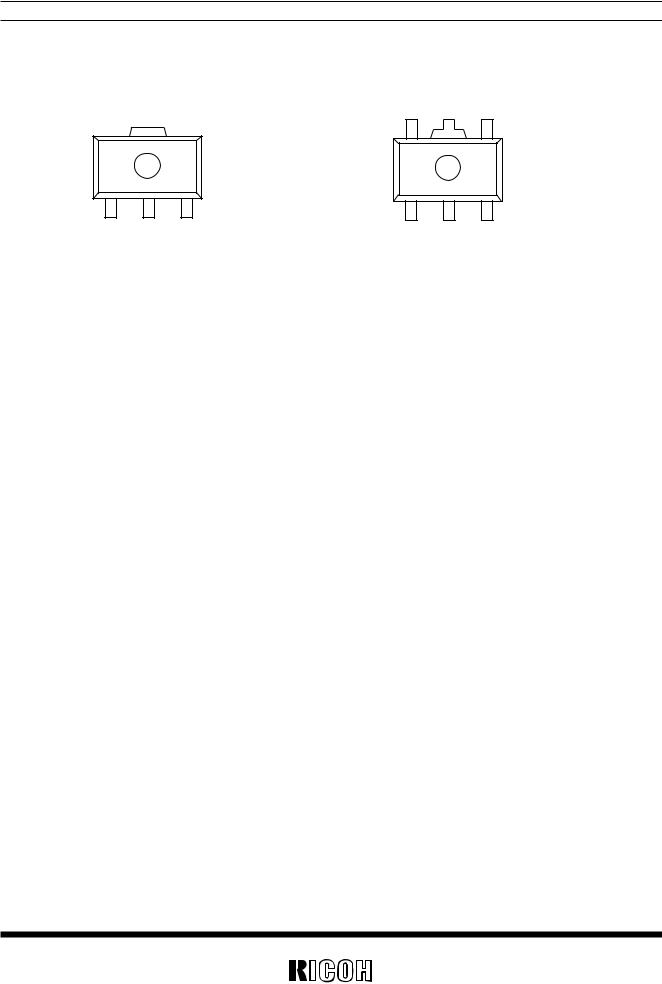
PIN CONFIGURATION
• SOT-89 |
• SOT-89-5 |
|
|
5 |
4 |
|
(mark side) |
|
|
(mark side) |
|
1 |
2 |
3 |
1 |
2 |
3 |
PIN DESCRIPTION
|
Pin No. |
|
|
|
|
|
|
|
|
|
Symbol |
Description |
|||
××1B |
××2B |
××3B |
|||||
|
|
|
|
||||
|
|
|
|
|
|
|
|
1 |
1 |
5 |
VSS |
Ground Pin |
|||
|
|
|
|
|
|
|
|
2 |
2 |
2 |
OUT |
Step-up Output Pin, Power Supply (for device itself) |
|||
|
|
|
|
|
|
|
|
3 |
— |
4 |
|
Lx |
Switching Pin (Nch Open Drain) |
||
|
|
|
|
|
|
|
|
— |
3 |
3 |
EXT |
External Tr. Drive Pin (CMOS Output) |
|||
|
|
|
|
|
|
|
|
— |
— |
1 |
|
Chip Enable Pin (Active Low) |
|||
|
CE |
|
|||||
|
|
|
|
|
|
|
|
3
RH5RH
ABSOLUTE MAXIMUM RATINGS |
|
|
Vss=0V |
|||||
|
|
|
|
|
|
|
|
|
Symbol |
|
|
Item |
|
Rating |
Unit |
Note |
|
|
|
|
|
|
|
|
|
|
VOUT |
Output Pin Voltage |
|
+12 |
V |
|
|
||
|
|
|
|
|
|
|
|
|
VLX |
Lx Pin Voltage |
|
+12 |
V |
Note1 |
|
||
|
|
|
|
|
|
|
|
|
VEXT |
EXT Pin Voltage |
|
– 0.3 to VOUT+0.3 |
V |
Note2 |
|
||
|
|
|
|
|
|
|
|
|
|
|
|
|
|
|
|
|
|
VCE |
CE Pin Voltage |
|
–0.3 to VOUT+0.3 |
V |
Note3 |
|
||
|
|
|
|
|
|
|
|
|
ILX |
Lx Pin Output Current |
|
250 |
mA |
Note1 |
|
||
|
|
|
|
|
|
|
|
|
IEXT |
EXT Pin Current |
|
±50 |
mA |
Note2 |
|
||
|
|
|
|
|
|
|
|
|
PD |
Power Dissipation |
|
500 |
mW |
|
|
||
|
|
|
|
|
|
|
|
|
Topt |
Operating Temperature Range |
|
–30 to +80 |
˚C |
|
|
||
|
|
|
|
|
|
|
|
|
Tstg |
Storage Temperature Range |
|
–55 to +125 |
˚C |
|
|
||
|
|
|
|
|
|
|
|
|
Tsolder |
Lead Temperature(Soldering) |
|
260˚C,10s |
|
|
|
||
|
|
|
|
|
|
|
|
|
(Note 1) |
Applicable to RH5RH |
××1A and RH5RH××3B. (Note 2) Applicable to RH5RH××2B and RH5RH××3B. |
(Note 3) |
Applicable to RH5RH |
××3B. |
ABSOLUTE MAXIMUM RATINGS
Absolute Maximum ratings are threshold limit values that must not be exceeded even for an instant under any conditions. Moreover, such values for any two items must not be reached simultaneously. Operation above these absolute maximum ratings may cause degradation or permanent damage to the device. These are stress ratings only and do not necessarily imply functional operation below these limits.
4

|
|
|
|
|
|
|
|
|
RH5RH |
||
ELECTRICAL CHARACTERISTICS |
|
|
|
|
|
|
|
||||
• RH5RH301A |
|
|
|
|
|
|
VOUT=3.0V |
||||
|
|
|
|
|
|
|
|
|
|||
|
|
|
|
|
|
|
|
|
|
|
|
|
Symbol |
|
Item |
Conditions |
MIN. |
TYP. |
MAX. |
Unit |
|
Note |
|
|
|
|
|
|
|
|
|
|
|
|
|
|
VOUT |
|
Output Voltage |
|
2.925 |
3.000 |
3.075 |
V |
|
|
|
|
|
|
|
|
|
|
|
|
|
|
|
|
VIN |
|
Input Voltage |
|
|
|
8 |
V |
|
|
|
|
|
|
|
IOUT=1mA,VIN : 0→2V |
|
|
|
|
|
|
|
|
Vstart |
|
Start-up Voltage |
|
0.8 |
0.9 |
V |
|
|
|
|
|
|
|
|
IOUT=1mA,VIN : 2→0V |
|
|
|
|
|
|
|
|
Vhold |
|
Hold-on Voltage |
0.7 |
|
|
V |
|
|
|
|
|
|
|
|
To be measured at OUT Pin |
|
|
|
|
|
|
|
|
IDD1 |
|
Supply Current 1 |
|
15 |
25 |
µA |
|
|
|
|
|
|
(excluding Switching Current) |
|
|
|
|
|||||
|
|
|
|
|
|
|
|
|
|
|
|
|
|
|
|
To be measured at OUT Pin |
|
|
|
|
|
|
|
|
|
|
|
|
|
|
|
|
|
|
|
|
IDD2 |
|
Supply Current 2 |
(excluding Switching Current) |
|
2 |
5 |
µA |
|
|
|
|
|
|
|
VIN=3.5V |
|
|
|
|
|
|
|
|
|
|
|
|
|
|
|
|
|
|
|
|
ILX |
|
Lx Switching Current |
VLX=0.4V |
60 |
|
|
mA |
|
|
|
|
|
|
|
|
|
|
|
|
|
|
|
|
ILXleak |
|
Lx Leakage Current |
VLX=6V,VIN=3.5V |
|
|
0.5 |
µA |
|
|
|
|
|
|
|
|
|
|
|
|
|
|
|
|
fosc |
|
Oscillator Frequency |
|
40 |
50 |
60 |
kHz |
|
|
|
|
|
|
|
|
|
|
|
|
|
|
|
|
Maxdty |
|
Oscillator Maximum Duty |
on (VLX “L” ) side |
70 |
80 |
90 |
% |
|
|
|
|
|
Cycle |
|
|
|
||||||
|
|
|
|
|
|
|
|
|
|
|
|
|
|
|
|
|
|
|
|
|
|
|
|
|
η |
|
Efficiency |
|
70 |
85 |
|
% |
|
|
|
|
|
|
|
Time required for the rising |
|
|
|
|
|
|
|
|
tstart |
|
Soft-Start Time |
0.5 |
2.0 |
|
ms |
|
Note1 |
|
|
|
|
of VOUT up to 3V. |
|
|
|
||||||
|
|
|
|
|
|
|
|
|
|
|
|
|
|
|
|
|
|
|
|
|
|
|
|
|
VLXlim |
|
VLX Voltage Limit |
Lx Switch ON |
0.65 |
0.8 |
1.0 |
V |
|
Note2 |
|
|
|
|
|
|
|
|
|
|
|
|
|
Unless otherwise provided, VIN=1.8V, VSS=0V, IOUT=10mA, Topt=25˚C, and use External Circuit of Typical
Application (FIG. 1).
(Note 1) Soft-Start Circuit is operated in the following sequence :
(1)VIN is applied.
(2)The voltage (Vref) of the reference voltage unit is maintained at 0V for about 200µs after the application of VIN.
(3)The output of Error Amp. is raised to “H” level during the maintenance of the voltage (Vref) of the reference voltage unit.
(4)After the rise of Vref, the output of Internal Error Amp. is gradually decreased to an appropriate value by the function of Internal Phase Compensation Circuit, and the Output Voltage is gradually increased in accordance with the gradual decrease of the output of Internal Error Amp.
(Note 2) ILX is gradually increased after Lx Switch is turned ON. In accordance with the increase of ILX, VLX is also increased. When VLX reaches VLXlim, Lx Switch is turned OFF by an Lx Switch Protection Circuit.
5
RH5RH |
|
|
|
|
|
|
|
|
|
||
|
• RH5RH501A |
|
|
|
|
|
|
VOUT=5.0V |
|||
|
|
|
|
|
|
|
|
|
|||
|
|
|
|
|
|
|
|
|
|
|
|
|
Symbol |
|
Item |
Conditions |
MIN. |
TYP. |
MAX. |
Unit |
|
Note |
|
|
|
|
|
|
|
|
|
|
|
|
|
|
VOUT |
|
Output Voltage |
|
4.875 |
5.000 |
5.125 |
V |
|
|
|
|
|
|
|
|
|
|
|
|
|
|
|
|
VIN |
|
Input Voltage |
|
|
|
8 |
V |
|
|
|
|
|
|
|
Iout=1mA,Vin:0→2V |
|
|
|
|
|
|
|
|
Vstart |
|
Start-up Voltage |
|
0.8 |
0.9 |
V |
|
|
|
|
|
|
|
|
Iout=1mA,Vin:2→0V |
|
|
|
|
|
|
|
|
Vhold |
|
Hold-on Voltage |
0.7 |
|
|
V |
|
|
|
|
|
|
|
|
To be measured at OUT Pin |
|
|
|
|
|
|
|
|
IDD1 |
|
Supply Current 1 |
|
30 |
45 |
µA |
|
|
|
|
|
|
(excluding Switching Current) |
|
|
|
|
|||||
|
|
|
|
|
|
|
|
|
|
|
|
|
|
|
|
To be measured at OUT Pin |
|
|
|
|
|
|
|
|
|
|
|
|
|
|
|
|
|
|
|
|
IDD2 |
|
Supply Current 2 |
(excluding Switching Current) |
|
2 |
5 |
µA |
|
|
|
|
|
|
|
VIN=5.5V |
|
|
|
|
|
|
|
|
|
|
|
|
|
|
|
|
|
|
|
|
ILX |
|
Lx Switching Current |
VLX=0.4V |
80 |
|
|
mA |
|
|
|
|
|
|
|
|
|
|
|
|
|
|
|
|
ILXleak |
|
Lx Leakage Current |
VLX=6V,VIN=5.5V |
|
|
0.5 |
µA |
|
|
|
|
|
|
|
|
|
|
|
|
|
|
|
|
fosc |
|
Oscillator Frequency |
|
40 |
50 |
60 |
kHz |
|
|
|
|
|
|
|
|
|
|
|
|
|
|
|
|
Maxdty |
|
Oscillator Maximum Duty |
on (VLX “L” ) side |
70 |
80 |
90 |
% |
|
|
|
|
|
Cycle |
|
|
|
||||||
|
|
|
|
|
|
|
|
|
|
|
|
|
|
|
|
|
|
|
|
|
|
|
|
|
η |
|
Efficiency |
|
70 |
85 |
|
% |
|
|
|
|
|
|
|
Time required for the rising |
|
|
|
|
|
|
|
|
tstart |
|
Soft-Start Time |
0.5 |
2.0 |
|
ms |
|
Note1 |
|
|
|
|
of VOUT up to 5V. |
|
|
|
||||||
|
|
|
|
|
|
|
|
|
|
|
|
|
|
|
|
Lx Switch ON |
0.65 |
0.8 |
1.0 |
V |
|
Note2 |
|
|
VLXlim |
|
VLX Voltage Limit |
|
|
||||||
|
|
|
|
|
|
|
|
|
|
|
|
Unless otherwise provided, VIN=3V, Vss=0V, IOUT=10mA, Topt=25˚C, and use External Circuit of Typical
Application (FIG. 1).
(Note 1) Soft-Start Circuit is operated in the following sequence :
(1)VIN is applied.
(2)The voltage (Vref) of the reference voltage unit is maintained at 0V for about 200µs after the application of VIN.
(3)The output of Error Amp. is raised to “H” level during the maintenance of the voltage (Vref) of the reference voltage unit.
(4)After the rise of Vref, the output of Internal Error Amp. is gradually decreased to an appropriate value by the function of Internal Phase Compensation Circuit, and the Output Voltage is gradually increased in accordance with the gradual decrease of the output of Internal Error
Amp.
(Note 2) ILX is gradually increased after Lx Switch is turned ON. In accordance with the increase of ILX, VLX is also increased. When VLX reaches VLXlim, Lx Switch is turned OFF by an Lx Switch Protection Circuit.
6

|
|
|
|
|
|
|
|
RH5RH |
||
• RH5RH302B |
|
|
|
|
|
|
VOUT=3.0V |
|||
|
|
|
|
|
|
|
|
|
|
|
Symbol |
|
Item |
Conditions |
MIN. |
TYP. |
MAX. |
Unit |
|
Note |
|
|
|
|
|
|
|
|
|
|
|
|
VOUT |
|
Output Voltage |
|
2.925 |
3.000 |
3.075 |
V |
|
|
|
|
|
|
|
|
|
|
|
|
|
|
VIN |
|
Input Voltage |
|
|
|
8 |
V |
|
|
|
|
|
|
EXT no load,VOUT :0→2V |
|
|
|
|
|
|
|
Vstart |
|
Oscillator Start-up Voltage |
|
0.7 |
0.8 |
V |
|
|
|
|
|
|
|
|
|
|
|
|
|
|
|
IDD1 |
|
Supply Current 1 |
EXT no load,VOUT=2.88V |
|
30 |
50 |
µA |
|
|
|
|
|
|
|
|
|
|
|
|
|
|
IDD2 |
|
Supply Current 2 |
EXT no load,VOUT=3.5V |
|
2 |
5 |
µA |
|
|
|
|
|
|
|
|
|
|
|
|
|
|
IEXTH |
|
EXT “H” Output Current |
VEXT=VOUT–0.4V |
|
|
–1.5 |
mA |
|
|
|
|
|
|
|
|
|
|
|
|
|
|
IEXTL |
|
EXT “L” Output Current |
VEXT=0.4V |
1.5 |
|
|
mA |
|
|
|
|
|
|
|
|
|
|
|
|
|
|
fosc |
|
Oscillator Frequency |
|
80 |
100 |
120 |
kHz |
|
|
|
|
|
|
|
|
|
|
|
|
|
|
Maxdty |
|
Oscillator Maximum Duty |
VEXT “H” side |
70 |
80 |
90 |
% |
|
|
|
|
Cycle |
|
|
|
||||||
|
|
|
|
|
||||||
|
|
|
|
|
|
|
|
|
|
|
|
|
|
Time required for the rising |
|
|
|
|
|
|
|
tstart |
|
Soft-Start Time |
0.5 |
2.0 |
|
ms |
|
Note1 |
|
|
|
|
|
of VOUT up to 3V |
|
|
|
|
|
|
|
|
|
|
|
|
|
|
|
|
|
|
Unless otherwise provided, VIN=1.8V, Vss=0V, IOUT=10mA, Topt=25˚C, and use External Circuit of Typical
Application (FIG. 2).
• RH5RH502B
VOUT=5.0V
Symbol |
Item |
Conditions |
MIN. |
TYP. |
MAX. |
Unit |
Note |
|
|
|
|
|
|
|
|
VOUT |
Output Voltage |
|
4.875 |
5.000 |
5.125 |
V |
|
|
|
|
|
|
|
|
|
VIN |
Input Voltage |
|
|
|
8 |
V |
|
|
|
EXT no load,VOUT :0→2V |
|
|
|
|
|
Vstart |
Oscillator Start-up Voltage |
|
0.7 |
0.8 |
V |
|
|
|
|
|
|
|
|
|
|
IDD1 |
Supply Current 1 |
EXT no load,VOUT=4.8V |
|
60 |
90 |
µA |
|
|
|
|
|
|
|
|
|
IDD2 |
Supply Current 2 |
EXT no load,VOUT=5.5V |
|
2 |
5 |
µA |
|
|
|
|
|
|
|
|
|
IEXTH |
EXT “H” Output Current |
VEXT=VOUT–0.4V |
|
|
–2 |
mA |
|
|
|
|
|
|
|
|
|
IEXTL |
EXT “L” Output Current |
VEXT=0.4V |
2 |
|
|
mA |
|
|
|
|
|
|
|
|
|
fosc |
Oscillator Frequency |
|
80 |
100 |
120 |
kHz |
|
|
|
|
|
|
|
|
|
Maxdty |
Oscillator Maximum Duty |
VEXT “H” side |
70 |
80 |
90 |
% |
|
Cycle |
|
||||||
|
|
||||||
|
|
|
|
|
|
|
|
|
|
Time required for the rising |
|
|
|
|
|
tstart |
Soft-Start Time |
0.5 |
2.0 |
|
ms |
Note1 |
|
of VOUT up to 5V |
|
||||||
|
|
|
|
|
|
|
|
|
|
|
|
|
|
|
|
Unless otherwise provided, VIN=3V, Vss=0V, IOUT=10mA, Topt=25˚C and use External Circuit of Typical Application (FIG. 2).
(Note 1) refer to page 5 (Note 1)
7

RH5RH |
|
|
|
|
|
|
|
|
|
|
|
|
|
|
|
|
|
||
• RH5RH303B |
|
|
|
|
|
|
|
|
|
|
|
|
|
|
VOUT=3.0V |
||||
|
|
|
|
|
|
|
|
|
|
|
|
|
|
|
|
|
|||
|
|
|
|
|
|
|
|
|
|
|
|
|
|
|
|
|
|
|
|
|
Symbol |
|
|
|
|
|
Item |
Conditions |
MIN. |
TYP. |
MAX. |
Unit |
|
Note |
|
||||
|
|
|
|
|
|
|
|
|
|
|
|
|
|
|
|
|
|
|
|
|
VOUT |
|
Output Voltage |
|
|
|
|
|
2.925 |
3.000 |
3.075 |
V |
|
|
|
||||
|
|
|
|
|
|
|
|
|
|
|
|
|
|
|
|
|
|
|
|
|
VIN |
|
Input Voltage |
|
|
|
|
|
|
|
8 |
V |
|
|
|
||||
|
|
|
|
|
|
|
|
IOUT=1mA,VIN : 0→2V |
|
|
|
|
|
|
|
||||
|
Vstart |
|
Start-up Voltage |
|
0.8 |
0.9 |
V |
|
|
|
|||||||||
|
|
|
|
|
|
|
|
|
|
|
|
|
|
|
|
|
|
|
|
|
Vhold |
|
Hold-on Voltage |
IOUT=1mA,VIN : 2→0V |
0.7 |
|
|
V |
|
|
|
||||||||
|
|
|
|
|
|
|
|
|
|
|
|
|
|
|
|
|
|
|
|
|
η |
|
Efficiency |
|
|
|
|
|
70 |
85 |
|
% |
|
|
|
||||
|
|
|
|
|
|
|
|
|
|
|
|
|
|
|
|
|
|
|
|
|
IDD1 |
|
Supply Current 1 |
To be measured at OUT pin |
|
30 |
50 |
µA |
|
|
|
||||||||
|
|
|
|
|
|
|
|
|
|
|
|
|
|
|
|
|
|
|
|
|
IDD2 |
|
Supply Current 2 |
To be measured at OUT pin |
|
2 |
5 |
µA |
|
|
|
||||||||
|
|
VIN=3.5V |
|
|
|
|
|||||||||||||
|
|
|
|
|
|
|
|
|
|
|
|
|
|
|
|||||
|
|
|
|
|
|
|
|
VLX=0.4V |
60 |
|
|
mA |
|
|
|
||||
|
ILX |
|
Lx Switching Current |
|
|
|
|
|
|||||||||||
|
|
|
|
|
|
|
|
|
|
|
|
|
|
|
|
|
|
|
|
|
ILXleak |
|
Lx Leakage Current |
VLX=6V,VIN=3.5V |
|
|
0.5 |
µA |
|
|
|
||||||||
|
|
|
|
|
|
|
|
|
|
|
|
|
|
|
|
|
|
|
|
|
IEXTH |
|
EXT “H” Output Current |
VEXT=VOUT–0.4V |
|
|
–1.5 |
mA |
|
|
|
||||||||
|
|
|
|
|
|
|
|
|
|
|
|
|
|
|
|
|
|
|
|
|
IEXTL |
|
EXT “L” Output Current |
VEXT=0.4V |
1.5 |
|
|
mA |
|
|
|
||||||||
|
|
|
|
|
|
|
|
|
|
|
|
|
|
|
|
|
|
|
|
|
|
|
|
|
|
|
|
VOUT≥1.5V |
VOUT–0.4 |
|
|
V |
|
|
|
||||
|
VCEH1 |
|
CE “H” Level 1 |
|
|
|
|
|
|||||||||||
|
|
|
|
|
|
|
|
|
|
|
|
|
|
|
|
|
|
|
|
|
|
|
|
|
|
|
|
VOUT≥1.5V |
|
|
0.4 |
V |
|
|
|
||||
|
VCEL1 |
|
CE “L” Level 1 |
|
|
|
|
|
|||||||||||
|
|
|
|
|
|
|
|
|
|
|
|
|
|
|
|
|
|
|
|
|
|
|
|
|
|
|
|
0.8V≤ VOUT<1.5V |
VOUT–0.1 |
|
|
V |
|
|
|
||||
|
VCEH2 |
|
CE “H” Level 2 |
|
|
|
|
|
|||||||||||
|
|
|
|
|
|
|
|
0.8V≤ VOUT<1.5V |
|
|
0.1 |
V |
|
|
|
||||
|
VCEL2 |
|
|
|
|
“L” Level 2 |
|
|
|
|
|
||||||||
|
|
|
CE |
|
|
|
|
|
|
|
|||||||||
|
|
|
|
|
|
|
|
|
|
|
|
|
|
|
0.5 |
µA |
|
|
|
|
|
|
|
|
|
|
|
|
|
|
|
|
|
|
|
|
|||
|
ICEH |
|
CE “H” Input Current |
|
|
CE=3V |
|
|
|
|
|
||||||||
|
|
|
|
|
|
|
|
|
|
|
|
|
–0.5 |
|
|
µA |
|
|
|
|
|
|
|
|
|
|
|
|
|
|
|
|
|
|
|||||
|
ICEL |
|
CE “L” Input Current |
|
|
|
|
|
|
|
|
||||||||
|
|
CE=0V |
|
|
|
|
|
||||||||||||
|
|
|
|
|
|
|
|
|
|
|
|
|
|
|
|
|
|
|
|
|
fosc |
|
Oscillator Frequency |
|
|
|
|
|
80 |
100 |
120 |
kHz |
|
|
|
||||
|
|
|
|
|
|
|
|
|
|
|
|
|
|
|
|
|
|
|
|
|
Maxdty |
|
Oscillator Maximum Duty |
on (VLX “L” )side |
70 |
80 |
90 |
% |
|
|
|
||||||||
|
|
Cycle |
|
|
|
||||||||||||||
|
|
|
|
|
|
|
|
|
|
|
|
|
|
|
|||||
|
|
|
|
|
|
|
|
|
|
|
|
|
|
|
|
|
|
|
|
|
tstart |
|
Soft-Start Time |
Time required for the rising |
0.5 |
2.0 |
|
ms |
|
Note1 |
|
||||||||
|
|
of VOUT up to 3V. |
|
|
|
||||||||||||||
|
|
|
|
|
|
|
|
|
|
|
|
|
|
|
|||||
|
|
|
|
|
|
|
|
|
|
|
|
|
|
|
|
|
|
|
|
|
VLXlim |
|
VLX Voltage Limit |
Lx Switch ON |
0.65 |
0.8 |
1.0 |
V |
|
Note2 |
|
||||||||
|
|
|
|
|
|
|
|
|
|
|
|
|
|
|
|
|
|
|
|
Unless otherwise provided, VIN=1.8V, VSS=0V, IOUT=10mA, Topt=25˚C, and use External Circuit of Typical
Application (FIG. 3).
(Note 1) Soft-Start Circuit is operated in the following sequence :
(1)VIN is applied.
(2)The voltage (Vref) of the reference voltage unit is maintained at 0V for about 200µs after the application of VIN.
(3)The output of Error Amp. is raised to “H” level during the maintenance of the voltage (Vref) of the reference voltage unit.
(4)After the rise of Vref, the output of Internal Error Amp. is gradually decreased to an appropriate value by the function of Internal Phase Com pensation Circuit, and the Output Voltage is gradually increased in accordance with the gradual decrease of the output of Internal Error Amp.
(Note 2) ILX is gradually increased after Lx Switch is turned ON. In accordance with the increase of ILX, VLX is also increased. When VLX reaches VLXlim, Lx Switch is turned OFF by an Lx Switch Protection Circuit.
8
 Loading...