


Ricoh R1162D151B, R1162D151D, R1162D161B, R1162D161D, R1162D171B Schematic [ru]
...R1162x SERIES
3-MODE 150mA LDO REGULATOR
NO.EA-110-0512
OUTLINE
The R1162x Series consist of CMOS-based voltage regulator ICs with high output voltage accuracy and low supply current. Each of these voltage regulator ICs consists of a voltage reference unit, an error amplifier, resistors for setting output voltage, a current limit circuit, and so on. The output voltage is internally fixed with high accuracy.
These ICs perform with the chip enable function and realize a standby mode with ultra low supply current. To prevent the destruction by over current, the current limit circuit is included. The R1162x Series have 3-mode. One is standby mode with CE or standby control pin. Other two modes are realized with ECO pin™. Fast Transient Mode (FT mode) and Low Power Mode (LP mode) are alternative with ECO pin™. Consumption current is reduced at Low Power Mode compared with Fast Transient Mode. The output voltage is maintained between FT mode and LP mode.
Since the packages for these ICs are SOT-23-5 and SON1612-6 packages, high density mounting of the ICs on boards is possible.
FEATURES
• Ultra-Low Supply Current.................................. |
Typ. 5.5µA (Low Power Mode), |
|
|
|
Typ. 70µA (Fast Transient Mode) |
• Standby Mode ................................................... |
Typ. 0.1µA |
|
• Low Dropout Voltage......................................... |
Typ. 0.25V (IOUT=150mA Output Voltage=3.0V Type) |
|
• High Ripple Rejection ....................................... |
Typ. 70dB (f=1kHz, FT Mode) |
|
|
|
Typ. 60dB (f=10kHz, FT Mode) |
• |
Low Temperature-Drift Coefficient of Output Voltage Typ. ±100ppm/°C |
|
• |
Excellent Line Regulation ................................. |
Typ. 0.02%/V |
• High Output Voltage Accuracy .......................... |
±2.0%(±3.0% at LP Mode) |
|
• |
Small Package ................................................ |
SOT-23-5 (Super Mini-mold), SON1612-6 |
• |
Output Voltage .................................................. |
Stepwise setting with a step of 0.1V |
|
|
in the range of 1.5V to 4.0V is possible |
• |
Built-in fold-back protection circuit .................... |
Typ. 40mA (Current at short mode) |
• Performs with Ceramic Capacitors ................... |
CIN=1.0µF,COUT=0.47µF |
|
APPLICATIONS
•Precision Voltage References.
•Power source for electrical appliances such as cameras, VCRs and hand-held communication equipment.
•Power source for battery-powered equipment.
1
R1162x
BLOCK DIAGRAM
|
|
R1162xxx1B |
|
|
|
|
R1162xxx1D |
|
||||||||||
|
|
|
|
|
ECO |
|
|
|
|
|
|
|
ECO |
|
||||
|
|
|
|
|
|
|
|
|||||||||||
|
|
|
|
|
|
|
|
|
|
|
|
|
|
|
|
|
|
|
|
|
|
|
|
|
|
|
|
|
|
|
|
|
|
|
|
|
|
|
|
|
|
|
|
|
|
|
|
|
|
|
|
|
|
|
|
|
|
|
|
|
|
|
|
|
|
|
|
|
|
|
|
|
|
|
|
VDD
Vref
Current Limit 
CE
VOUT VDD
GND CE
VOUT
Vref
Current Limit 
GND
SELECTION GUIDE
The output voltage, function of auto-discharge, package, and the packing type for the ICs can be selected at the user's request. The selection can be available by designating the part number as shown below;
R1162xxx1x-xx ←Part Number
|
|
|
|
|
↑ ↑ |
↑ |
↑ |
||
a b |
c |
d |
||
|
|
|
|
|
Code |
|
|
Contents |
|
a |
|
Designation of Package Type : |
||
|
N:SOT-23-5 (Mini-mold) D:SON1612-6 |
|||
|
|
|
||
|
|
|
Setting Output Voltage (VOUT) : |
|
b |
|
Stepwise setting with a step of 0.1V in the range of 1.5V to 4.0V is possible. |
||
|
|
|
Exceptions: 1.85V=R1162x181x5, 2.85V=R1162x281x5 |
|
c |
|
Designation of Chip Enable Option : |
||
|
B: "H" active type. |
|||
|
|
|
D: "H" active type. With auto discharge function |
|
d |
|
Designation of Taping Type : |
||
|
Refer to Taping Specifications;TR type is the standard direction. |
|||
|
|
|
||
2
R1162x
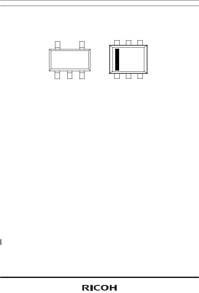
PIN CONFIGURATIONS
SOT-23-5
5 |
4 |
(mark side)
1 2 3
|
SON1612-6 |
|
6 |
5 |
4 |
1 |
2 |
3 |
PIN DESCRIPTIONS
• R1116N (SOT-23-5)
Pin No. |
Symbol |
Description |
|
|
|
1 |
VDD |
Input Pin |
|
|
|
2 |
GND |
Ground Pin |
|
|
|
3 |
CE |
Chip Enable Pin |
|
|
|
4 |
ECO |
MODE alternative pin |
|
|
|
5 |
VOUT |
Output pin |
|
|
|
• R1116D (SON1612-6)
Pin No. |
Symbol |
Description |
|
|
|
1 |
CE |
Chip Enable Pin |
|
|
|
2 |
GND |
Ground Pin |
|
|
|
3 |
VDD |
Input Pin |
|
|
|
4 |
VOUT |
Output Pin |
|
|
|
5 |
GND |
Ground Pin |
|
|
|
6 |
ECO |
MODE alternative pin |
|
|
|
ABSOLUTE MAXIMUM RATINGS
Symbol |
|
|
Item |
Rating |
Unit |
|
|
|
|
|
|
|
|
VIN |
Input Voltage |
6.5 |
V |
|||
|
|
|
|
|
|
|
VECO |
Input Voltage (ECO Pin) |
−0.3 to 6.5 |
V |
|||
|
|
|
|
|
|
|
VCE |
Input Voltage ( |
|
/ CE Pin) |
−0.3 to 6.5 |
V |
|
CE |
||||||
VOUT |
Output Voltage |
−0.3 to VIN+0.3 |
V |
|||
|
|
|
|
|||
IOUT |
Output Current |
180 |
mA |
|||
|
|
|
|
|||
PD |
Power Dissipation (SOT-23-5) 1 |
420 |
mW |
|||
Power Dissipation (SON1612-6) 1 |
500 |
MW |
||||
|
||||||
Topt |
Operating Temperature Range |
−40 ~ 85 |
°C |
|||
Tstg |
Storage Temperature Range |
−55 ~ 125 |
°C |
|||
1 For Power Dissipation, please refer to PACKAGE INFORMATION to be described.
3
R1162x
ELECTRICAL CHARACTERISTICS
• R1162xxx1B/D |
|
|
|
|
|
|
|
|
Topt=25°C |
||
|
|
|
|
|
|
|
|
|
|
||
Symbol |
Item |
|
|
Conditions |
Min. |
Typ. |
Max. |
|
Unit |
||
|
|
VIN = Set VOUT+1V VECO = VIN |
VOUT |
|
VOUT |
|
V |
||||
|
|
< |
< |
|
Note 1 |
×0.98 |
|
×1.02 |
|
||
VOUT |
Output Voltage |
1mA = |
IOUT = 30mA |
|
|
|
|
||||
VIN = Set VOUT + 1V VECO =GND |
VOUT |
|
VOUT |
|
V |
||||||
|
|
|
|
||||||||
|
|
< |
< |
|
Note 2 |
×0.97 |
|
×1.03 |
|
||
|
|
1mA = |
IOUT = 30mA |
|
|
|
|
||||
|
Output Voltage Deviation |
VIN = Set VOUT+1V, IOUT =30mA |
−1.2 |
0.0 |
1.2 |
|
% |
||||
∆VOUT |
between FT Mode and LP |
< |
2.0V |
|
|
|
|||||
VOUT = |
|
|
|
|
|
|
|
||||
|
Mode |
> |
2.0V |
|
|
(−24) |
0.0 |
(24) |
|
mV |
|
|
|
VOUT = |
|
|
|
||||||
IOUT |
Output Current |
VIN − VOUT = 1.0V |
|
|
150 |
|
|
|
mA |
||
|
Load Regulation(FT Mode) |
VIN =Set VOUT+1V, VECO=VIN |
|
20 |
40 |
|
mV |
||||
∆VOUT/ |
< |
|
< |
|
|
|
|
||||
|
1mA = |
IOUT = 150mA |
|
|
|
|
|
|
|||
∆IOUT |
Load Regulation(LP Mode) |
VIN = Set VOUT+1V,VECO=GND |
|
20 |
45 |
|
mV |
||||
|
< |
|
< |
|
|
|
|
||||
|
|
1mA = |
IOUT = 150mA |
|
|
|
|
|
|
||
VDIF |
Dropout Voltage |
Refer to the ELECTRICAL CHARACTERISTICS by OUTPUT VOLTAGE |
|||||||||
ISS1 |
Supply Current(FT Mode) |
VIN = Set VOUT+1V |
|
|
|
70 |
100 |
|
µA |
||
VECO = VIN, IOUT=0mA |
|
|
|
|
|||||||
|
|
|
|
|
|
|
|
|
|||
ISS2 |
Supply Current(LP Mode) |
VIN = Set VOUT+1V |
|
|
|
5.5 |
9.0 |
|
µA |
||
VECO = GND, IOUT=0mA |
|
|
|||||||||
|
|
|
|
|
|
|
|||||
Istandby |
Supply Current (Standby) |
VIN = VCE = Set VOUT+1V |
|
0.1 |
1.0 |
|
µA |
||||
|
|
Set VOUT+0.5V = VIN = 6.0V |
|
|
|
|
|
||||
|
|
|
|
< |
< |
|
|
|
|
|
|
∆VOUT/ |
Line Regulation(FT Mode) |
IOUT = 30mA, VECO = VIN |
|
0.02 |
0.10 |
|
%/V |
||||
|
VOUT = |
1.6V: 2.2V = |
VIN = 6.0V |
|
|
|
|
|
|||
|
|
< |
|
< |
|
< |
|
|
|
|
|
∆VIN |
|
|
|
|
|
|
|
||||
|
Set VOUT + 0.5V = VIN = 6.0V |
|
|
|
|
|
|||||
|
|
|
|
< |
|
< |
|
|
|
|
|
|
Line Regulation(LP Mode) |
IOUT = 30mA, VECO = GND |
|
0.05 |
0.20 |
|
%/V |
||||
|
|
VOUT = |
1.6V: 2.2V = |
VIN = 6.0V |
|
|
|
|
|
||
|
|
< |
|
< |
|
< |
|
|
|
|
|
|
|
f = 1kHz |
|
|
|
|
70 |
|
|
|
|
RR |
Ripple Rejection(FT Mode) |
f = 10kHz,Ripple 0.2Vp-p |
|
60 |
|
|
dB |
||||
|
|
VIN = Set VOUT + 1V |
|
|
|
|
|
|
|
||
|
|
IOUT = 30mA, VECO = VIN |
|
|
|
|
|
||||
VIN |
Input Voltage |
|
|
|
|
|
2.0 |
|
6.0 |
|
V |
∆VOUT/ |
Output Voltage |
IOUT = 30mA |
|
|
|
±100 |
|
|
ppm |
||
∆Topt |
Temperature Coefficient |
−40°C |
< |
< |
|
|
|
|
|
/°C |
|
= |
Topt = 85°C |
|
|
|
|
||||||
Ilim |
Short Current Limit |
VOUT = 0V |
|
|
|
40 |
|
|
mA |
||
IPD |
CE Pull-down |
|
|
|
|
|
|
0.3 |
0.6 |
|
µA |
Constant Current |
|
|
|
|
|
|
|
||||
|
|
|
|
|
|
|
|
|
|
|
|
RPD |
ECO Pull-down Resistance |
|
|
|
|
|
2 |
5 |
30 |
|
MΩ |
VCEH |
CE, ECO Input Voltage “H” |
|
|
|
|
|
1.0 |
|
6.0 |
|
V |
VCEL |
CE, ECO Input Voltage “L” |
|
|
|
|
|
0.00 |
|
0.35 |
|
V |
en |
Output Noise (Fast Mode) |
BW = 10Hz to 100kHz |
|
30 |
|
|
µVrms |
||||
en |
Output Noise |
BW = 10Hz to 100kHz |
|
40 |
|
|
µVrms |
||||
(Low Power Mode) |
|
|
|
||||||||
|
|
|
|
|
|
|
|
|
|
|
|
|
Nch On resistance for |
|
|
|
|
|
|
|
|
|
|
RLOW |
auto-discharge |
VCE=0V |
|
|
|
|
60 |
|
|
Ω |
|
|
(Applied to D version) |
|
|
|
|
|
|
|
|
|
|
4
R1162x
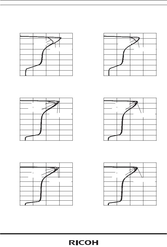
ELECTRICAL CHARACTERISTICS by OUTPUT VOLTAGE
|
|
|
|
|
|
|
Topt = 25°C |
Output Voltage |
|
|
Dropout Voltage (mV) |
|
|
||
|
VDIF(ECO=H) |
|
VDIF(ECO=L) |
||||
VOUT (V) |
Condition |
|
|||||
Typ. |
|
Max. |
|
Typ. |
Max. |
||
|
|
|
|
||||
1.5 =< VOUT =< 1.6 |
|
400 |
|
680 |
|
420 |
680 |
1.6 =< VOUT =< 1.7 |
|
380 |
|
550 |
|
390 |
550 |
1.7 =< VOUT =< 1.8 |
IOUT = 150mA |
350 |
|
520 |
|
370 |
520 |
1.8 =< VOUT =< 2.0 |
340 |
|
490 |
|
350 |
490 |
|
|
|
|
|||||
2.0 =< VOUT =< 2.8 |
|
290 |
|
425 |
|
300 |
430 |
2.8 =< VOUT =< 4.0 |
|
250 |
|
350 |
|
250 |
350 |
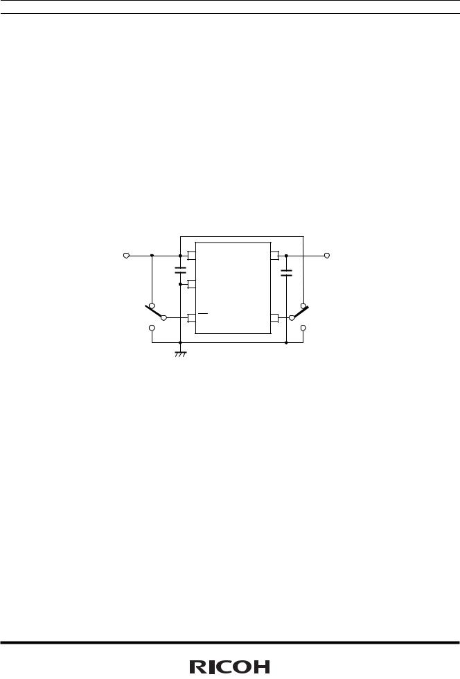
TYPICAL APPLICATION
IN |
VDD |
OUT |
|
|
OUT |
||
C1 |
R1162x |
|
|
SERIES |
C2 |
||
|
|||
|
GND |
||
|
CE CE |
ECO |
(External Components)
C2 Ceramic 0.47µF Ex. Murata GRM40B474K
Kyocera CM105B474K
C1 Ceramic 1.0µF
5
R1162x
TYPICAL CHARACTERISTICS Unless otherwise provided, capacitors are ceramic type.
1) Output Voltage vs. Output Current
R1162x15x (ECO=H)
|
1.6 |
|
|
|
|
OUTH(V) |
1.4 |
|
|
|
|
1.2 |
|
VIN=2V |
|
|
|
|
|
|
|
|
|
V |
1.0 |
|
|
VIN=2.5V • 3.5V |
|
H |
|
|
|||
Voltage |
0.8 |
|
|
|
|
0.6 |
|
|
|
|
|
|
|
|
|
|
|
Output |
0.4 |
|
|
|
|
0.2 |
|
|
|
|
|
|
0.0 |
|
|
|
|
|
0 |
100 |
200 |
300 |
400 |
|
|
Output Current IOUT(mA) |
|
||
R1162x15x (ECO=L)
|
1.6 |
|
|
|
|
OUTL(V) |
1.4 |
|
|
|
|
1.2 |
|
VIN=2V |
|
|
|
|
|
|
|
|
|
L V |
1.0 |
|
|
VIN=2.5V • 3.5V |
|
Voltage |
0.8 |
|
|
|
|
0.6 |
|
|
|
|
|
|
|
|
|
|
|
Output |
0.4 |
|
|
|
|
0.2 |
|
|
|
|
|
|
0.0 |
|
|
|
|
|
0 |
100 |
200 |
300 |
400 |
|
|
Output Current IOUT(mA) |
|
||
R1162x28x (ECO=H)
|
3.0 |
|
|
|
|
OUTH(V) |
2.5 |
VIN=3.1V |
|
|
|
2.0 |
VIN=3.3V |
|
|
|
|
H V |
|
|
VIN=3.8V • 4.8V |
||
|
|
|
|||
Voltage |
1.5 |
|
|
|
|
1.0 |
|
|
|
|
|
Output |
0.5 |
|
|
|
|
|
|
|
|
|
|
|
0.0 |
|
|
|
|
|
0 |
100 |
200 |
300 |
400 |
|
|
Output Current IOUT(mA) |
|
||
R1162x28x (ECO=L)
|
3.0 |
|
|
|
|
OUTL(V) |
2.5 |
VIN=3.1V |
|
|
|
2.0 |
VIN=3.3V |
|
|
|
|
L V |
|
|
VIN=3.8V • 4.8V |
||
|
|
|
|||
Voltage |
1.5 |
|
|
|
|
1.0 |
|
|
|
|
|
Output |
|
|
|
|
|
0.5 |
|
|
|
|
|
|
|
|
|
|
|
|
0.0 |
|
|
|
|
|
0 |
100 |
200 |
300 |
400 |
|
|
Output Current IOUT(mA) |
|
||
R1162x40x (ECO=H)
|
4.5 |
|
|
|
|
OUTH(V) |
4.0 |
VIN=4.3V |
|
|
|
3.5 |
|
|
|||
VIN=4.5V |
|
|
|
||
3.0 |
|
|
|
||
H V |
|
|
VIN=5.0V • 6.0V |
||
2.5 |
|
|
|||
Voltage |
|
|
|
|
|
2.0 |
|
|
|
|
|
1.5 |
|
|
|
|
|
Output |
1.0 |
|
|
|
|
0.5 |
|
|
|
|
|
|
0.0 |
|
|
|
|
|
0 |
100 |
200 |
300 |
400 |
|
|
Output Current IOUT(mA) |
|
||
R1162x40x (ECO=L)
|
4.5 |
|
|
|
|
OUTL(V) |
4.0 |
VIN=4.3V |
|
|
|
3.5 |
|
|
|||
VIN=4.5V |
|
|
|
||
3.0 |
|
|
|
||
L V |
|
|
VIN=5.0V • 6.0V |
||
2.5 |
|
|
|||
Voltage |
|
|
|
|
|
2.0 |
|
|
|
|
|
1.5 |
|
|
|
|
|
Output |
|
|
|
|
|
1.0 |
|
|
|
|
|
0.5 |
|
|
|
|
|
|
0.0 |
|
|
|
|
|
0 |
100 |
200 |
300 |
400 |
|
|
Output Current IOUT(mA) |
|
||
6
R1162x
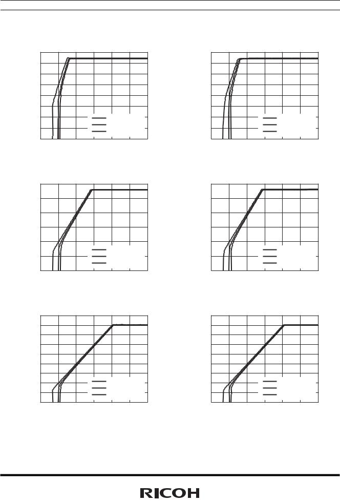
2) Output Voltage vs. Input Voltage
R1162x15x (ECO=H)
H(V)OUT |
1.6 |
|
|
|
|
|
|
1.4 |
|
|
|
|
|
|
|
|
|
|
|
|
|
|
|
|
1.2 |
|
|
|
|
|
|
V |
1.0 |
|
|
|
|
|
|
H |
|
|
|
|
|
|
|
|
|
|
|
|
|
|
|
Voltage |
0.8 |
|
|
|
|
|
|
|
|
|
|
|
|
|
|
|
0.6 |
|
|
|
|
|
|
Output |
0.4 |
|
|
|
IOUT=1mA |
|
|
0.2 |
|
|
|
IOUT=30mA |
|
||
|
0.0 |
|
|
|
IOUT=50mA |
|
|
|
|
|
|
|
|
|
|
|
0 |
1 |
2 |
3 |
4 |
5 |
6 |
|
|
|
Input Voltage VIN(V) |
|
|
||
R1162x28x (ECO=H)
|
3.0 |
|
|
|
|
|
|
VOUTH(V) |
2.5 |
|
|
|
|
|
|
2.0 |
|
|
|
|
|
|
|
H |
|
|
|
|
|
|
|
Voltage |
1.5 |
|
|
|
|
|
|
1.0 |
|
|
|
|
|
|
|
Output |
0.5 |
|
|
|
IOUT=1mA |
|
|
|
|
|
IOUT=30mA |
|
|||
|
|
|
|
IOUT=50mA |
|
||
|
0.0 |
|
|
|
|
||
|
|
|
|
|
|
|
|
|
0 |
1 |
2 |
3 |
4 |
5 |
6 |
|
|
|
Input Voltage VIN(V) |
|
|
||
R1162x40x (ECO=H)
|
4.5 |
|
|
|
|
|
|
VOUTH(V) |
4.0 |
|
|
|
|
|
|
3.5 |
|
|
|
|
|
|
|
3.0 |
|
|
|
|
|
|
|
H |
2.5 |
|
|
|
|
|
|
Voltage |
|
|
|
|
|
|
|
2.0 |
|
|
|
|
|
|
|
1.5 |
|
|
|
|
|
|
|
Output |
1.0 |
|
|
|
IOUT=1mA |
|
|
0.5 |
|
|
|
IOUT=30mA |
|
||
|
|
|
IOUT=50mA |
|
|||
|
0.0 |
|
|
|
|
||
|
|
|
|
|
|
|
|
|
0 |
1 |
2 |
3 |
4 |
5 |
6 |
|
|
|
Input Voltage VIN(V) |
|
|
||
R1162x15x (ECO=L)
|
1.6 |
|
|
|
|
|
|
OUTL(V) |
1.4 |
|
|
|
|
|
|
1.2 |
|
|
|
|
|
|
|
|
|
|
|
|
|
|
|
L V |
1.0 |
|
|
|
|
|
|
Voltage |
0.8 |
|
|
|
|
|
|
0.6 |
|
|
|
|
|
|
|
|
|
|
|
|
|
|
|
Output |
0.4 |
|
|
|
IOUT=1mA |
|
|
0.2 |
|
|
|
IOUT=30mA |
|
||
|
0.0 |
|
|
|
IOUT=50mA |
|
|
|
|
|
|
|
|
|
|
|
0 |
1 |
2 |
3 |
4 |
5 |
6 |
|
|
|
Input Voltage VIN(V) |
|
|
||
R1162x28x (ECO=L)
|
3.0 |
|
|
|
|
|
|
VOUTL(V) |
2.5 |
|
|
|
|
|
|
2.0 |
|
|
|
|
|
|
|
L |
|
|
|
|
|
|
|
Voltage |
1.5 |
|
|
|
|
|
|
1.0 |
|
|
|
|
|
|
|
Output |
|
|
|
IOUT=1mA |
|
||
0.5 |
|
|
|
|
|||
|
|
|
IOUT=30mA |
|
|||
|
|
|
|
IOUT=50mA |
|
||
|
0.0 |
|
|
|
|
||
|
|
|
|
|
|
|
|
|
0 |
1 |
2 |
3 |
4 |
5 |
6 |
|
|
|
Input Voltage VIN(V) |
|
|
||
|
|
R1162x40x (ECO=L) |
|
|
|||
|
4.5 |
|
|
|
|
|
|
VOUTL(V) |
4.0 |
|
|
|
|
|
|
3.0 |
|
|
|
|
|
|
|
|
3.5 |
|
|
|
|
|
|
L |
2.5 |
|
|
|
|
|
|
Voltage |
|
|
|
|
|
|
|
2.0 |
|
|
|
|
|
|
|
|
|
|
|
|
|
|
|
Output |
1.5 |
|
|
|
IOUT=1mA |
|
|
0.5 |
|
|
|
|
|||
|
1.0 |
|
|
|
|
||
|
|
|
|
|
IOUT=30mA |
|
|
|
0.0 |
|
|
|
IOUT=50mA |
|
|
|
|
|
|
|
|
|
|
|
0 |
1 |
2 |
3 |
4 |
5 |
6 |
|
|
|
Input Voltage VIN(V) |
|
|
||
7

R1162x
3) Supply Current vs. Input Voltage
R1162x15x (ECO=H)
|
80 |
|
|
|
|
|
|
A) |
70 |
|
|
|
|
|
|
H( |
60 |
|
|
|
|
|
|
H ISS |
50 |
|
|
|
|
|
|
Current |
40 |
|
|
|
|
|
|
30 |
|
|
|
|
|
|
|
|
|
|
|
|
|
|
|
Supply |
20 |
|
|
|
|
|
|
10 |
|
|
|
|
|
|
|
|
0 |
|
|
|
|
|
|
|
0 |
1 |
2 |
3 |
4 |
5 |
6 |
|
|
|
Input Voltage VIN(V) |
|
|
||
R1162x28x (ECO=H)
|
80 |
|
|
|
|
|
|
A) |
70 |
|
|
|
|
|
|
|
60 |
|
|
|
|
|
|
SSH( |
|
|
|
|
|
|
|
|
|
|
|
|
|
|
|
H I |
50 |
|
|
|
|
|
|
Current |
40 |
|
|
|
|
|
|
30 |
|
|
|
|
|
|
|
|
|
|
|
|
|
|
|
Supply |
20 |
|
|
|
|
|
|
10 |
|
|
|
|
|
|
|
|
0 |
|
|
|
|
|
|
|
0 |
1 |
2 |
3 |
4 |
5 |
6 |
|
|
|
Input Voltage VIN(V) |
|
|
||
R1162x40x (ECO=H)
|
80 |
|
|
|
|
|
|
A) |
70 |
|
|
|
|
|
|
|
60 |
|
|
|
|
|
|
SSH( |
|
|
|
|
|
|
|
|
|
|
|
|
|
|
|
H I |
50 |
|
|
|
|
|
|
Current |
40 |
|
|
|
|
|
|
30 |
|
|
|
|
|
|
|
|
|
|
|
|
|
|
|
Supply |
20 |
|
|
|
|
|
|
10 |
|
|
|
|
|
|
|
|
0 |
|
|
|
|
|
|
|
0 |
1 |
2 |
3 |
4 |
5 |
6 |
|
|
|
Input Voltage VIN(V) |
|
|
||
R1162x15x (ECO=L)
|
7 |
|
|
|
|
|
|
A) |
6 |
|
|
|
|
|
|
SSL( |
5 |
|
|
|
|
|
|
L I |
4 |
|
|
|
|
|
|
Current |
|
|
|
|
|
|
|
3 |
|
|
|
|
|
|
|
2 |
|
|
|
|
|
|
|
Supply |
|
|
|
|
|
|
|
1 |
|
|
|
|
|
|
|
|
0 |
|
|
|
|
|
|
|
0 |
1 |
2 |
3 |
4 |
5 |
6 |
|
|
|
Input Voltage VIN(V) |
|
|
||
R1162x28x (ECO=L)
|
11 |
|
|
|
|
|
|
A) |
10 |
|
|
|
|
|
|
9 |
|
|
|
|
|
|
|
SSL( |
8 |
|
|
|
|
|
|
|
|
|
|
|
|
|
|
L I |
7 |
|
|
|
|
|
|
Current |
6 |
|
|
|
|
|
|
5 |
|
|
|
|
|
|
|
4 |
|
|
|
|
|
|
|
Supply |
3 |
|
|
|
|
|
|
2 |
|
|
|
|
|
|
|
1 |
|
|
|
|
|
|
|
|
|
|
|
|
|
|
|
|
0 |
|
|
|
|
|
|
|
0 |
1 |
2 |
3 |
4 |
5 |
6 |
|
|
|
Input Voltage VIN(V) |
|
|
||
R1162x40x (ECO=L)
|
12 |
|
A) |
11 |
|
10 |
||
ISSL( |
9 |
|
8 |
||
L |
7 |
|
Current |
6 |
|
|
||
|
5 |
|
Supply |
4 |
|
3 |
||
|
2
1
0
0 |
1 |
2 |
3 |
4 |
5 |
6 |
|
|
Input Voltage VIN(V) |
|
|
||
8
R1162x
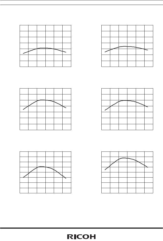
4) Output Voltage vs. Temperature
R1162x15x (ECO=H)
|
1.53 |
|
|
|
|
|
|
(V) |
1.52 |
|
|
|
|
|
|
VOUTH |
1.51 |
|
|
|
|
|
|
|
|
|
|
|
|
|
|
H |
1.50 |
|
|
|
|
|
|
Voltage |
|
|
|
|
|
|
|
1.49 |
|
|
|
|
|
|
|
1.48 |
|
|
|
|
|
|
|
Output |
|
|
|
|
|
|
|
1.47 |
|
|
|
|
|
|
|
|
|
|
|
|
|
|
|
|
1.46 |
|
|
|
|
|
|
|
-50 |
-25 |
0 |
25 |
50 |
75 |
100 |
|
|
|
Temperature Topt(°C) |
|
|
||
R1162x28x (ECO=H)
|
2.83 |
|
|
|
|
|
|
(V) |
2.82 |
|
|
|
|
|
|
VOUTH |
2.81 |
|
|
|
|
|
|
|
|
|
|
|
|
|
|
H |
2.80 |
|
|
|
|
|
|
Voltage |
|
|
|
|
|
|
|
2.79 |
|
|
|
|
|
|
|
2.78 |
|
|
|
|
|
|
|
Output |
|
|
|
|
|
|
|
2.77 |
|
|
|
|
|
|
|
|
|
|
|
|
|
|
|
|
2.76 |
|
|
|
|
|
|
|
-50 |
-25 |
0 |
25 |
50 |
75 |
100 |
|
|
|
Temperature Topt(°C) |
|
|
||
R1162x40x (ECO=H)
|
4.05 |
|
|
|
|
|
|
(V) |
4.04 |
|
|
|
|
|
|
VOUTH |
4.03 |
|
|
|
|
|
|
4.02 |
|
|
|
|
|
|
|
H |
|
|
|
|
|
|
|
|
|
|
|
|
|
|
|
Voltage |
4.01 |
|
|
|
|
|
|
4.00 |
|
|
|
|
|
|
|
|
|
|
|
|
|
|
|
Output |
3.99 |
|
|
|
|
|
|
3.98 |
|
|
|
|
|
|
|
|
3.97 |
|
|
|
|
|
|
|
-50 |
-25 |
0 |
25 |
50 |
75 |
100 |
|
|
|
Temperature Topt(°C) |
|
|
||
R1162x15x (ECO=L)
|
1.53 |
|
|
|
|
|
|
(V) |
1.52 |
|
|
|
|
|
|
VOUTL |
1.51 |
|
|
|
|
|
|
|
|
|
|
|
|
|
|
L |
1.50 |
|
|
|
|
|
|
Voltage |
|
|
|
|
|
|
|
1.49 |
|
|
|
|
|
|
|
1.48 |
|
|
|
|
|
|
|
Output |
|
|
|
|
|
|
|
1.47 |
|
|
|
|
|
|
|
|
|
|
|
|
|
|
|
|
1.46 |
|
|
|
|
|
|
|
-50 |
-25 |
0 |
25 |
50 |
75 |
100 |
|
|
|
Temperature Topt(°C) |
|
|
||
R1162x28x (ECO=L)
|
2.83 |
|
|
|
|
|
|
(V) |
2.82 |
|
|
|
|
|
|
VOUTL |
2.81 |
|
|
|
|
|
|
|
|
|
|
|
|
|
|
L |
2.80 |
|
|
|
|
|
|
Voltage |
|
|
|
|
|
|
|
2.79 |
|
|
|
|
|
|
|
2.78 |
|
|
|
|
|
|
|
Output |
|
|
|
|
|
|
|
2.77 |
|
|
|
|
|
|
|
|
|
|
|
|
|
|
|
|
2.76 |
|
|
|
|
|
|
|
-50 |
-25 |
0 |
25 |
50 |
75 |
100 |
|
|
|
Temperature Topt(°C) |
|
|
||
R1162x40x (ECO=L)
|
4.06 |
|
|
|
|
|
|
(V) |
4.05 |
|
|
|
|
|
|
|
|
|
|
|
|
|
|
VOUTL |
4.04 |
|
|
|
|
|
|
4.03 |
|
|
|
|
|
|
|
L |
|
|
|
|
|
|
|
Voltage |
4.02 |
|
|
|
|
|
|
4.01 |
|
|
|
|
|
|
|
|
|
|
|
|
|
|
|
Output |
4.00 |
|
|
|
|
|
|
3.99 |
|
|
|
|
|
|
|
|
3.98 |
|
|
|
|
|
|
|
-50 |
-25 |
0 |
25 |
50 |
75 |
100 |
|
|
|
Temperature Topt(°C) |
|
|
||
9

R1162x
5) Supply Current vs. Temperature
R1162x15x (ECO=H)
|
90 |
|
|
|
|
|
|
A) |
80 |
|
|
|
|
|
|
H( |
70 |
|
|
|
|
|
|
ISS |
60 |
|
|
|
|
|
|
H |
50 |
|
|
|
|
|
|
Current |
|
|
|
|
|
|
|
40 |
|
|
|
|
|
|
|
30 |
|
|
|
|
|
|
|
Supply |
|
|
|
|
|
|
|
20 |
|
|
|
|
|
|
|
10 |
|
|
|
|
|
|
|
|
0 |
|
|
|
|
|
|
|
-50 |
-25 |
0 |
25 |
50 |
75 |
100 |
|
|
|
Temperature Topt(°C) |
|
|
||
R1162x28x (ECO=H)
|
90 |
|
|
|
|
|
|
A) |
80 |
|
|
|
|
|
|
|
70 |
|
|
|
|
|
|
ISSH( |
|
|
|
|
|
|
|
60 |
|
|
|
|
|
|
|
H |
50 |
|
|
|
|
|
|
Current |
|
|
|
|
|
|
|
40 |
|
|
|
|
|
|
|
30 |
|
|
|
|
|
|
|
Supply |
|
|
|
|
|
|
|
20 |
|
|
|
|
|
|
|
10 |
|
|
|
|
|
|
|
|
0 |
|
|
|
|
|
|
|
-50 |
-25 |
0 |
25 |
50 |
75 |
100 |
|
|
|
Temperature Topt(°C) |
|
|
||
R1162x40x (ECO=H)
|
90 |
|
|
|
|
|
|
A) |
80 |
|
|
|
|
|
|
|
70 |
|
|
|
|
|
|
ISSH( |
|
|
|
|
|
|
|
60 |
|
|
|
|
|
|
|
H |
50 |
|
|
|
|
|
|
Current |
|
|
|
|
|
|
|
40 |
|
|
|
|
|
|
|
30 |
|
|
|
|
|
|
|
Supply |
|
|
|
|
|
|
|
20 |
|
|
|
|
|
|
|
10 |
|
|
|
|
|
|
|
|
0 |
|
|
|
|
|
|
|
-50 |
-25 |
0 |
25 |
50 |
75 |
100 |
|
|
|
Temperature Topt(°C) |
|
|
||
R1162x15x (ECO=L)
|
8 |
|
|
|
|
|
|
A) |
7 |
|
|
|
|
|
|
L( |
6 |
|
|
|
|
|
|
L ISS |
5 |
|
|
|
|
|
|
Current |
4 |
|
|
|
|
|
|
3 |
|
|
|
|
|
|
|
Supply |
2 |
|
|
|
|
|
|
1 |
|
|
|
|
|
|
|
|
0 |
|
|
|
|
|
|
|
-50 |
-25 |
0 |
25 |
50 |
75 |
100 |
|
|
|
Temperature Topt(°C) |
|
|
||
R1162x28x (ECO=L)
|
8 |
|
|
|
|
|
|
A) |
7 |
|
|
|
|
|
|
|
6 |
|
|
|
|
|
|
L ISSL( |
|
|
|
|
|
|
|
5 |
|
|
|
|
|
|
|
Current |
4 |
|
|
|
|
|
|
3 |
|
|
|
|
|
|
|
Supply |
2 |
|
|
|
|
|
|
1 |
|
|
|
|
|
|
|
|
0 |
|
|
|
|
|
|
|
-50 |
-25 |
0 |
25 |
50 |
75 |
100 |
|
|
|
Temperature Topt(°C) |
|
|
||
R1162x40x (ECO=L)
|
8 |
|
|
|
|
|
|
A) |
7 |
|
|
|
|
|
|
|
6 |
|
|
|
|
|
|
L ISSL( |
|
|
|
|
|
|
|
5 |
|
|
|
|
|
|
|
Current |
4 |
|
|
|
|
|
|
3 |
|
|
|
|
|
|
|
Supply |
2 |
|
|
|
|
|
|
1 |
|
|
|
|
|
|
|
|
0 |
|
|
|
|
|
|
|
-50 |
-25 |
0 |
25 |
50 |
75 |
100 |
|
|
|
Temperature Topt(°C) |
|
|
||
10
 Loading...