


Richtek RT9818A-13PY, RT9818A-14PV, RT9818A-15PV, RT9818A-16PV, RT9818A-18GV Schematic [ru]
...RT9818
Features
zInternally Fixed Threshold 1.2V to 5V in 0.1V Step
zHigh Accuracy ±1.5%
zLow Supply Current 3μA
zNo External Components Required
zQuick Reset within 20μs
zBuilt-in Recovery Delay Include 0ms, 55ms, 220ms, 450ms Options
zLow Functional Supply Voltage 0.9V
zN-Channel Open-Drain Output
zSmall SC-82, SC-70-3, SOT-23-3, SOT-23-5, SOT-89 Packages
zRoHS Compliant and 100% Lead (Pb)-Free
Applications
zComputers
zControllers
zIntelligent Instruments
zCritical μP and μC Power Monitoring
zPortable/Battery-Powered Equipment
Marking Information
For marking information, contact our sales representative directly or through a Richtek distributor located in your area.
Typical Application Circuit
|
|
|
|
|
|
|
|
|
|
|
|
|
|
|
|
|
|
|
|
|
|
|
|
|
|
|
|
|
|
|
|
|
|
|
|
100k |
|
RT9818 |
|
||||||||
|
|
|
|
|
|
|
|
|
|
|
|
Pull Up |
|
|
GND |
|
|||||||
|
VDD |
|
|
|
|
|
|
|
|
|
|
|
|
VDD |
|
||||||||
|
|
μP |
|
|
|
|
|
|
|
|
|
|
|
|
|
|
|||||||
|
|
|
|
|
|
|
|
|
|
|
|
|
|
|
|
||||||||
|
|
|
|
|
|
|
|
|
|
|
|
|
|
|
|
|
|
|
|
|
|
|
|
|
|
|
|
|
|
|
|
|
|
|
|
|
|
|
|
|
|
|
|
|
RESET/ |
|
|
RESET/ |
|
|
|
|
|
|
|
|
|
|
|
|
|
||||||||||
|
|
|
|
|
|
|
|
|
|
|
RESET |
|
|||||||||||
|
RESET |
|
|
|
|
|
|
|
|
|
|
|
|
||||||||||
|
|
|
|
|
|
|
|
|
|
|
|
|
|
|
|||||||||
|
|
|
|
||||||||||||||||||||
|
|
|
|
|
|
|
|
|
|
|
|
|
|
|
|
|
|
|
|
|
|
|
|
|
|
|
|
|
|
|
|
|
|
|
|
|
|
|
|
|
|
|
|
|
|
|
|
|
|
|
|
|
|
|
|
|
|
|
|
|
|
|
|
|
|
|
|
|
|
|
|
|
|
|
|
|
|
|
|
|
|
|
|
|
|
|
|
|
|
|
|
|
|
|
|
is a registered trademark of Richtek Technology Corporation.
www.richtek.com
1
RT9818
Pin Configurations
(TOP VIEW)
|
|
GND |
|
NC |
|
|
|
|
|
|
|
|
|
|
|
|
VDD |
||||||||||||
|
|
|
RESET/ |
|
NC |
|
|
||||||||||||||||||||||
|
|
|
|
|
|
|
|
|
|
|
|
|
|
||||||||||||||||
|
|
|
|
|
|
|
|
|
|
|
RESET |
|
|
|
|
|
|
|
|
|
|
|
|||||||
|
|
|
|
|
|
|
|
|
|
|
|
|
|
|
|
|
|
|
|
||||||||||
|
|
|
4 |
|
|
|
|
3 |
|
|
|
|
|
|
|
|
|
|
|
3 |
|
|
|
|
|
|
|||
|
|
|
|
|
|
|
|
|
|
|
|
|
|
|
|
|
|
|
|
|
|
|
|
|
|
|
|
|
|
|
|
|
|
|
|
|
|
|
|
|
|
|
4 |
|
|
|
3 |
|
|
|
|
|
|
|
|
|
|
|
|
|
|
|
|
|
|
|
2 |
|
|
|
|
|
|
|
|
|
|
|
2 |
|
|
|
|||||||
|
|
|
|
|
|
|
|
|
|
|
|
|
|
|
|
2 |
|
|
|
|
|
|
|
|
|
|
|
|
|
|
|
|
|
|
|
VDD |
|
|
|
|
|
|
|
|
|
|
|
|
|
|
|
|
|
|
|
|
|||
|
RESET/ |
|
|
|
|
|
|
|
|
|
|
|
GND |
RESET/ |
|
||||||||||||||
|
|
VDD |
GND |
|
|||||||||||||||||||||||||
|
RESET |
|
|
|
|
|
|
|
|
|
|
|
RESET |
||||||||||||||||
|
|
|
|
|
|
|
|
|
|
|
|
|
|
|
|
|
|
|
|
|
|
|
|
|
|||||
|
|
|
SC-82 |
SC-82 (R-Type) |
|
SC-70-3 |
|||||||||||||||||||||||
VDD |
VDD |
NC |
NC |
|||||||||||
|
|
|
|
|
|
|
|
|
|
|
|
|
|
|
|
|
|
|
|
|
|
|
|
|
|
|
|
|
|
3 |
|
|
3 |
|
|
5 |
|
|
4 |
|
||||
2 |
|
2 |
|
2 |
3 |
|
||||||||
|
|
|
|
|
|
|
|
|
|
|
|
|
|
|
1 |
2 |
3 |
|
|
|
|
|
|
|
|
|
|
|
|
|
|
|
VDD GND |
|
|
|
|
|
|
|
|
|
|
|
|
|
|
GND |
|
GND |
|
|
|
|
RESET/ |
|
|
|
|
|
|
|
|
|
|||
RESET/ |
|
|
RESET/ |
|
|
|
|
VDD GND |
||||||||||||||||
|
|
RESET/ |
||||||||||||||||||||||
|
|
|
|
|
|
RESET |
||||||||||||||||||
RESET |
|
|
|
|
|
|
RESET |
RESET |
|
|
|
|
|
|||||||||||
|
SOT-23-3 |
SOT-23-3 (L-Type) |
SOT-23-5 |
SOT-89 |
||||||||||||||||||||
|
|
|
|
|
||||||||||||||||||||
Functional Pin Description
|
Pin Name |
Pin Function |
|
GND |
Ground |
||
|
Active Low Open-Drain Reset Output |
||
|
RESET |
|
|
RESET |
Active High Open-Drain Reset Output |
||
VDD |
Power Pin |
||
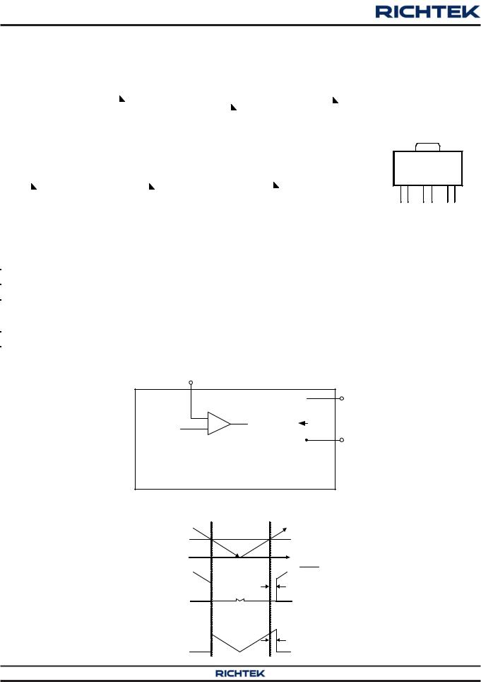
Function Block Diagram
|
|
|
VDD |
|
|
|
|
|
|
|
|
|
|
|
|
|
|
|
|
|||
|
|
|
|
|
|
|
|
|
|
|
|
|
|
|
|
|
|
|
|
|
|
|
|
|
|
|
|
|
|
|
|
|
|
|
|
|
|
|
|
|
|
|
|
RESET/ |
|
|
|
|
|
|
|
|
|
|
|
|
|
|
|
|
|
|
|
|
|
|
RESET |
|
|
|
|
|
|
|
|
|
|
|
|
|
|
|
|
|
|
|
|
|
|
|
|
|
|
|
|
CMP |
|
Timer |
|
|
|
|
|
|
|
|
|
N MOS |
||||||
|
VSET |
|
|
|
|
|
|
|
|
|
|
|
|
|
|
|
|
|
|
|
GND |
|
|
|
|
|
|
|
|
|
|
|
|
|
|
|
|
|
|
|
|
|
|
||
|
Threshold |
|
|
|
|
|
|
|||||||||||||||
|
|
|
|
|
|
|
|
|
|
|
|
|
|
|
|
|
|
|
|
|
||
Voltage Setting |
|
|
|
|
|
|
|
|
|
|
|
|
|
|
|
|
|
|
||||
POR |
|
|
|
|
|
|
|
|
|
|
|
|
|
|
|
|
|
|
||||
|
|
|
|
|
|
|
|
|
|
|
|
|
|
|
|
|
|
|
|
|
||
|
|
|
|
|
|
|
|
|
|
|
|
|
|
|
|
|
|
|
|
|
|
|
|
|
|
|
|
|
|
|
|
|
|
|
|
|
|
|
|
|
|
|
|
|
|
|
|
|
Power On Reset |
|
|
|
|
|
|
|
|
|
|
|
|
|
|
|
|
|||
Timing Diagram
|
VDD |
|
VTH |
|
0V |
|
VRESET |
|
Delay Time (0, 55, 220, 450ms) |
|
0V |
|
VRESET |
|
Delay Time (0, 55, 220, 450ms) |
|
0V |
Copyright ©2013 Richtek Technology Corporation. All rights reserved. |
is a registered trademark of Richtek Technology Corporation. |
www.richtek.com |
DS9818-10 May 2013 |
2 |
|
|
RT9818 |
Absolute Maximum Ratings (Note 1) |
|
z Terminal Voltage (with Respect to GND) |
|
VDD --------------------------------------------------------------------------------------------------------------------- |
−0.3V to 6V |
z All Other Inputs ----------------------------------------------------------------------------------------------------- |
−0.3V to (VDD + 0.3V) |
z Input Current, IVDD -------------------------------------------------------------------------------------------------- |
20mA |
z Power Dissipation, PD @ TA = 25°C |
|
SC-70 / SC-82------------------------------------------------------------------------------------------------------- |
0.25W |
SOT-23-3 ------------------------------------------------------------------------------------------------------------- |
0.4W |
SOT-23-5 ------------------------------------------------------------------------------------------------------------- |
0.4W |
SOT-89 ---------------------------------------------------------------------------------------------------------------- |
0.55W |
z Package Thermal Resistance (Note 2) |
|
SC-70 / SC-82, θJA ------------------------------------------------------------------------------------------------- |
400°C/W |
SOT-23-3, θJA -------------------------------------------------------------------------------------------------------- |
250°C/W |
SOT-23-5, θJA -------------------------------------------------------------------------------------------------------- |
250°C/W |
SOT-89, θJA ---------------------------------------------------------------------------------------------------------- |
180°C/W |
z Lead Temperature (Soldering, 10sec.)------------------------------------------------------------------------- |
260°C |
z Storage Temperature Range ------------------------------------------------------------------------------------- |
−65°C to 150°C |
z ESD Susceptibility (Note 3) |
|
HBM (Human Body Model) --------------------------------------------------------------------------------------- |
2kV |
Recommended Operating Conditions |
(Note 4) |
z Junction Temperature Range ------------------------------------------------------------------------------------- |
−40°C to 125°C |
z Ambient Temperature Range ------------------------------------------------------------------------------------- |
−40°C to 85°C |
Electrical Characteristics
(VDD = 3V, unless otherwise specified)
Parameter |
Symbol |
Test Conditions |
Min |
Typ |
Max |
Unit |
|
Operating VDD (VOUT) Range |
VDD |
|
0.9 |
-- |
6 |
V |
|
Supply Current |
|
IDD |
VTH = 3V, VDD = 4.5V, TA = 27°C |
-- |
3 |
8 |
μA |
Reset Threshold |
|
VTH |
TA = 27°C |
-- |
1.2 to 5 |
-- |
V |
Threshold Voltage Accuracy |
VTH |
TA = 27°C |
−1.5 |
-- |
1.5 |
% |
|
VDD Drop to Reset Delay |
tRD |
Drop = VTH −125mV |
-- |
20 |
-- |
μs |
|
|
RT9818A/E |
|
|
-- |
0 |
-- |
|
Reset Active |
RT9818B/F |
tRP |
VDD ≥ 1.02 x VTH |
35 |
55 |
75 |
ms |
Time Out Period |
RT9818C/G |
143 |
220 |
297 |
|||
|
RT9818D/H |
|
|
292 |
450 |
608 |
|
RESET Output Voltage Low |
VOL |
3 = VDD < VTH ISINK > 3.5mA |
-- |
-- |
0.4 |
V |
|
(Note 5) |
|
||||||
|
|
|
|
|
|
|
|
Hysteresis Width |
|
VHYS |
|
-- |
0.01VTH |
0.016VTH |
V |
Copyright ©2013 Richtek Technology Corporation. All rights reserved. |
is a registered trademark of Richtek Technology Corporation. |
DS9818-10 May 2013 |
www.richtek.com |
|
3 |

RT9818
Note 1. Stresses beyond those listed “Absolute Maximum Ratings” may cause permanent damage to the device. These are stress ratings only, and functional operation of the device at these or any other conditions beyond those indicated in the operational sections of the specifications is not implied. Exposure to absolute maximum rating conditions may affect device reliability.
Note 2. θJA is measured at TA = 25°C on a low effective thermal conductivity single-layer test board per JEDEC 51-3. Note 3. Devices are ESD sensitive. Handling precaution is recommended.
Note 4. The device is not guaranteed to function outside its operating conditions.
Note 5. The voltage VOL can be calculated by VOL = VDD − Ir * R. Where R is the pull-up resistor and Ir is the current flowing through the pull-up resistor. For typical application (R=100kΩ), VOL is less than 0.2V.
Copyright ©2013 Richtek Technology Corporation. All rights reserved. |
is a registered trademark of Richtek Technology Corporation. |
www.richtek.com |
DS9818-10 May 2013 |
4 |
|

RT9818
Typical Operating Characteristics
Nch Driver Output Current vs. VDS
|
2.4 |
RT9818A-12 |
|
|
|
|
|
|
|
|
|
|
|
(mA) |
2.0 |
|
|
|
VDD = 1.1V |
|
|
|
|
|
|
||
|
|
|
|
|
|
|
Current |
1.6 |
|
|
|
|
|
1.2 |
|
|
|
|
|
|
Output |
|
|
|
|
|
|
0.8 |
|
|
|
VDD = 1V |
|
|
|
|
|
|
|
||
|
|
|
|
|
|
|
|
0.4 |
|
|
|
|
|
|
0.0 |
|
|
|
|
|
|
0 |
0.3 |
0.6 |
0.9 |
1.2 |
1.5 |
VDS (V)
|
120 |
Nch Driver Output Current vs. VDS |
|
|||
|
RT9818A-45 |
|
|
|
|
|
|
|
|
|
|
|
|
|
100 |
|
|
|
|
|
(mA) |
80 |
|
|
|
|
|
Current |
60 |
|
|
|
VDD = 4.4V |
|
|
|
|
|
|
||
|
|
|
|
|
|
|
Output |
|
|
|
|
= 4V |
|
40 |
|
|
|
= 3.5V |
|
|
|
|
|
|
|
= 3V |
|
|
20 |
|
|
|
= 2.5V |
|
|
|
|
|
= 2V |
|
|
|
|
|
|
|
|
|
|
|
|
|
|
= 1.5V |
|
|
0 |
|
|
|
|
|
|
0 |
1 |
2 |
3 |
4 |
5 |
VDS (V)
Supply Current vs. Input Voltage
|
6 |
RT9818A-12 |
|
|
|
|
|
(μA) |
5 |
|
|
|
80°C |
|
|
4 |
|
|
|
|
|
|
|
Current |
|
|
|
|
|
|
|
|
|
|
|
25°C |
|
|
|
3 |
|
|
|
|
|
|
|
|
|
|
|
|
|
|
|
Supply |
2 |
|
|
|
−30°C |
|
|
|
|
|
|
|
|
||
|
|
|
|
|
|
|
|
|
1 |
|
|
|
|
|
|
|
0 |
|
|
|
|
|
|
|
0 |
1 |
2 |
3 |
4 |
5 |
6 |
Input Voltage (V)
Nch Driver Output Current vs. VDS
|
60 |
RT9818C-30 |
|
|
|
|
|
|
|
|
|
|
|
|
|
|
|
|
50 |
|
|
|
|
|
VDD = 2.8V |
|
|
|
|
|
|
|
|
|
|
(mA) |
40 |
|
|
|
|
VDD = 2.5V |
|
|
Current |
30 |
|
|
|
|
VDD = 2V |
|
|
|
|
|
|
|
|
|
||
Output |
20 |
|
|
|
|
|
|
|
|
|
|
VDD = 1.5V |
|
|
|||
|
10 |
|
|
|
|
|||
|
|
|
|
|
|
|
|
|
|
0 |
|
|
|
|
|
|
|
|
0 |
0.5 |
1 |
1.5 |
2 |
2.5 |
3 |
3.5 |
VDS (V)
Output Voltage vs. Input Voltage
|
7 |
RT9818 |
|
|
|
|
|
|
|
|
|
|
|
|
|
|
6 |
|
|
|
|
|
|
(V) |
5 |
|
|
|
|
|
|
Voltage |
4 |
|
|
|
|
|
|
3 |
|
|
|
|
|
|
|
Output |
|
|
|
|
|
|
|
2 |
|
|
|
|
4.5V |
|
|
|
|
|
|
|
|
||
|
1 |
|
1.2V |
|
|
|
|
|
|
|
|
|
|
|
|
|
0 |
|
|
|
|
|
|
|
0 |
1 |
2 |
3 |
4 |
5 |
6 |
Input Voltage (V)
Supply Current vs. Input Voltage
|
4.0 |
RT9818C-30 |
|
|
|
|
|
|
|
|
|
|
|
|
|
|
3.5 |
|
|
|
|
|
|
A) |
3.0 |
|
|
|
80°C |
|
|
(μ |
|
|
|
|
|
|
|
Current |
2.5 |
|
|
|
25°C |
|
|
2.0 |
|
|
|
|
|
||
|
|
|
|
|
|
||
|
|
|
|
|
|
|
|
Supply |
1.5 |
|
|
|
−30°C |
|
|
|
|
|
|
|
|
||
1.0 |
|
|
|
|
|
|
|
|
0.5 |
|
|
|
|
|
|
|
0.0 |
|
|
|
|
|
|
|
0 |
1 |
2 |
3 |
4 |
5 |
6 |
Input Voltage (V)
Copyright ©2013 Richtek Technology Corporation. All rights reserved. |
is a registered trademark of Richtek Technology Corporation. |
DS9818-10 May 2013 |
www.richtek.com |
|
5 |
 Loading...