


Richtek RT9715AGB, RT9715AGF, RT9715AGQW, RT9715BGB, RT9715BGBG Schematic [ru]
...RT9715
90mΩ, 2A/1.5A/1.1A/0.7A High-Side Power Switches with Flag
General Description |
Features |
The RT9715 is a cost-effective, low-voltage, single N-MOSFET high-side Power Switch IC for USB application. Low switch-on resistance (typ. 90mΩ) and low supply current (typ. 50uA) are realized in this IC.
The RT9715 integrates an over-current protection circuit, a short fold back circuit, a thermal shutdown circuit and an under-voltage lockout circuit for overall protection. Besides, a flag output is available to indicate fault conditions to the local USB controller. Furthermore, the chip also integrates an embedded delay function to prevent miss-operation from happening due to inrush-current. The RT9715 is an ideal solution for USB power supply and can support flexible applications since it is available in various packages such as SOT-23-5, SOP-8, MSOP-8 and WDFN-8L 3x3.
Ordering Information
RT9715 


Package Type
B : SOT-23-5
BG : SOT-23-5 (G-Type)
BR : SOT-23-5 (R-Type) S : SOP-8
F : MSOP-8
QW : WDFN-8L 3x3 (W-Type)
Lead Plating System
G : Green (Halogen Free and Pb Free)
Output Current/EN Function A : 2A/Active High
B : 2A/Active Low C : 1.5A/Active High D : 1.5A/Active Low E : 1.1A/Active High F : 1.1A/Active Low G : 0.7A/Active High
H : 0.7A/Active Low
Note :
Richtek products are :
`RoHS compliant and compatible with the current requirements of IPC/JEDEC J-STD-020.
`Suitable for use in SnPb or Pb-free soldering processes.
z90mΩ (typ.) N-MOSFET Switch
zOperating Range : 2.7V to 5.5V
zReverse Blocking Current
zUnder Voltage Lockout
zDeglitched Fault Report (FLG)
zThermal Protection with Foldback
zOver Current Protection
zShort Circuit Protection
zUL Approved−E219878
zNemko Approved−NO49621
zRoHS Compliant and Halogen Free
Applications
zUSB Peripherals
zNotebook PCs
Pin Configurations
(TOP VIEW)
VIN |
|
EN/EN |
|
VIN |
EN/EN |
|
||
|
|
|
|
|
|
|
||
|
5 |
|
4 |
|
|
5 |
4 |
|
|
|
|
|
|
|
|
||
|
|
2 |
3 |
|
|
2 |
3 |
|
|
|
|
|
|
|
|
||
VOUT GND FLG |
VOUT GND NC |
|
||||||
|
|
|
|
|
|
|||
|
SOT-23-5 |
|
SOT-23-5 (G-Type) |
|
||||
VOUT |
|
VIN |
|
|
|
|
|
|
|
5 |
|
4 |
|
GND |
|
8 |
VOUT |
|
|
|
|
|
VIN |
2 |
7 |
VOUT |
|
|
2 |
3 |
|
VIN |
3 |
6 |
VOUT |
FLG GND EN/EN |
EN/EN |
4 |
5 |
FLG |
||||
|
|
|
|
|||||
SOT-23-5 (R-Type) |
|
SOP-8/MSOP-8 |
|
|||||
|
|
|
|
|||||
GND |
1 |
|
8 |
VOUT |
|
|
|
|
VIN |
2 |
GND |
7 |
VOUT |
|
|
|
|
VIN |
3 |
6 |
VOUT |
|
|
|
|
|
9 |
|
|
|
|
||||
EN/EN |
4 |
5 |
FLG |
|
|
|
|
|
|
|
|
|
|
||||
WDFN-8L 3x3
Marking Information
For marking information, contact our sales representative directly or through a Richtek distributor located in your area.
DS9715-03 April 2011 |
www.richtek.com |
1
RT9715
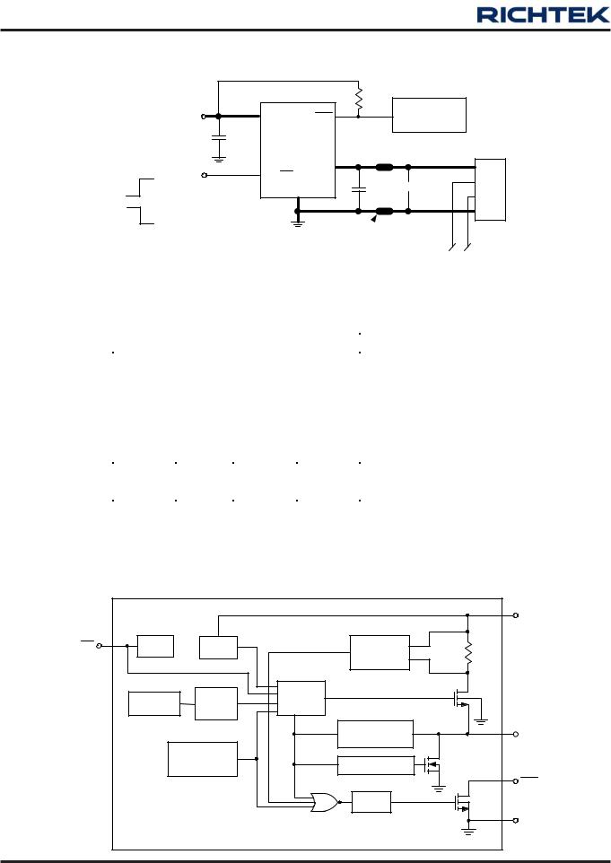
Typical Application Circuit
Pull-Up Resistor (10K to 100K) |
|||
Supply Voltage |
VIN |
FLG |
|
2.7V to 5.5V |
|||
|
|
||
CIN |
RT9715 |
|
|
1uF |
|
|
|
RT9715A/C/E/G |
VOUT |
||
Chip Enable |
|||
EN/EN |
COUT |
||
|
GND |
||
|
10uF |
||
RT9715B/D/F/H |
|
|
|
Chip Enable |
|
|
|
USB Controller
Over -Current
+  150uF
150uF
VBUS
D+
D- GND
Ferrite |
|
Beads |
Data |
|
Note : A low-ESR 150uF aluminum electrolytic or tantalum between VOUT and GND is strongly recommended to meet the 330mV maximum droop requirement in the hub VBUS. (see Application Information Section for further details)
Functional Pin Description
|
|
Pin No. |
|
|
|
|
|
|
|
|
SOT-23-5 |
SOT-23-5 |
SOT-23-5 |
SOP-8 / |
WDFN-8L |
|
Pin Name |
Pin Function |
|||
|
(G-Type) |
(R-Type) |
MSOP-8 |
3X3 |
|
|
|
|
|
|
1 |
1 |
5 |
6 , 7 , 8 |
6 , 7 , 8 |
|
VOUT |
Output Voltage. |
|||
2 |
2 |
2 |
1 |
1 |
GND |
Ground. |
||||
3 |
-- |
1 |
5 |
5 |
|
|
|
|
|
Fault FLAG Output. |
FLG |
||||||||||
4 |
4 |
3 |
4 |
4 |
|
|
|
Chip Enable (Active High/Low). |
||
EN/EN |
||||||||||
5 |
5 |
4 |
2 , 3 |
2 , 3 |
|
VIN |
Power Input Voltage. |
|||
-- |
3 |
-- |
-- |
-- |
|
NC |
No Internal Connection. |
|||
|
|
|
|
9 (Exposed |
|
|
|
|
|
The exposed pad must be soldered to a large |
-- |
-- |
-- |
-- |
|
|
|
|
|
PCB and connected to GND for maximum |
|
Pad) |
|
|
|
|
|
|||||
|
|
|
|
|
|
|
|
|
power dissipation. |
|
|
|
|
|
|
|
|
|
|
|
|
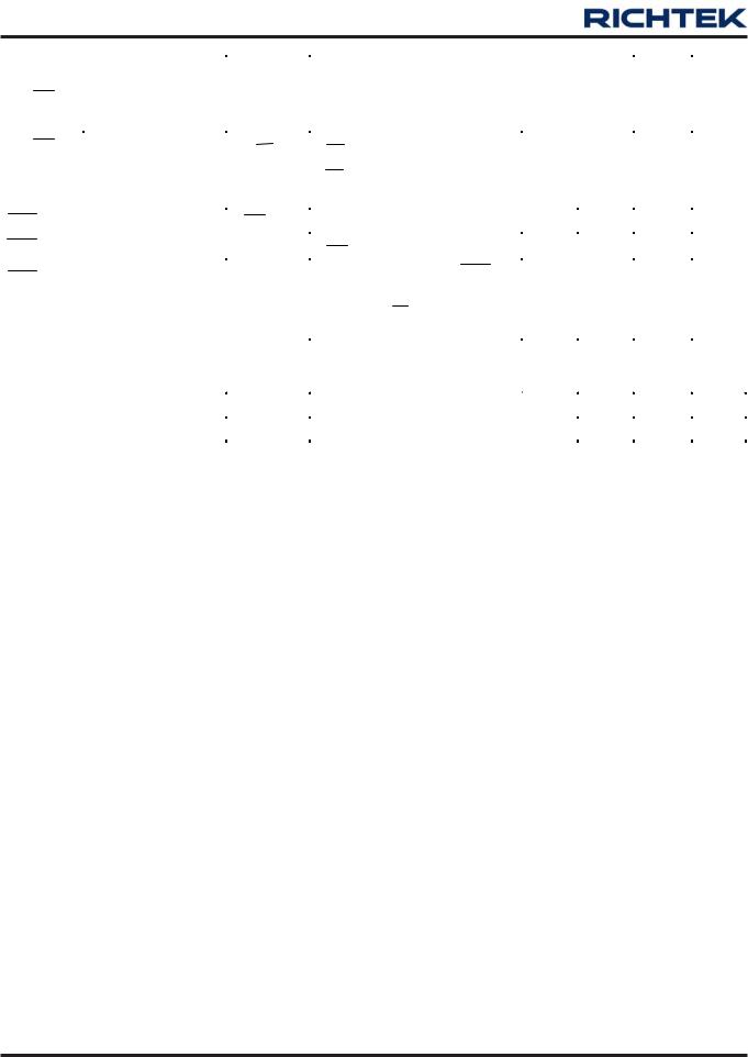
Function Block Diagram |
|
|
|
|
||
|
|
|
|
VIN |
|
|
EN/EN |
Bias |
UVLO |
Current |
|
|
|
|
|
|
Limiting |
|
|
|
|
Oscillator |
Charge |
Gate |
|
|
|
|
Control |
|
|
|
||
|
Pump |
|
|
|
||
|
|
|
|
|
|
|
|
|
|
Output Voltage |
VOUT |
|
|
|
|
|
Detection |
|
|
|
|
|
|
|
|
|
|
|
|
Thermal |
|
|
|
|
|
|
Protection |
Auto Discharge |
|
|
|
|
|
|
|
FLG |
|
|
|
|
|
Delay |
|
|
|
|
|
|
|
GND |
|
|
www.richtek.com |
|
|
|
DS9715-03 |
April |
2011 |
2

|
RT9715 |
Absolute Maximum Ratings (Note 1) |
|
z Supply Input Voltage, VIN -------------------------------------------------------------------------------------------- |
6V |
z EN Voltage -------------------------------------------------------------------------------------------------------------- |
−0.3V to 6V |
z FLAG Voltage ---------------------------------------------------------------------------------------------------------- |
6V |
z Power Dissipation, PD @ TA = 25°C |
|
SOT-23-5 ---------------------------------------------------------------------------------------------------------------- |
300mW |
SOP-8 -------------------------------------------------------------------------------------------------------------------- |
469mW |
MSOP-8 ----------------------------------------------------------------------------------------------------------------- |
469mW |
WDFN-8L 3x3 ---------------------------------------------------------------------------------------------------------- |
694mW |
z Package Thermal Resistance (Note 2) |
|
SOT-23-5, θJA ----------------------------------------------------------------------------------------------------------- |
250°C/W |
SOP-8, θJA -------------------------------------------------------------------------------------------------------------- |
160°C/W |
MSOP-8, θJA ------------------------------------------------------------------------------------------------------------ |
160°C/W |
WDFN-8L 3x3, θJA ----------------------------------------------------------------------------------------------------- |
108°C/W |
z Junction Temperature ------------------------------------------------------------------------------------------------- |
150°C |
z Lead Temperature (Soldering, 10 sec.) --------------------------------------------------------------------------- |
260°C |
z Storage Temperature Range ---------------------------------------------------------------------------------------- |
−65°C to 150°C |
z ESD Susceptibility (Note 3) |
|
HBM (Human Body Mode) ------------------------------------------------------------------------------------------ |
2kV |
MM (Machine Mode) -------------------------------------------------------------------------------------------------- |
200V |
Recommended Operating Conditions |
(Note 4) |
z Supply Input Voltage, VIN -------------------------------------------------------------------------------------------- |
2.7V to 5.5V |
z EN Voltage -------------------------------------------------------------------------------------------------------------- |
0V to 5.5V |
z Junction Temperature Range ---------------------------------------------------------------------------------------- |
−40°C to 100°C |
z Ambient Temperature Range ---------------------------------------------------------------------------------------- |
−40°C to 85°C |
Electrical Characteristics
(VIN = 5V, CIN = 1uF, COUT = 10uF, TA = 25°C, unless otherwise specified)
|
Parameter |
Symbol |
Test Conditions |
Min |
Typ |
Max |
Unit |
||
Input Quiescent Current |
IQ |
Switch On, VOUT = Open |
-- |
50 |
70 |
uA |
|||
Input Shutdown Current |
ISHDN |
Switch Off, VOUT = Open |
-- |
0.1 |
1 |
||||
|
|||||||||
|
|
RT9715A/B |
|
VIN = 5V, IOUT = 1.5A |
-- |
90 |
110 |
|
|
Switch On |
|
RT9715C/D |
RDS(ON) |
VIN = 5V, IOUT =1.3A |
-- |
90 |
110 |
mΩ |
|
Resistance |
|
RT9715E/F |
VIN = 5V, IOUT = 1A |
-- |
90 |
110 |
|||
|
|
|
|||||||
|
|
RT9715G/H |
|
VIN = 5V, IOUT = 0.6A |
-- |
90 |
110 |
|
|
|
|
RT9715A/B |
|
|
2 |
2.5 |
3.2 |
|
|
Current |
|
RT9715C/D |
ILIM |
VOUT = 4V |
1.5 |
2 |
2.8 |
A |
|
Limit |
|
RT9715E/F |
1.1 |
1.5 |
2.1 |
||||
|
|
|
|
||||||
|
|
RT9715G/H |
|
|
0.7 |
1 |
1.4 |
|
|
|
|
RT9715A/B |
|
|
-- |
1.7 |
-- |
|
|
Short |
|
RT9715C/D |
ISC_FB |
VOUT = 0V, Measured Prior to |
-- |
1.4 |
-- |
A |
|
Current |
|
RT9715E/F |
Thermal Shutdown |
-- |
1 |
-- |
|||
|
|
|
|||||||
|
|
RT9715G/H |
|
|
-- |
0.7 |
-- |
|
|
|
To be continued |
|
|
DS9715-03 April 2011 |
www.richtek.com |
3
RT9715
|
Parameter |
Symbol |
Test Conditions |
Min |
Typ |
Max |
Unit |
||
EN/EN |
|
Logic_High Voltage |
VIH |
VIN = 2.7V to 5.5V |
2 |
-- |
-- |
V |
|
Threshold |
|
Logic_Low Voltage |
VIL |
VIN = 2.7V to 5.5V |
-- |
-- |
0.8 |
V |
|
EN/EN Input Current |
IEN/EN |
VEN = 5V |
-- |
0.01 |
0.1 |
uA |
|||
Output Leakage Current |
ILEAKAGE |
VEN = 0V, RLOAD = 0Ω |
-- |
0.5 |
1 |
uA |
|||
Output Turn-On Rise Time |
TON_RISE |
10% to 90% of VOUT Rising |
-- |
200 |
-- |
us |
|||
FLG Output Resistance |
RFLG |
ISINK = 1mA |
-- |
20 |
-- |
Ω |
|||
FLG Off Current |
IFLG_OFF |
VFLG = 5V |
-- |
0.01 |
1 |
uA |
|||
FLG Delay Time |
TD |
From fault condition to FLG |
5 |
12 |
20 |
ms |
|||
assertion |
|||||||||
|
|
|
|
|
|
|
|
||
Shutdown Auto-Discharge |
RDischarge |
VEN = 0V, VEN = 5V |
-- |
100 |
150 |
Ω |
|||
Resistance |
|
||||||||
|
|
|
|
|
|
||||
Under-Voltage Lockout |
VUVLO |
VIN Rising |
1.3 |
1.7 |
-- |
V |
|||
Under-Voltage Hysteresis |
VUVLO |
VIN Decreasing |
-- |
0.1 |
-- |
V |
|||
Thermal Shutdown Protection |
TSD |
VOUT > 1V |
-- |
120 |
-- |
°C |
|||
VOUT = 0V |
-- |
100 |
-- |
°C |
|||||
|
|
|
|
||||||
Thermal Shutdown Hysteresis |
|
VOUT = 0V |
-- |
20 |
-- |
°C |
|||
Note 1. Stresses beyond those listed under “Absolute Maximum Ratings” may cause permanent damage to the device. These are stress ratings only, and functional operation of the device at these or any other conditions beyond those indicated in the operational sections of the specifications is not implied. Exposure to absolute maximum rating conditions for extended periods may affect device reliability.
Note 2. θJA is measured in the natural convection at TA = 25°C on a low effective single layer thermal conductivity test board of JEDEC 51-3 thermal measurement standard.
Note 3. Devices are ESD sensitive. Handling precaution is recommended.
Note 4. The device is not guaranteed to function outside its operating conditions.
www.richtek.com |
DS9715-03 April 2011 |
4

RT9715
Typical Operating Characteristics
On Resistance (mΩ)
108 |
|
|
|
On Resistance vs. Input Voltage |
|
|
||||||||||||
|
|
|
|
|
|
|
|
|
|
|
|
|
|
|
|
|||
|
|
IOUT = 2A |
|
|
|
|
|
|
|
|
|
|
|
|
||||
106 |
|
|
|
|
|
|
|
|
|
|
|
|
|
|
|
|
|
|
|
|
|
|
|
|
|
|
|
|
|
|
|
|
|
|
|
||
104 |
|
|
|
|
|
|
SOP-8 |
|
|
|
|
|
|
|
|
|
||
|
|
|
|
|
|
|
|
|
|
|
|
|
|
|
|
|
||
|
|
|
|
|
|
|
|
|
|
|
|
|
|
|
|
|
||
102 |
|
|
|
|
|
|
|
|
|
|
|
|
|
|
|
|
|
|
|
|
|
|
|
|
|
|
|
|
|
|
|
|
|
|
|
||
100 |
|
|
|
|
|
|
|
|
|
|
|
|
|
|
|
|
|
|
|
|
|
|
|
|
|
|
|
|
|
|
|
|
|
|
|
||
98 |
|
|
|
|
|
|
|
|
|
|
|
|
|
|
|
|
|
|
|
|
|
|
|
|
|
|
|
|
|
|
|
|
|
|
|
||
96 |
|
|
|
|
|
|
|
|
|
|
|
|
|
|
|
|
|
|
|
|
|
|
|
|
SOT-23-5 |
|
|
|
|
|
|
|
|
||||
|
|
|
|
|
|
|
|
|
|
|
|
|
|
|
||||
94 |
|
|
|
|
|
|
|
|
|
|
|
|
|
|
|
|
|
|
|
|
|
|
|
|
|
|
|
|
|
|
|
|
|
|
|
||
92 |
|
|
|
|
|
|
|
|
|
|
|
|
|
|
|
|
|
|
|
|
|
|
|
|
|
|
|
|
|
|
|
|
|
|
|
||
90 |
|
|
|
|
|
|
|
|
|
|
|
|
|
|
|
|
|
|
2.7 |
3.1 |
3.5 |
3.9 |
4.3 |
4.7 |
5.1 |
5.5 |
|||||||||||
|
||||||||||||||||||
Input Voltage (V)
On Resistance vs. Temperature
|
125 |
VIN = 5V, IOUT = 2A |
|
|
|
|
|
|||
|
120 |
|
|
|
|
|
|
|
|
|
Ω) |
115 |
|
|
|
|
|
|
|
|
|
110 |
|
|
|
|
|
|
|
|
|
|
(m |
105 |
|
|
|
|
|
|
|
|
|
Resistance |
|
|
|
SOP-8 |
|
|
|
|
||
100 |
|
|
|
|
|
|
|
|||
|
|
|
|
|
|
|
|
|
||
95 |
|
|
|
|
|
SOT-23-5 |
|
|
||
90 |
|
|
|
|
|
|
|
|||
|
|
|
|
|
|
|
|
|
||
85 |
|
|
|
|
|
|
|
|
|
|
On |
|
|
|
|
|
|
|
|
|
|
80 |
|
|
|
|
|
|
|
|
|
|
|
|
|
|
|
|
|
|
|
|
|
|
75 |
|
|
|
|
|
|
|
|
|
|
70 |
|
|
|
|
|
|
|
|
|
|
|
-40 |
-25 |
-10 |
5 |
20 |
35 |
50 |
65 |
80 |
Temperature (°C)
Quiescent Current vs. Input Voltage |
Quiescent Current vs. Temperature |
|
60 |
No Load |
|
|
|
|
|
|
|
60 |
|
|
|
|
|
|
|
|
|
|
|
|
58 |
|
|
|
|
|
|
|
VIN = 5V,No Load |
|
|
|
|
|
|
|
|||||
|
|
|
|
|
|
|
|
|
|
59 |
|
|
|
|
|
|
|
|
|
|
|
(uA) |
56 |
|
|
|
|
|
|
|
|
(uA) |
58 |
|
|
|
|
|
|
|
|
|
|
54 |
|
|
|
|
|
|
|
|
57 |
|
|
|
|
|
|
|
|
|
|
||
Current |
52 |
|
|
|
|
|
|
|
|
Current |
56 |
|
|
|
|
|
|
|
|
|
|
50 |
|
|
|
|
|
|
|
|
55 |
|
|
|
|
|
|
|
|
|
|
||
Quiescent |
48 |
|
|
|
|
|
|
|
|
Quiescent |
54 |
|
|
|
|
|
|
|
|
|
|
46 |
|
|
|
|
|
|
|
|
53 |
|
|
|
|
|
|
|
|
|
|
||
44 |
|
|
|
|
|
|
|
|
52 |
|
|
|
|
|
|
|
|
|
|
||
|
|
|
|
|
|
|
|
|
|
|
|
|
|
|
|
|
|
|
|
||
|
42 |
|
|
|
|
|
|
|
|
|
51 |
|
|
|
|
|
|
|
|
|
|
|
40 |
|
|
|
|
|
|
|
|
|
50 |
|
|
|
|
|
|
|
|
|
|
|
|
2.7 |
3.1 |
3.5 |
3.9 |
4.3 |
4.7 |
5.1 |
5.5 |
|
-40 |
-25 |
-10 |
5 |
20 |
35 |
50 |
65 |
80 |
95 |
110 |
Input Voltage (V) |
Temperature (°C) |
Shutdown Current (uA)
Shutdown Current vs. Input Voltage
1.0
No Load
0.9
0.8
0.7
0.6
0.5
0.4
0.3
0.2
0.1
0.0
2.7 |
3.1 |
3.5 |
3.9 |
4.3 |
4.7 |
5.1 |
5.5 |
Input Voltage (V)
Shutdown Current (uA)
Shutdown Current vs. Temperature
1.0
VIN = 5V
0.9
0.8
0.7
0.6
0.5
0.4
0.3
0.2
0.1
0.0
-40 -25 -10 5 20 35 50 65 80 95 110
Temperature (°C)
DS9715-03 April 2011 |
www.richtek.com |
5
 Loading...