


Richtek RT9293A-20GJ6, RT9293A-20GQWA, RT9293AGJ6, RT9293AGQW, RT9293AGQWA Schematic [ru]
...RT9293
Small Package, High Performance, Asynchronies Boost for 10 WLED Driver
General Description
The RT9293 is a high frequency, asynchronous boost converter. The internal MOSFET can support up to 10 White LEDs for backlighting and OLED power application, and the internal soft start function can reduce the inrush current. The device operates with 1-MHz fixed switching frequency to allow small external components and to simplify possible EMI problems. For the protection, the RT9293A provides 50V OVP and the RT9293B provides 50V/20V OVP to allow inexpensive and small-output capacitors with lower voltage ratings. The LED current is initially set with the external sense resistor RSET. The RT9293 is available in the tiny package type TSOT-23-6 and WDFN-8L 2x2 packages to provide the best solution for PCB space saving and total BOM cost.
Features
zVIN Operating Range : 2.5V to 5.5V
zInternal Power N-MOSFET Switch
zWide Range for PWM Dimming (100Hz to200kHz)
zMinimize the External Component Counts
zInternal Soft Start
zInternal Compensation
zUnder Voltage Protection
zOver Voltage Protection
zOver Temperature Protection
zSmall TSOT-23-6 and 8-Lead WDFN Packages
zRoHS Compliant and Halogen Free
Applications
zCellular Phones
zDigital Cameras
Ordering Information
RT9293 
 (-
(-

 )
)

Package Type
J6 : TSOT-23-6
QW : WDFN-8L 2x2 (W-Type)
Lead Plating System
G : Green (Halogen Free and Pb Free)
OVP Voltage
Default : 50V (RT9293A/B) 20 : 20V (RT9293B)
Feedback Voltage Reference A : 104mV
B : 300mV
Note :
Richtek products are :
`RoHS compliant and compatible with the current requirements of IPC/JEDEC J-STD-020.
`Suitable for use in SnPb or Pb-free soldering processes.
zPDAs and Smart Phones and MP3 and OLED.
zPortable Instruments
Pin Configurations
(TOP VIEW)
VIN VOUT EN
6 |
|
5 |
4 |
|
|
|
|
2 |
3 |
|
|
LX |
|
GND FB |
|||
TSOT-23-6 |
|
||||
GND |
1 |
GND |
8 |
LX |
|
VIN |
2 |
7 |
NC |
||
VOUT |
3 |
9 |
6 |
FB |
|
EN |
4 |
5 |
GND |
||
|
|||||
WDFN-8L 2x2
Marking Information
For marking information, contact our sales representative directly or through a Richtek distributor located in your area.
DS9293-01 April 2011 |
www.richtek.com |
1
RT9293
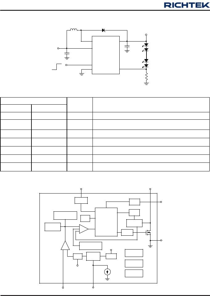
Typical Application Circuit
|
|
L |
|
D |
|
|
|
22µH to 47µH |
|
VOUT |
|||
|
|
|
|
|
||
|
|
|
LX |
VOUT |
|
|
|
VIN |
|
|
COUT |
|
|
|
CIN |
VIN |
1µF |
|
||
|
|
RT9293 |
10 WLEDs |
|||
|
|
2.2µF |
||||
|
|
|
|
|||
|
Chip Enable |
|
EN |
|
|
|
|
|
|
|
|
||
|
|
|
GND |
FB |
|
|
|
|
|
|
|
RSET |
|
Functional Pin Description |
|
|
|
|||
Pin No. |
Pin Name |
|
|
Pin Function |
||
RT9293□GJ6 |
RT9293□GQW |
|
|
|||
|
|
|
|
|||
1 |
8 |
LX |
Switching Pin. |
|
||
2 |
1, 5, |
GND |
Ground Pin. The exposed pad must be soldered to a large |
|||
9 (Exposed pad) |
PCB and connected to GND for maximum power dissipation. |
|||||
|
|
|||||
3 |
6 |
FB |
Feedback Pin, put a resistor to GND to setting the current. |
|||
4 |
4 |
EN |
Chip Enable (Active High). |
|||
5 |
3 |
VOUT |
Output Voltage Pin. |
|
||
6 |
2 |
VIN |
Input Supply. |
|
||
-- |
7 |
NC |
No Internal Connection. |
|
||
Function Block Diagram
|
|
VIN |
|
|
|
LX |
|
|
|
|
|
UVLO |
|
|
OVP |
VOUT |
|
|
|
|
|
|
|
|
|
|
|
||
Internal |
|
|
|
|
|
OCP |
|
|
|
|
|
|
|
|
|
|
|
|
|
Compensation |
|
OTP |
Logic Control, |
|
|
|
|
||
|
|
|
Current- |
|
|
|
|||
Internal |
|
|
PWM |
Minimum On |
|
|
|
||
|
- |
|
Time |
Sense |
|
|
|
||
Soft Start |
|
|
|
|
|
|
|
|
|
|
+ |
|
|
|
|
|
|
|
|
|
|
+ |
|
|
|
Driver |
|
|
|
|
|
|
|
|
|
|
|
|
|
EA |
|
|
|
|
|
|
GND |
|
|
GM |
|
|
Slope |
|
|
|
|
|
|
+ - |
|
Compensation |
Shutdown |
PWM |
|
|
|
||
|
|
|
Enable |
|
|
|
|
||
|
|
LPF |
20ms |
Oscillator |
|
|
|
||
|
|
Logic |
|
|
|
|
|
||
|
|
|
|
|
Reference |
|
|
|
|
|
|
|
|
|
|
|
|
|
|
|
VREF |
|
|
|
Voltage |
|
|
|
|
|
|
|
1µA |
Bias |
|
|
|
||
|
|
|
|
|
|
|
|
||
|
|
|
|
|
|
Current |
|
|
|
FB |
|
|
EN |
|
|
|
|
|
|
www.richtek.com |
|
|
|
|
|
|
DS9293-01 |
April |
2011 |
2 |
|
|
|
|
|
|
|
|
|

|
|
|
|
|
|
|
RT9293 |
|||
Absolute Maximum Ratings (Note 1) |
|
|
|
|
|
|
||||
z Supply Input Voltage, VIN ------------------------------------------------------------------------------------------------ |
|
|
|
|
−0.3V to 6V |
|||||
z Switching Pin, LX ---------------------------------------------------------------------------------------------------------- |
|
|
|
|
|
−0.3V to 50V |
||||
z VOUT ------------------------------------------------------------------------------------------------------------------------- |
|
|
|
|
|
−0.3V to 46V |
||||
z Other Pins------------------------------------------------------------------------------------------------------------------- |
|
|
|
|
|
−0.3V to 6V |
||||
z Power Dissipation, PD @ TA = 25°C |
|
|
|
|
|
|
|
|
||
TSOT-23-6 ------------------------------------------------------------------------------------------------------------------- |
|
|
|
|
|
0.392W |
|
|
||
WDFN−8L 2x2 -------------------------------------------------------------------------------------------------------------- |
|
|
|
|
|
0.606W |
|
|
||
z Package Thermal Resistance (Note 2) |
|
|
|
|
|
|
|
|||
TSOT-23-6, θJA ------------------------------------------------------------------------------------------------------------- |
|
|
|
|
|
255°C/W |
|
|
||
WDFN−8L 2x2, θJA -------------------------------------------------------------------------------------------------------- |
|
|
|
|
|
165°C/W |
|
|
||
WDFN−8L 2x2, θJC -------------------------------------------------------------------------------------------------------- |
|
|
|
|
|
20°C/W |
|
|
||
z Lead Temperature (Soldering, 10 sec.) ------------------------------------------------------------------------------- |
|
|
|
260°C |
|
|
||||
z Junction Temperature ----------------------------------------------------------------------------------------------------- |
|
|
|
|
|
150°C |
|
|
||
z Storage Temperature Range -------------------------------------------------------------------------------------------- |
|
|
|
|
−65°C to 150°C |
|||||
Recommended Operating Conditions (Note 3) |
|
|
|
|
|
|
||||
z Junction Temperature Range -------------------------------------------------------------------------------------------- |
|
|
|
|
−40°C to 125°C |
|||||
z Ambient Temperature Range -------------------------------------------------------------------------------------------- |
|
|
|
|
−40°C to 85°C |
|||||
Electrical Characteristics |
|
|
|
|
|
|
|
|||
(VIN = 3.7V, CIN = 2.2μF, COUT = 0.47μF, IOUT = 20mA, L = 22μH, TA = 25°C, unless otherwise specified) |
|
|
|
|
||||||
Parameter |
|
Symbol |
Test Conditions |
Min |
Typ |
Max |
|
Unit |
|
|
|
|
|
|
|
|
|
|
|
|
|
Input Voltage |
|
VIN |
|
2.5 |
-- |
5.5 |
|
V |
|
|
Under Voltage Lock Out |
VUVLO |
|
2 |
2.2 |
2.45 |
|
V |
|
||
|
|
|
|
|
|
|
|
|
|
|
UVLO Hysteresis |
|
|
|
-- |
0.1 |
-- |
|
V |
|
|
|
|
|
|
|
|
|
|
|
|
|
Quiescent Current |
|
IQ |
FB = 1.5V, No Switching |
-- |
400 |
600 |
|
μA |
|
|
Supply Current |
|
IIN |
FB = 0V, Switching |
-- |
1 |
2 |
|
mA |
|
|
|
|
|
|
|
|
|
|
|
|
|
Shutdown Current |
|
ISHDN |
VEN < 0.4V |
-- |
1 |
4 |
|
μA |
|
|
Line Regulation |
|
|
VIN = 3 to 4.3V |
-- |
1 |
-- |
|
% |
|
|
Load Regulation |
|
|
1mA to 20mA |
-- |
1 |
-- |
|
% |
|
|
|
|
|
|
|
|
|
|
|
|
|
Operation Frequency |
|
fOSC |
|
0.75 |
1 |
1.25 |
|
MHz |
|
|
Maximum Duty Cycle |
|
|
|
90 |
92 |
-- |
|
% |
|
|
|
|
|
|
|
|
|
|
|
|
|
Clock Rate |
|
|
|
0.1 |
-- |
200 |
|
kHz |
|
|
|
|
|
|
|
|
|
|
|
|
|
Feedback Reference |
RT9293A |
VREF |
|
94 |
104 |
114 |
|
mV |
|
|
Voltage |
|
RT9293B |
|
285 |
300 |
315 |
|
|
||
|
|
|
|
|
|
|
||||
|
|
|
|
|
|
|
|
|
|
|
On Resistance |
|
RDS(ON) |
|
-- |
0.7 |
1.2 |
|
Ω |
|
|
|
|
|
|
|
|
|
|
|
|
|
|
|
|
|
|
|
|
To be continued |
|||
|
|
|
|
|
|
|
|
|
|
|
DS9293-01 April 2011 |
|
|
|
|
|
www.richtek.com |
||||
3

RT9293
Parameter |
Symbol |
Test Conditions |
Min |
Typ |
Max |
Unit |
|
|
|
|
|
|
|
|
|
EN Threshold |
Logic-High |
VIH |
|
1.4 |
-- |
-- |
V |
Voltage |
Logic-Low |
VIL |
|
-- |
-- |
0.5 |
|
|
|
||||||
EN Sink Current |
|
IIH |
|
-- |
1 |
-- |
μ |
|
|
|
|
|
|
A |
|
EN Hysteresis |
|
|
|
-- |
0.1 |
-- |
V |
|
|
|
|
|
|
|
|
Over-Voltage |
OVP = 50V |
VOVP |
|
42 |
46 |
50 |
V |
Threshold |
RT9293B-20 |
|
16 |
17.5 |
20 |
||
|
|
|
|||||
|
|
|
|
|
|
|
|
Over-Current Threshold |
IOCP |
|
1 |
1.2 |
-- |
A |
|
OTP |
|
TOTP |
|
-- |
160 |
-- |
°C |
OTP Hysteresis |
|
|
|
-- |
30 |
-- |
°C |
Shutdown Delay |
|
TSHDN |
|
-- |
20 |
-- |
ms |
Note 1. Stresses listed as the above “Absolute Maximum Ratings” may cause permanent damage to the device. These are for stress ratings. Functional operation of the device at these or any other conditions beyond those indicated in the operational sections of the specifications is not implied. Exposure to absolute maximum rating conditions for extended periods may remain possibility to affect device reliability.
Note 2. θJA is measured in the natural convection at TA = 25°C on a low effective single layer thermal conductivity test board of JEDEC 51-3 thermal measurement standard. The case point of θJC is on the expose pad for the WDFN package.
Note 3. The device is not guaranteed to function outside its operating conditions.
www.richtek.com |
DS9293-01 April 2011 |
4

RT9293
Typical Operating Characteristics
Efficiency vs. Output Current
|
100 |
|
|
|
|
VIN = 4.5V |
|
|
90 |
|
|
|
|
||
|
|
|
|
|
|
|
|
|
80 |
|
|
|
|
VIN = 4V |
|
(%) |
70 |
|
|
|
|
|
|
60 |
|
|
|
|
|
|
|
Efficiency |
|
|
|
|
|
|
|
50 |
|
|
|
|
|
|
|
40 |
|
|
|
|
|
|
|
30 |
|
|
|
|
|
|
|
|
|
|
|
|
|
|
|
|
20 |
|
|
|
|
|
|
|
10 |
|
|
|
|
VOUT = 10V |
|
|
0 |
|
|
|
|
||
|
|
|
|
|
|
|
|
|
0 |
0.05 |
0.1 |
0.15 |
0.2 |
0.25 |
0.3 |
Efficiency vs. Input Voltage
|
100 |
|
|
|
|
|
|
|
90 |
|
|
|
|
ILOAD = 30mA |
|
|
|
|
|
|
|
|
|
|
80 |
|
|
|
|
ILOAD = 10mA |
|
|
70 |
|
|
|
|
||
(%) |
|
|
ILOAD = 20mA |
|
|
||
60 |
|
|
|
|
|||
|
|
|
|
|
|
||
Efficiency |
|
|
|
|
|
|
|
50 |
|
|
|
|
|
|
|
40 |
|
|
|
|
|
|
|
30 |
|
|
|
|
|
|
|
|
|
|
|
|
|
|
|
|
20 |
|
|
|
|
|
|
|
10 |
|
|
|
|
VOUT = 34V |
|
|
0 |
|
|
|
|
||
|
|
|
|
|
|
|
|
|
2.5 |
3 |
3.5 |
4 |
4.5 |
5 |
5.5 |
Output Current (A) |
Input Voltage (V) |
Output Voltage vs. Output Current |
Quiescent Current vs. Input Voltage |
|
40 |
|
|
|
|
|
|
|
|
500 |
|
35 |
|
|
|
|
|
|
|
Quiescent Current (µA) |
450 |
Output Voltage (V) |
30 |
|
|
|
|
|
|
|
400 |
|
25 |
|
|
|
|
|
|
|
350 |
||
20 |
|
|
|
|
|
|
|
300 |
||
15 |
|
|
|
|
|
|
|
250 |
||
|
|
|
|
|
|
|
|
|
||
|
10 |
|
|
|
|
VIN = 3.7V, VOUT = 34V |
200 |
|||
|
|
|
|
|
|
|
|
|
||
|
5 |
15 |
25 |
35 |
45 |
55 |
65 |
75 |
85 |
|
|
|
|
|
|
VFB = 1.5V |
|
2.5 |
3 |
3.5 |
4 |
4.5 |
5 |
5.5 |
Output Current (mA) |
Input Voltage (V) |
Frequency vs. Input Voltage |
Frequency vs. Temperature |
|
1100 |
|
|
|
|
|
|
1100 |
|
1050 |
|
|
|
|
|
|
1050 |
(kHz) |
1000 |
|
|
|
|
|
(kHz) |
1000 |
|
|
|
|
|
|
|
||
Frequency |
950 |
|
|
|
|
|
Frequency |
950 |
900 |
|
|
|
|
|
900 |
||
|
|
|
|
|
|
|
||
|
850 |
|
|
|
|
|
|
850 |
|
800 |
|
|
|
|
ILED = 20mA |
800 |
|
|
|
|
|
|
|
|
||
|
2.5 |
3 |
3.5 |
4 |
4.5 |
5 |
5.5 |
|
|
|
|
|
|
|
VIN = 3.7V, ILED = 20mA |
|||
-40 |
-25 |
-10 |
5 |
20 |
35 |
50 |
65 |
80 |
95 110 125 |
Input Voltage (V) |
Temperature (°C) |
|
|
DS9293-01 April 2011 |
www.richtek.com |
5
 Loading...