


Richtek RT9193-15GB, RT9193-15PB, RT9193-15PU5, RT9193-16GB, RT9193-16PB Schematic [ru]
...®
RT9193
300mA, Ultra-Low Noise, Ultra-Fast CMOS LDO Regulator
General Description
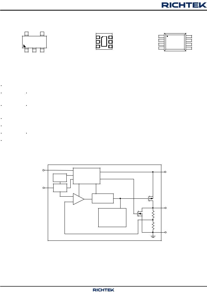
The RT9193 is designed for portable RF and wireless applications with demanding performance and space requirements. The RT9193 performance is optimized for battery-powered systems to deliver ultra low noise and low quiescent current. A noise bypass pin is available for further reduction of output noise. Regulator ground current increases only slightly in dropout, further prolonging the battery life. The RT9193 also works with low-ESR ceramic capacitors, reducing the amount of board space necessary for power applications, critical in hand-held wireless devices. The RT9193 consumes less than 0.01μA in shutdown mode and has fast turn-on time less than 50μs. The other features include ultra low dropout voltage, high output accuracy, current limiting protection, and high ripple rejection ratio. Available in the SC-70-5, SOT-23-5, TSOT-23-5, WDFN-6L 2x2 and MSOP-8 packages.
Ordering Information
RT9193-


Package Type
U5 : SC-70-5
B : SOT-23-5
J5 : TSOT-23-5
QW : WDFN-6L 2x2 (W-Type) F : MSOP-8
Lead Plating System P : Pb Free
G : Green (Halogen Free and Pb Free)
Output Voltage 15 : 1.5V
16 : 1.6V
:
49 : 4.9V
50 : 5.0V
1H : 1.85V
2H : 2.85V
4G : 4.75V
(1.5V to 5V with 0.1V step is available)
Note :
Richtek products are :
`RoHS compliant and compatible with the current requirements of IPC/JEDEC J-STD-020.
`Suitable for use in SnPb or Pb-free soldering processes.
Features
zUltra Low Noise for RF Application
zUltra Fast Response in Line/Load Transient
zQuick Start-Up (Typically 50μs)
z<0.01μA Standby Current When Shutdown
zLow Dropout : 220mV @ 300mA
zWide Operating Voltage Ranges : 2.5V to 5.5V
zTTL-Logic-Controlled Shutdown Input
zLow Temperature Coefficient
zCurrent Limiting Protection
zThermal Shutdown Protection
zOnly 1μF Output Capacitor Required for Stability
zHigh Power Supply Rejection Ratio
zCustom Voltage Available
zRoHS Compliant and 100% Lead (Pb)-Free
Applications
zCDMA/GSM Cellular Handsets
zBattery-Powered Equipment
zLaptop, Palmtops, Notebook Computers
zHand-Held Instruments
zPCMCIA Cards
zPortable Information Appliances
Marking Information
For marking information, contact our sales representative directly or through a Richtek distributor located in your area.
Typical Application Circuit
|
|
|
|
|
|
|
|
|
|
|
|
|
|
RT9193 |
|
|
|
|
|
|
|
|
|
VIN |
|
|
VIN |
VOUT |
|
|
|
|
|
|
VOUT |
||||||||||
|
|
|
|
|
|
|
|
|||||||||||||||
|
|
|
CIN |
|
|
|
|
|
|
|
|
|
|
|
|
COUT |
||||||
|
1µF/X7R |
|
|
|
|
GND |
|
|
|
|
|
|
|
1µF/X7R |
||||||||
|
|
|
|
|
|
|
|
|
|
|
|
|
|
|
|
|
|
|||||
|
|
|
|
|
|
|
|
|
|
|
|
|
|
|
|
|
|
|
|
|
|
|
|
|
|
|
|
|
|
|
|
|
|
|
|
|
|
|
|
|
|
|
|
|
|
Chip Enable |
EN |
BP |
|
|
|
|
CBP |
|||||||||||||||
|
|
|
|
|||||||||||||||||||
|
|
|
|
|
|
|
|
|
|
|
|
|
|
|
|
|
|
|
|
|||
|
|
|
|
|
|
|
|
|
|
|
|
|
|
|
|
|
|
|
|
|||
|
|
|
|
|
|
|
|
|
|
|
|
|
|
|
|
|
|
|
|
22nF |
||
|
|
|
|
|
|
|
|
|
|
|
|
|
|
|
|
|
|
|
|
|||
|
|
|
|
|
|
|
|
|
|
|
|
|
|
|
|
|
|
|
|
(Option for low noise) |
||
|
|
|
|
|
|
|
|
|
|
|
|
|
|
|
|
|
|
|
|
|||
|
|
|
|
|
|
|
|
|
|
|
|
|
|
|
|
|
|
|
|
|||
Copyright ©2013 Richtek Technology Corporation. All rights reserved. |
is a registered trademark of Richtek Technology Corporation. |
DS9193-16 January 2013 |
www.richtek.com |
|
1 |
RT9193 |
|
|
|
|
|
|
|
|
|
|
Pin Configurations |
(TOP VIEW) |
|
|
|
|
|||||
|
|
|
|
|
|
|||||
VOUT |
BP |
|
|
|
|
|
|
|
|
|
5 |
4 |
EN 1 |
|
6 |
BP |
NC |
|
8 |
NC |
|
|
|
GND 2 |
|
5 |
NC |
VIN |
2 |
7 |
EN |
|
|
|
7 |
NC |
3 |
6 |
BP |
||||
2 |
3 |
VIN 3 |
4 |
VOUT |
||||||
|
VOUT |
4 |
5 |
GND |
||||||
|
|
|
|
|
|
|||||
VIN GND EN |
WDFN-6L 2x2 |
MSOP-8 |
|
SC-70-5/SOT-23-5/TSOT-23-5
Functional Pin Description
Pin Name |
Pin Function |
|
|
|
|
EN |
Chip Enable (Active High). Note that this pin is high impedance. There should be a pull low 100kΩ |
|
resistor connected to GND when the control signal is floating. |
||
|
||
|
|
|
BP |
Reference Noise Bypass. This pin can be floating. For lowest noise performance, connect a 22nF |
|
capacitor between the BP and GND pins. |
||
|
||
|
|
|
GND |
Ground. |
|
|
|
|
VOUT |
Output Voltage. |
|
|
|
|
VIN |
Power Input Voltage. |
|
|
|
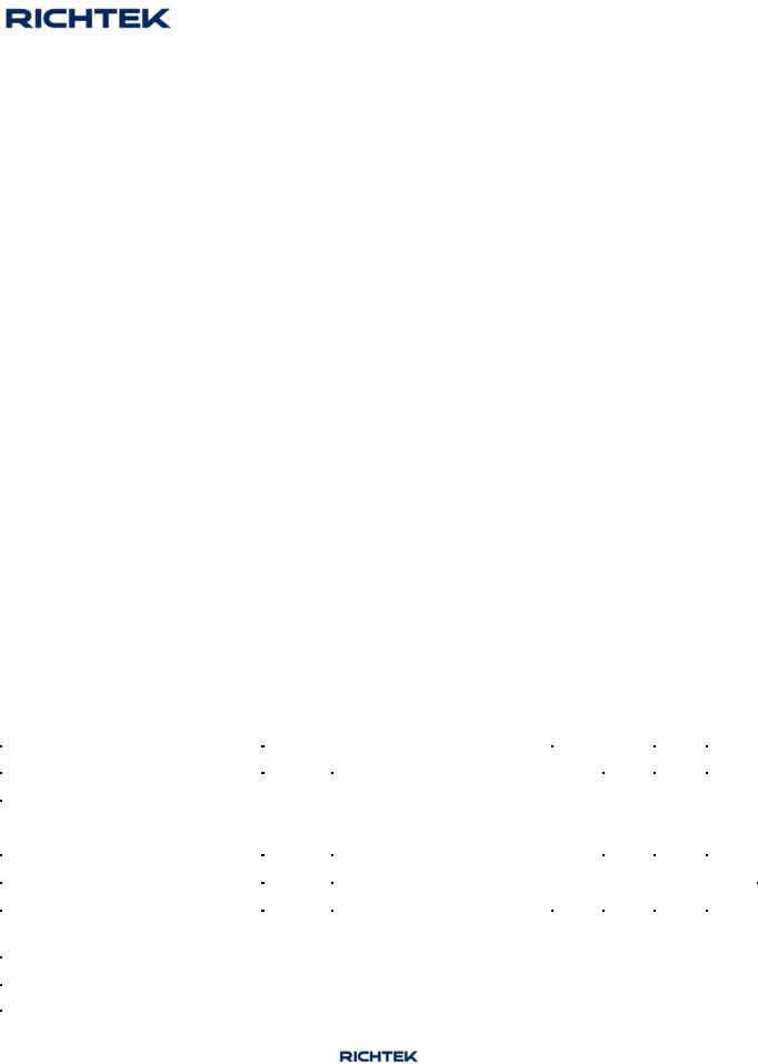
Function Block Diagram
EN |
|
Shutdown |
VIN |
|
Quick |
||
|
and |
|
|
|
Start |
Logic Control |
|
BP |
VREF |
|
|
|
|
+ |
MOSFET |
|
|
- |
Driver |
|
|
Error |
VOUT |
|
|
Amplifier |
|
|
|
|
Current-Limit |
|
|
|
and |
|
|
|
Thermal |
|
|
|
Protection |
|
|
|
GND |
Copyright ©2013 Richtek Technology Corporation. All rights reserved. |
is a registered trademark of Richtek Technology Corporation. |
www.richtek.com |
DS9193-16 January 2013 |
2
|
|
|
|
|
|
|
|
RT9193 |
|||
Absolute Maximum Ratings (Note 1) |
|
|
|
|
|
|
|
||||
z Supply Input Voltage ------------------------------------------------------------------------------------------------------ |
|
|
|
|
|
|
6V |
|
|||
z Power Dissipation, PD @ TA = 25°C |
|
|
|
|
|
|
|
|
|||
SC-70-5 ---------------------------------------------------------------------------------------------------------------------- |
|
|
|
|
|
|
|
300mW |
|
||
TSOT-23-5/SOT-23-5 ------------------------------------------------------------------------------------------------------ |
|
|
|
|
|
|
400mW |
|
|||
WDFN-6L 2x2 -------------------------------------------------------------------------------------------------------------- |
|
|
|
|
|
|
|
606mW |
|
||
MSOP-8 --------------------------------------------------------------------------------------------------------------------- |
|
|
|
|
|
|
|
625mW |
|
||
z Package Thermal Resistance |
(Note 2) |
|
|
|
|
|
|
|
|
||
SOT-70-5, θJA --------------------------------------------------------------------------------------------------------------- |
|
|
|
|
|
|
|
333°C/W |
|
||
TSOT-23-5/SOT-23-5, θJA ------------------------------------------------------------------------------------------------ |
|
|
|
|
|
|
250°C/W |
|
|||
TSOT-23-5/SOT-23-5, θJC ----------------------------------------------------------------------------------------------- |
|
|
|
|
|
|
25°C/W |
|
|||
WDFN-6L 2x2, θJA --------------------------------------------------------------------------------------------------------- |
|
|
|
|
|
|
|
165°C/W |
|
||
WDFN-6L 2x2, θJC |
-------------------------------------------------------------------------------------------------------- |
|
|
|
|
|
|
20°C/W |
|
||
MSOP-8 θJA ---------------------------------------------------------------------------------------------------------------- |
|
|
|
|
|
|
|
160°C/W |
|
||
MSOP-8 θJC ---------------------------------------------------------------------------------------------------------------- |
|
|
|
|
|
|
|
55°C/W |
|
||
z Junction Temperature ----------------------------------------------------------------------------------------------------- |
|
|
|
|
|
|
150°C |
|
|||
z Lead Temperature (Soldering, 10 sec.) ------------------------------------------------------------------------------- |
|
|
|
|
260°C |
|
|||||
z Storage Temperature Range -------------------------------------------------------------------------------------------- |
|
|
|
|
|
|
−65°C to 150°C |
||||
z ESD Susceptibility |
(Note 3) |
|
|
|
|
|
|
|
|
|
|
HBM (Human Body Model) ---------------------------------------------------------------------------------------------- |
|
|
|
|
|
|
2kV |
|
|||
MM (Machine Model) ----------------------------------------------------------------------------------------------------- |
|
|
|
|
|
|
200V |
|
|||
Recommended Operating Conditions |
(Note 4) |
|
|
|
|
|
|
||||
z Supply Input Voltage ------------------------------------------------------------------------------------------------------ |
|
|
|
|
|
|
2.5V to 5.5V |
||||
z EN Input Voltage ----------------------------------------------------------------------------------------------------------- |
|
|
|
|
|
|
|
0V to 5.5V |
|||
z Junction Temperature Range -------------------------------------------------------------------------------------------- |
|
|
|
|
|
|
−40°C to 125°C |
||||
z Ambient Temperature Range -------------------------------------------------------------------------------------------- |
|
|
|
|
|
|
−40°C to 85°C |
||||
Electrical Characteristics |
|
|
|
|
|
|
|
|
|||
(VIN = VOUT + 1V, CIN = COUT = 1μF, CBP = 22nF, TA = 25°C, unless otherwise specified) |
|
|
|
|
|
|
|||||
Parameter |
|
Symbol |
|
Test Conditions |
Min |
Typ |
|
Max |
|
Unit |
|
Output Voltage Accuracy |
|
VOUT |
IOUT = 1mA |
−2 |
-- |
|
2 |
|
% |
||
Current Limit |
|
|
ILIM |
RLOAD = 1Ω |
360 |
400 |
|
-- |
|
mA |
|
Quiescent Current |
|
|
IQ |
VEN |
≥ 1.2V, IOUT = 0mA |
-- |
90 |
|
130 |
|
μA |
Dropout Voltage |
(Note 5) |
|
VDROP |
IOUT = 200mA, VOUT > 2.8V |
|
170 |
|
200 |
|
mV |
|
|
IOUT = 300mA, VOUT > 2.8V |
-- |
220 |
|
300 |
|
|||||
|
|
|
|
|
|
|
|||||
Line Regulation |
|
|
VLINE |
VIN = (VOUT + 1V) to 5.5V, |
-- |
-- |
|
0.3 |
|
% |
|
|
|
IOUT = 1mA |
|
|
|||||||
|
|
|
|
|
|
|
|
|
|
||
Load Regulation |
|
|
VLOAD |
1mA < IOUT < 300mA |
-- |
-- |
|
0.6 |
|
% |
|
Standby Current |
|
|
ISTBY |
VEN = GND, Shutdown |
-- |
0.01 |
|
1 |
|
μA |
|
|
|
|
|
|
|
|
|
|
|
|
|
Copyright ©2013 Richtek Technology Corporation. All rights reserved. |
|
is a registered trademark of Richtek Technology Corporation. |
|
||||||||
DS9193-16 January |
2013 |
|
|
|
|
|
|
|
www.richtek.com |
||
3
RT9193
Parameter |
|
Symbol |
Test Conditions |
Min |
Typ |
Max |
Unit |
|
|
|
|
|
|
|
|
|
|
EN Input Bias Current |
|
IIBSD |
VEN = GND or VIN |
-- |
0 |
100 |
nA |
|
EN Threshold |
|
Logic-Low |
VIL |
VIN = 3V to 5.5V, Shutdown |
-- |
-- |
0.4 |
V |
Voltage |
|
Logic-High |
VIH |
VIN = 3V to 5.5V, Start-Up |
1.2 |
-- |
-- |
|
|
|
|||||||
Output Noise Voltage |
|
eNO |
10Hz to 100kHz, IOUT = 200mA |
-- |
100 |
-- |
μVRMS |
|
|
COUT = 1μF |
|||||||
|
|
|
|
|
|
|
|
|
Power Supply |
|
f = 100Hz |
PSRR |
COUT = 1μF, IOUT = 10mA |
-- |
−70 |
-- |
dB |
Rejection Rate |
|
f = 10kHz |
-- |
−50 |
-- |
|||
|
|
|
|
|||||
Thermal Shutdown Temperature |
TSD |
|
-- |
165 |
-- |
°C |
||
Thermal Shutdown Temperature |
TSD |
|
-- |
30 |
-- |
°C |
||
|
|
|
|
|
|
|
|
|
Note 1. Stresses beyond those listed “Absolute Maximum Ratings” may cause permanent damage to the device. These are stress ratings only, and functional operation of the device at these or any other conditions beyond those indicated in the operational sections of the specifications is not implied. Exposure to absolute maximum rating conditions may affect device reliability.
Note 2. θJA is measured at TA = 25°C on a low effective thermal conductivity single-layer test board per JEDEC 51-3. Note 3. Devices are ESD sensitive. Handling precaution is recommended.
Note 4. The device is not guaranteed to function outside its operating conditions.
Note 5. The dropout voltage is defined as VIN − VOUT, which is measured when VOUT is VOUT(NORMAL) − 100mV.
Copyright ©2013 Richtek Technology Corporation. All rights reserved. |
is a registered trademark of Richtek Technology Corporation. |
www.richtek.com |
DS9193-16 January 2013 |
4

RT9193
Typical Operating Characteristics
Output Voltage vs. Temperature
|
1.8 |
RT9193-15xU5 |
|
|
|
|
|
||
|
|
|
|
|
|
|
|||
|
|
VIN = 3.3V |
|
|
|
|
|
|
|
|
1.7 |
CIN = COUT = 1μF X7R |
|
|
|
|
|||
(V) |
1.6 |
|
|
|
|
|
|
|
|
Voltage |
|
|
|
|
|
|
|
|
|
1.5 |
|
|
|
|
|
|
|
|
|
|
|
|
|
|
|
|
|
|
|
Output |
1.4 |
|
|
|
|
|
|
|
|
|
|
|
|
|
|
|
|
|
|
|
1.3 |
|
|
|
|
|
|
|
|
|
1.2 |
|
|
|
|
|
|
|
|
|
|
-50 |
-25 |
0 |
25 |
50 |
75 |
100 |
125 |
Temperature (°C)
Quiescent Current vs. Temperature
|
95 |
RT9193-15xU5 |
|
|
|
|
|
||
|
|
|
|
|
|
|
|||
|
90 |
VIN = 3.3V |
|
|
|
|
|
|
|
(µA) |
CIN = COUT = 1μF X7R |
|
|
|
|
||||
|
|
|
|
|
|||||
85 |
|
|
|
|
|
|
|
|
|
Current |
|
|
|
|
|
|
|
|
|
80 |
|
|
|
|
|
|
|
|
|
|
|
|
|
|
|
|
|
|
|
Quiescent |
75 |
|
|
|
|
|
|
|
|
70 |
|
|
|
|
|
|
|
|
|
|
|
|
|
|
|
|
|
|
|
|
65 |
|
|
|
|
|
|
|
|
|
60 |
|
|
|
|
|
|
|
|
|
|
-50 |
-25 |
0 |
25 |
50 |
75 |
100 |
125 |
Temperature (°C)
|
300 |
Dropout Voltage vs. Load Current |
|
|
20 |
|
|
PSRR |
|
|
|||||
|
RT9193-33xB |
|
|
|
|
|
|
VIN = 4V to 5V |
|
|
|
|
|||
|
|
|
|
|
|
|
|
|
|
|
|
|
|||
|
250 |
CIN = COUT = 1μF |
|
TJ = 125°C |
|
|
|
CIN = COUT = 1μF, X7R |
|
|
|
||||
(mV) |
|
|
|
|
|
0 |
|
|
|
|
|
|
|||
200 |
|
|
|
|
|
|
PSRR (dB) |
|
|
|
|
|
|
|
|
Dropout Voltage |
|
|
|
|
|
|
-20 |
|
|
|
|
|
|
||
|
|
TJ = 25°C |
|
|
|
|
|
|
|
|
|
||||
150 |
|
|
|
|
|
|
|
|
|
|
|
||||
|
|
|
|
|
|
|
|
|
|
|
|
|
|||
|
|
|
|
|
TJ = -40°C |
|
-40 |
|
|
|
|
|
|
||
100 |
|
|
|
|
|
|
|
|
|
|
|
|
|||
|
|
|
|
|
|
|
|
|
ILoad = 100mA |
|
|
||||
|
|
|
|
|
|
|
-60 |
|
|
|
|
||||
50 |
|
|
|
|
|
|
|
|
|
|
ILoad = 10mA |
|
|||
|
|
|
|
|
|
|
|
|
|
|
|
|
|
||
|
0 |
|
|
|
|
|
|
|
-80 |
10 |
100 |
1K |
10K |
100K |
1M |
|
0 |
0.05 |
0.1 |
0.15 |
0.2 |
0.25 |
0.3 |
|
|
||||||
|
|
|
0.01 |
0.1 |
1 |
10 |
100 |
1000 |
|||||||
Load Current (A) |
Frequency (kHz) |
EN Pin Shutdown Threshold vs. Temperature |
EN Pin Shutdown Response |
|
1.75 |
RT9193-15xU5 |
|
|
|
|
|
EN Pin Voltage |
|
|
VIN = 5V |
RT9193-28xU5 |
||
Threshold (V) |
|
|
|
|
|
|
|
|
||||||
|
VIN = 3.3V |
|
|
|
|
|
|
|
10 |
CIN = COUT = 1μF |
No Load |
|||
1.50 |
CIN = COUT = 1μF X7R |
|
|
|
|
(V) |
||||||||
|
|
|
|
|
|
|
|
5 |
|
|
||||
|
|
|
|
|
|
|
|
|
|
|
||||
1.25 |
|
|
|
|
|
|
|
|
0 |
|
|
|||
|
|
|
|
|
|
|
|
|
|
|
||||
|
|
|
|
|
|
|
|
|
|
|
|
|||
EN Pin Shutdown |
1.00 |
|
|
|
|
|
|
|
|
Output Voltage |
|
2 |
|
|
|
|
|
|
|
|
|
|
|
|
|
|
|||
0.75 |
|
|
|
|
|
|
|
|
(V) |
1 |
|
|
||
|
|
|
|
|
|
|
|
|
|
|
||||
|
|
|
|
|
|
|
|
|
0 |
|
|
|||
|
|
|
|
|
|
|
|
|
|
|
|
|||
|
0.50 |
|
|
|
|
|
|
|
|
|
|
|
|
|
|
|
-50 |
-25 |
0 |
25 |
50 |
75 |
100 |
125 |
|
|
|
Time (500μs/Div) |
|
Temperature (°C)
Copyright ©2013 Richtek Technology Corporation. All rights reserved. |
is a registered trademark of Richtek Technology Corporation. |
DS9193-16 January 2013 |
www.richtek.com |
5
 Loading...