


Richtek RT9166-12GVL, RT9166-12PVL, RT9166-12PX, RT9166-12PXL, RT9166-13GVL Schematic [ru]
...®
RT9166/A
300/600mA, Ultra-Fast Transient Response LDO Regulator
General Description
The RT9166/A series are CMOS low dropout regulators optimized for ultra-fast transient response. The devices are capable of supplying 300mAor 600mA of output current with a dropout voltage of 230mV or 580mV respectively.
The RT9166/A series are is optimized for CD/DVD-ROM, CD/RW or wireless communication supply applications. The RT9166/A regulators are stable with output capacitors as low as 1μF. The other features include ultra low dropout voltage, high output accuracy, current limiting protection, and high ripple rejection ratio.
The devices are available in fixed output voltages range of 1.2V to 4.5V with 0.1V per step. The RT9166/A regulators are available in 3-lead SOT-23 (RT9166 only), SOT-89, SOT-223, TO-92 and TO-252 packages.
Features
zLow Quiescent Current (Typically 220μA)
zGuaranteed 300/600mA Output Current
zLow Dropout Voltage : 230/580mV at 300/600mA
zWide Operating Voltage Ranges : 3V to 5.5V
zUltra-Fast Transient Response
zTight Load and Line Regulation
zCurrent Limiting Protection
zThermal Shutdown Protection
zOnly Low-ESR Ceramic Capacitor Required for Stability
zCustom Voltage Available
zRoHS Compliant and 100% Lead (Pb)-Free
Applications
z CD/DVD-ROM, CD/RW
Ordering Information
RT9166/A-


Package Type
VL : SOT-23-3 (L-Type) (RT9166 Only)
X : SOT-89
XL : SOT-89 (L-Type)
G : SOT-223
GL : SOT-223 (L-Type)
Z : TO-92
L : TO-252
Lead Plating System
P : Pb Free
G : Green (Halogen Free and Pb Free)
Output Voltage 12 : 1.2V
13 : 1.3V
:
45 : 4.5V
1B : 1.25V
600mA Output Current
300mA Output Current
Note :
Richtek products are :
`RoHS compliant and compatible with the current requirements of IPC/JEDEC J-STD-020.
`Suitable for use in SnPb or Pb-free soldering processes.
zWireless LAN Card/Keyboard/Mouse
zBattery-Powered Equipment
zXDSL Router
zPCMCIA Card
Marking Information
For marking information, contact our sales representative directly or through a Richtek distributor located in your area.
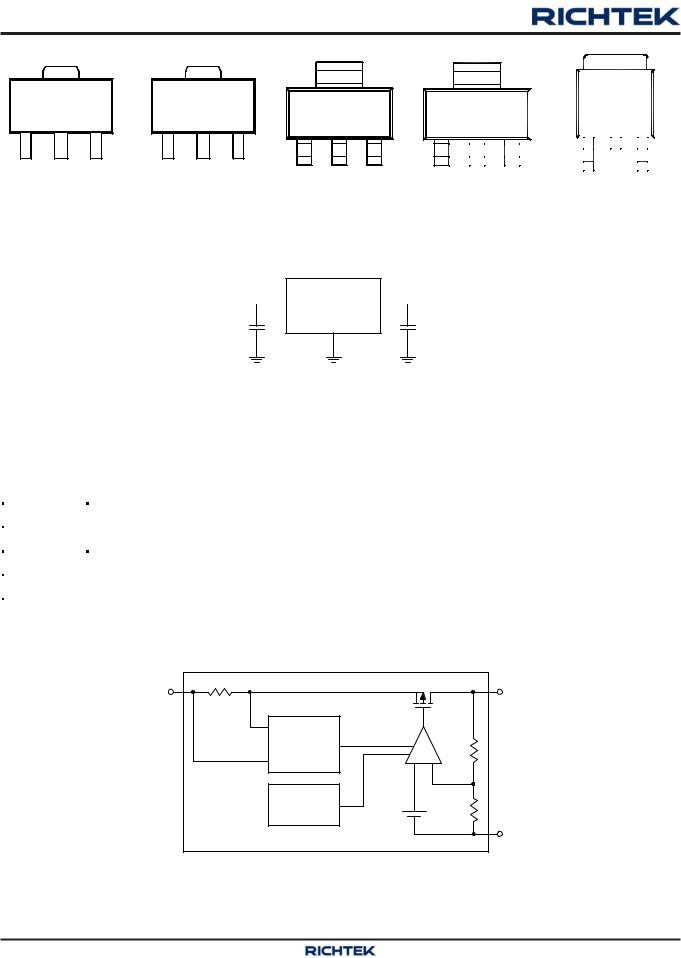
Pin Configurations
(TOP VIEW)
VIN
3
2
GND VOUT
SOT-23-3 (L-Type) (RT9166)
3 
 VOUT 2
 GND 1
GND 1 
 VIN
VIN
TO-92
Copyright ©2012 Richtek Technology Corporation. All rights reserved. |
is a registered trademark of Richtek Technology Corporation. |
DS9166/A-23 June 2012 |
www.richtek.com |
|
1 |
RT9166/A
1 |
2 |
3 |
VOUT GND VIN (TAB)
SOT-89
1 |
2 |
3 |
GND VIN VOUT (TAB)
SOT-89 (L-Type)
Typical Application Circuit
VIN 
CIN
1uF
|
|
|
|
|
|
|
|
|
|
|
|
|
|
|
|
|
|
|
|
|
|
|
|
|
|
|
|
|
|
|
|
|
|
|
|
|
|
|
|
|
|
1 |
2 |
3 |
1 |
|
2 |
|
3 |
|
|
1 |
|
2 |
|
3 |
|
|||||
|
|
|
|
|
|
|
||||||||||||||
|
|
|
|
|
|
|
|
|
|
|
|
|
|
|
|
|
|
|
|
|
|
|
|
|
|
|
|
|
|
|
|
|
|
|
|
|
|
|
|
|
|
|
|
|
|
|
|
|
|
|
|
|
|
|
|
|
|
|
|
|
|
|
|
|
|
|
|
|
|
|
|
|
|
|
|
|
|
GND |
|
|
|
||
|
|
|
|
|
|
|
|
|
|
|
|
|
|
|
|
|
|
|||
|
|
|
|
|
|
|
|
|
|
|
|
|
|
|
|
|
|
|
|
|
VOUT |
GND |
VIN |
GND |
VIN |
VOUT |
|
|
|
|
|
|
|
|
|
|
|||||
VOUT |
|
|
|
VIN |
||||||||||||||||
|
(TAB) |
|
|
|
(TAB) |
|
|
|
|
|
|
|||||||||
|
|
|
|
|
|
|
|
|
|
|
|
|
|
|
|
|
||||
SOT-223 |
|
SOT-223 (L-Type) |
|
|
|
TO-252 |
||||||||||||||
RT9166/A |
|
|
VIN |
VOUT |
VOUT |
|
GND |
COUT |
|
|
1uF |
Note: To prevent oscillation, a 1μF minimum X7R or X5R dielectric is strongly recommended if ceramics are used as input/output capacitors. When using the Y5V dielectric, the minimum value of the input/output capacitance that can be used for stable over full operating temperature range is 3.3μF. (see Application Information Section for further details)
Functional Pin Description
Pin Name |
Pin Function |
VIN |
Supply Input. |
VOUT |
Regulator Output. |
|
|
GND |
Common Ground. |
Function Block Diagram
VIN |
|
VOUT |
|
Current |
Error |
|
|
Amplifier |
|
||
Limiting |
|
||
- |
+ |
||
Sensor |
|||
Thermal |
1.2V |
|
|
Shutdown |
|
||
Reference |
|
||
|
GND |
||
|
|
Copyright ©2012 Richtek Technology Corporation. All rights reserved. |
is a registered trademark of Richtek Technology Corporation. |
www.richtek.com |
DS9166/A-23 June 2012 |
2
|
RT9166/A |
Absolute Maximum Ratings (Note 1) |
|
z Supply Input Voltage ------------------------------------------------------------------------------------------------- |
6.5V |
z Power Dissipation, PD @ TA = 25°C |
|
SOT-23-3 --------------------------------------------------------------------------------------------------------------- |
0.4W |
SOT-89 ------------------------------------------------------------------------------------------------------------------ |
0.571W |
SOT-223 ---------------------------------------------------------------------------------------------------------------- |
0.740W |
TO-252 ------------------------------------------------------------------------------------------------------------------ |
1.470W |
z Package Thermal Resistance (Note 2) |
|
SOT-23-3, θJA ---------------------------------------------------------------------------------------------------------- |
250°C/W |
SOT-89, θJA ------------------------------------------------------------------------------------------------------------ |
175°C/W |
SOT-89, θJC ------------------------------------------------------------------------------------------------------------ |
58°C/W |
SOT-223, θJA ----------------------------------------------------------------------------------------------------------- |
135°C/W |
SOT-223, θJC ---------------------------------------------------------------------------------------------------------- |
15°C/W |
TO-252, θJA ------------------------------------------------------------------------------------------------------------ |
68°C/W |
TO-252, θJC ------------------------------------------------------------------------------------------------------------ |
7°C/W |
z Lead Temperature (Soldering, 10 sec.) -------------------------------------------------------------------------- |
260°C |
z Junction Temperature ------------------------------------------------------------------------------------------------ |
150°C |
z Storage Temperature Range --------------------------------------------------------------------------------------- |
−65°C to 150°C |
z ESD Susceptibility (Note 3) |
|
HBM (Human Body Model) ----------------------------------------------------------------------------------------- |
2kV |
Recommended Operating Conditions |
(Note 4) |
z Supply Input Voltage ------------------------------------------------------------------------------------------------- |
2.8V to 5.5V |
z Junction Temperature Range --------------------------------------------------------------------------------------- |
− 40°C to 125°C |
z Ambient Temperature Range --------------------------------------------------------------------------------------- |
−40°C to 85°C |
Electrical Characteristics
(VIN = VOUT + 1V or VIN = 2.8V whichever is greater, CIN = 1μF, COUT = 1μF, TA = 25°C, unless otherwise specified)
|
Parameter |
Symbol |
|
Test Conditions |
Min |
Typ |
Max |
|
Unit |
||
|
Output Voltage Accuracy |
VOUT |
|
IOUT = 1mA |
−1 |
-- |
3 |
|
% |
||
|
Current Limit |
|
RT9166 |
ILIM |
|
RLOAD = 1Ω |
300 |
-- |
-- |
|
mA |
|
|
|
|
|
|
|
|
||||
|
|
RT9166A |
|
600 |
-- |
-- |
|
||||
|
|
|
|
|
|
|
|
||||
|
|
|
|
|
|
|
|
|
|
|
|
|
Quiescent Current |
(Note 5) |
IQ |
|
IOUT = 0mA |
-- |
220 |
300 |
|
μA |
|
|
Dropout Voltage |
|
RT9166 |
VDROP |
|
IOUT = 300mA |
-- |
230 |
-- |
|
mV |
|
(Note 6) |
|
RT9166A |
|
IOUT = 600mA |
-- |
580 |
-- |
|
||
|
|
|
|
|
|
||||||
|
Line Regulation |
|
|
VLINE |
|
VIN = (VOUT + 0.3V) to 5.5V, |
-- |
0.2 |
-- |
|
%/V |
|
|
|
|
IOUT = 1mA |
|
||||||
|
|
|
|
|
|
|
|
|
|
|
|
|
Load Regulation |
|
RT9166 |
VLOAD |
|
1mA < IOUT < 300mA |
-- |
15 |
35 |
|
mV |
|
(Note 7) |
|
RT9166A |
|
1mA < IOUT < 600mA |
-- |
30 |
55 |
|
||
|
|
|
|
|
|
||||||
|
Power Supply Rejection Rate |
PSRR |
f = 1kHz, COUT = 1μF |
-- |
−55 |
-- |
|
dB |
|||
|
Thermal Shutdown Temperature |
TSD |
|
|
-- |
170 |
-- |
|
°C |
||
|
Thermal Shutdown Hysteresis |
TSD |
|
|
-- |
40 |
-- |
|
°C |
||
|
|
|
|
|
|
|
|
|
|
|
|
Copyright ©2012 Richtek Technology Corporation. All rights reserved. |
is a registered trademark of Richtek Technology Corporation. |
|
|||||||||
DS9166/A-23 June |
2012 |
|
|
|
|
|
|
www.richtek.com |
|||
3
RT9166/A
Note 1. Stresses beyond those listed “Absolute Maximum Ratings” may cause permanent damage to the device. These are stress ratings only, and functional operation of the device at these or any other conditions beyond those indicated in the operational sections of the specifications is not implied. Exposure to absolute maximum rating conditions may affect device reliability.
Note 2. θJA is measured at TA = 25°C on a low effective thermal conductivity single-layer test board per JEDEC 51-3. Note 3. Devices are ESD sensitive. Handling precaution is recommended.
Note 4. The device is not guaranteed to function outside its operating conditions.
Note 5. Quiescent, or ground current, is the difference between input and output currents. It is defined by IQ = IIN - IOUT under no load condition (IOUT = 0mA). The total current drawn from the supply is the sum of the load current plus the ground pin current.
Note 6.The dropout voltage is defined as VIN − VOUT, which is measured when VOUT is VOUT(NORMAL) − 100mV.
Note 7. Regulation is measured at constant junction temperature by using a 20ms current pulse. Devices are tested for load regulation in the load range from 1mA to 300mA and 600mA respectively.
Copyright ©2012 Richtek Technology Corporation. All rights reserved. |
is a registered trademark of Richtek Technology Corporation. |
www.richtek.com |
DS9166/A-23 June 2012 |
4

RT9166/A
Typical Operating Characteristics
Dropout Voltage vs. Load Current
|
700 |
CIN = 1uF |
|
|
|
|
|
|
|
|
|
|
TJ = 125°C |
|
|
|
600 |
COUT = 1uF |
|
|
|
|
|
(mV) |
|
|
|
|
|
|
|
500 |
|
|
TJ = 25°C |
|
|
||
Voltage |
|
|
|
|
|
||
400 |
|
|
|
|
|
|
|
300 |
|
|
|
|
|
|
|
Dropout |
|
|
|
|
|
|
|
200 |
|
|
|
|
TJ = −40°C |
||
|
|
|
|
|
|
||
|
|
|
|
|
|
|
|
|
100 |
|
|
|
|
|
|
|
0 |
|
|
|
|
|
|
|
0 |
100 |
200 |
300 |
400 |
500 |
600 |
Power Supply Rejection Ratio
|
0 |
VIN = 5V |
|
|
|
|
|
|
|
|
|
|
|
|
-10 |
CIN = 1uF |
|
|
|
|
|
COUT = 1uF |
|
|
|
|
|
|
|
|
|
|
|
|
(dB) |
-20 |
|
|
|
|
|
-30 |
|
|
|
|
|
|
PSRR |
|
|
|
|
|
|
-40 |
100mA |
|
|
|
|
|
|
|
|
|
|
||
|
|
|
|
|
|
|
|
|
|
1mA |
|
|
|
|
-50 |
|
|
|
|
|
|
-60 |
|
|
|
|
|
|
10 |
100 |
1k |
10k |
100k |
1M |
Load Current (mA) |
Frequency (Hz) |
Region of Stable COUT ESR vs. Load Current |
Output Noise |
|
100.00 |
|
|
|
COUT = 1uF to 4.7uF |
|
VIN = 5V |
ILOAD = 100mA |
||
|
|
|
|
|
|
|||||
|
|
|
|
|
|
|
|
(μV) |
CIN = 1uF |
COUT = 1uF |
|
10.00 |
|
|
Instable |
|
|
|
400 |
|
|
|
|
|
|
|
|
|
|
|||
ESR (Ω) |
1.00 |
|
|
|
|
|
|
Signal |
200 |
|
|
|
|
|
|
|
|
|
|||
|
|
|
Stable |
|
|
|
0 |
|
||
|
|
|
|
|
|
|
|
|||
OUT |
|
|
|
|
|
|
Noise |
|
|
|
0.10 |
|
|
|
|
|
|
-200 |
|
||
C |
0.01 |
|
|
Instable |
|
|
|
Output |
-400 |
|
|
|
|
|
|
|
|
||||
|
|
|
|
|
|
|
|
|
f = 10Hz to 100KHz |
|
|
0.00 |
|
|
|
|
|
|
|
Time (1ms/DIV) |
|
|
0 |
100 |
200 |
300 |
400 |
500 |
600 |
|
|
|
Load Current (mA)
Current Limit vs. Input voltage |
Current Limit vs. Input voltage |
|
900 |
|
|
|
|
|
|
900 |
|
|
|
|
|
Limit (mA) |
850 |
|
|
|
|
|
Limit (mA) |
850 |
|
|
|
|
|
800 |
|
|
|
|
|
800 |
|
|
|
|
|
||
Current |
750 |
VIN = 5V |
|
|
|
|
Current |
750 |
VIN = 5V |
|
|
|
|
|
|
|
|
|
|
|
|
|
|
||||
|
|
CIN = 1uF |
|
|
|
|
|
|
CIN = 1uF |
|
|
|
|
|
|
COUT = 1uF |
|
|
|
|
|
|
COUT = 1uF |
|
|
|
|
|
700 |
RL = 0.5Ω |
|
|
RT9166-33xX |
|
700 |
RL = 0.5Ω |
|
|
RT9166-33xVL |
||
|
|
|
|
|
|
|
|
|
|
|
|
||
|
3 |
3.5 |
4 |
4.5 |
5 |
5.5 |
|
3 |
3.5 |
4 |
4.5 |
5 |
5.5 |
Input voltage (V) |
Input voltage (V) |
|
|
Copyright ©2012 Richtek Technology Corporation. All rights reserved. |
is a registered trademark of Richtek Technology Corporation. |
DS9166/A-23 June 2012 |
www.richtek.com |
5
 Loading...