


Richtek RT9161-15PX, RT9161-18PV, RT9161-18PX, RT9161-20PV, RT9161-21PX Schematic [ru]
...RT9161/A
300/500mA Low Dropout Linear Voltage Regulator
General Description
The RT9161/A is a 300/500mA fixed output voltage low dropout linear regulator. Typical ground current is approximately 110μA, from zero to maximum loading conditions. Wide range of available output voltage fits most of applications. Built-in output current-limiting most thermal-limiting provide maximal protection against any fault conditions.
For ease of application, the RT9161/Acomes in the popular 3-pin SOT-23 (300mA), SOT-89 (300mA), SOT-223 (500mA), or TO-92 packages.
Ordering Information
RT9161/A-


Package Type
V : SOT-23-3
X : SOT-89
G : SOT-223
ZL : TO-92 (L-Type)
ZT : TO-92 (T-Type)
Lead Plating System P : Pb Free
G : Green (Halogen Free and Pb Free)
Output Voltage 15 : 1.5V
16 : 1.6V
:
49 : 4.9V
50 : 5.0V
500mA Output Current
300mA Output Current
Note :
Richtek products are :
`RoHS compliant and compatible with the current requirements of IPC/JEDEC J-STD-020.
`Suitable for use in SnPb or Pb-free soldering processes.
Features
zLow Dropout Voltage of 200mV at Output Current 100mA, 450mV at Output Current 300mA, and 750mV at 500mA Output Current
zGuaranteed 300/500mA Output Current
zInternal 1.5Ω P-MOSFET Draws No Base Current
zLow Ground Current 110μA
z2% Accuracy Output Voltage
zInput Voltage Range up to 12V
zExtremely Tight Load Regulation
zFast Transient Response
zCurrent-limiting and Thermal-limiting
zRoHS Compliant and 100% Lead (Pb)-Free
Applications
zVoltage Regulator for LAN Card, CD-ROM, and DVD
zWireless Communication Systems
zBattery Powered Systems
Marking Information
For marking information, contact our sales representative directly or through a Richtek distributor located in your area.
Pin Configurations
(TOP VIEW)
VIN
3
2
GND VOUT
SOT-23-3
1 |
2 |
3 |
GND VIN VOUT (TAB)
SOT-89
|
|
|
|
|
|
|
|
|
|
|
|
1 |
|
2 |
|
3 |
|
|
|||
|
|
|
|
|
|
|
|
|
|
|
|
|
|
|
|
|
|
|
|
|
|
|
|
|
|
|
|
|
|
|
|
|
|
|
|
|
|
|
|
|
|
|
|
|
GND |
|
VIN |
VOUT |
||||||
|
|
|
|
(TAB) |
|
|
|
|
||
|
|
|
SOT-223 |
|||||||
|
|
|
|
|
|
|
|
|
|
|
DS9161/A-35 April 2011 |
|
|
|
|
|
|
www.richtek.com |
|||
|
|
|
|
|
|
|
1 |
|||
RT9161/A
3  VOUT 2
  GND 1
GND 1  VIN
VIN
TO-92 (L-Type)
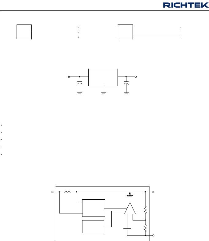
Typical Application Circuit
|
|
|
RT9161/A |
|
VIN |
CIN |
+ |
VIN |
VOUT |
|
|
|
GND |
|
|
1uF |
|
|
|
3  VOUT 2
  VIN
VIN
1  GND
GND
TO-92 (T-Type)
+ |
VOUT |
COUT |
|
10uF |
|
Electrolytic
Functional Pin Description
Pin Name |
Pin Function |
VOUT |
Output Voltage. |
|
|
GND |
Ground. |
VIN |
Power Input. |
|
|
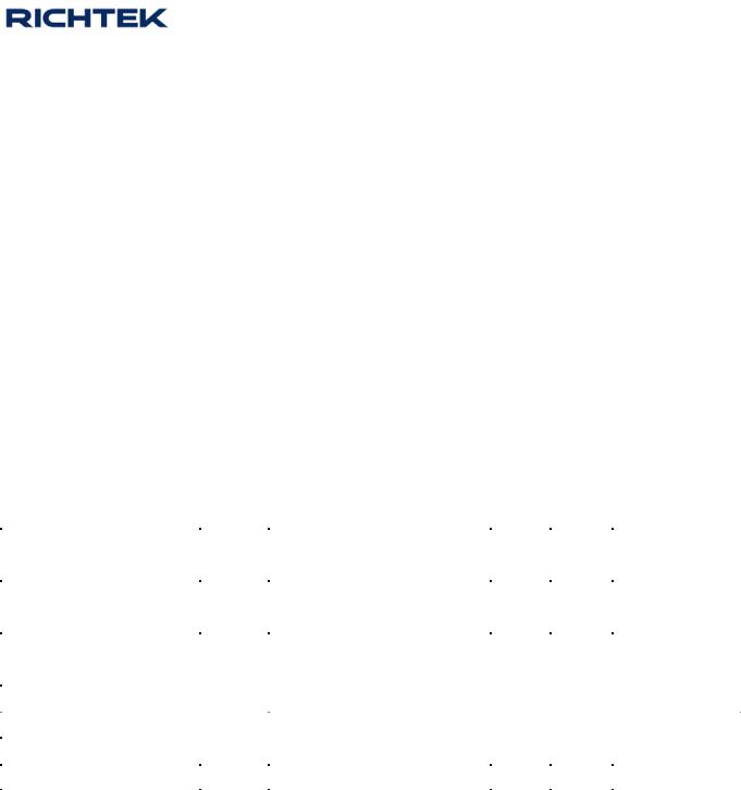
Function Block Diagram
VIN |
|
VOUT |
Current |
Error Amp |
|
Limiting |
- |
+ |
Sensor |
||
Thermal |
1.2V |
|
Shutdown |
|
|
Reference |
|
|
|
GND |
|
|
|
www.richtek.com |
DS9161/A-35 April 2011 |
2
|
|
|
|
|
|
RT9161/A |
||
Absolute Maximum Ratings |
|
|
|
|
||||
z Input Voltage ---------------------------------------------------------------------------------------------------------------- |
|
|
|
|
|
−0.3 to 14V |
||
z Operating Junction Temperature Range ------------------------------------------------------------------------------- |
|
|
|
−40°C to 125°C |
||||
z Storage Temperature Range --------------------------------------------------------------------------------------------- |
|
|
|
|
−65°C to 150°C |
|||
z Power Dissipation, PD @ TA = 25°C |
|
|
|
|
|
|||
SOT-23-3--------------------------------------------------------------------------------------------------------------------- |
|
|
|
|
|
0.4W |
|
|
SOT-89 ----------------------------------------------------------------------------------------------------------------------- |
|
|
|
|
|
0.571W |
||
SOT-223 --------------------------------------------------------------------------------------------------------------------- |
|
|
|
|
|
0.741W |
||
TO-92 ------------------------------------------------------------------------------------------------------------------------- |
|
|
|
|
|
0.625W |
||
z Package Thermal Resistance |
(Note 1) |
|
|
|
|
|
||
SOT-23-3, θJA --------------------------------------------------------------------------------------------------------------- |
|
|
|
|
|
250°C/W |
||
SOT-23-3, θJC --------------------------------------------------------------------------------------------------------------- |
|
|
|
|
|
140°C/W |
||
SOT-89, θJA ----------------------------------------------------------------------------------------------------------------- |
|
|
|
|
|
175°C/W |
||
SOT-89, θJC ----------------------------------------------------------------------------------------------------------------- |
|
|
|
|
|
100°C/W |
||
SOT-223, θJA ---------------------------------------------------------------------------------------------------------------- |
|
|
|
|
|
135°C/W |
||
SOT-223, θJC --------------------------------------------------------------------------------------------------------------- |
|
|
|
|
|
15°C/W |
||
TO-92, θJA ------------------------------------------------------------------------------------------------------------------- |
|
|
|
|
|
160°C/W |
||
TO-92, θJC ------------------------------------------------------------------------------------------------------------------- |
|
|
|
|
|
125°C/W |
||
Electrical Characteristics |
|
|
|
|
|
|||
(TA = 25°C, CIN = 1μF, COUT = 10μF, unless otherwise specified.) |
|
|
|
|
||||
|
|
|
|
|
|
|
|
|
Parameter |
|
Symbol |
Test Conditions |
Min |
Typ |
Max |
Unit |
|
|
|
|
|
|
|
|
|
|
Output Voltage Accuracy |
VOUT |
IL = 1mA, VIN = 5V |
−2 |
-- |
2 |
% |
||
Output Voltage Temperature |
|
|
-- |
50 |
150 |
PPM/°C |
||
Coefficient |
|
|
|
|||||
|
|
|
|
|
|
|
||
|
|
|
|
|
|
|
|
|
Line Regulation |
|
VLINE |
IL = 1mA, VIN= 4.5 to 12V |
-- |
2 |
3 |
%VOUT |
|
Load Regulation |
(Note 2) |
VLOAD |
IL = 1mA to 300/500mA, VIN = 5V |
-- |
1 |
30/50 |
mV |
|
Current Limit |
|
RT9161 |
ILIM |
VIN = 5V, VOUT = 0V |
350 |
580 |
-- |
mA |
(Note 3) |
|
RT9161A |
500 |
900 |
-- |
|||
|
|
|||||||
|
|
|
|
|
|
|
|
|
Dropout Voltage |
(Note 4) |
VDROP |
IL = 300/500mA |
-- |
450/750 |
600/1000 |
mV |
|
|
|
|
|
|
|
|
|
|
Standby Current |
|
ISTANDBY |
IL = 0, VIN = 12V |
-- |
110 |
180 |
μ |
|
|
|
|
|
|
|
A |
||
Note 1. θJA is measured in the natural convection at TA = 25°C on a low effective single layer thermal conductivity test board of JEDEC 51-3 thermal measurement standard.
Note 2. Regulation is measured at constant junction temperature, using pulsed ON time. Note 3. Current Limit is measured at constant junction temperature, using pulsed ON time.
Note 4. The dropout voltage is defined as VIN − VOUT, which is measured when VOUT is VOUT(NORMAL) − 100mV.
DS9161/A-35 April 2011 |
www.richtek.com |
|
3 |

RT9161/A
Typical Operating Characteristics
Output Voltage (V)
Temperature Stability
3.4
3.2 |
|
VOUT = 3.3V |
|
3
2.8
2.6 |
|
|
|
|
|
|
|
|
|
|
|
|
|
|
|
|
|
|
|
VOUT = 2.5V |
|
|
|||
|
|
|
|
|
|
|
|
|
||||
2.4 |
|
|
|
|
|
|
|
|
|
|
|
|
|
|
|
|
|
|
|
|
|
|
|
|
|
|
|
|
|
|
|
|
|
|
|
|
|
|
-50 |
-25 |
0 |
25 |
50 |
75 |
100 |
125 |
|||||
Temperature (°C)
Quiescient Current vs. Temperature
|
0.14 |
|
|
|
|
|
(mA) |
0.12 |
|
|
|
|
|
0.10 |
|
|
|
|
|
|
Current |
0.08 |
|
|
|
|
|
0.06 |
|
|
|
|
|
|
Quiescient |
|
|
|
|
|
|
0.04 |
|
|
|
|
|
|
0.02 |
|
|
|
|
|
|
|
|
|
|
|
|
|
|
|
|
|
|
|
VIN = 5V |
|
0.00 |
|
|
|
|
|
|
-30 |
0 |
30 |
60 |
90 |
120 |
Temperature (°C)
Dropout Voltage (VIN-VOUT)
|
1 |
|
|
|
|
1.4 |
|
|
|
|
|
125°C |
1.2 |
|
0.8 |
|
|
|
|
|
Dropout Voltage (V) |
|
|
|
|
|
|
|
|
|
|
25°C |
1 |
|
0.6 |
|
|
|
|
||
|
|
|
|
0.8 |
||
|
|
|
|
|
||
0.4 |
|
|
|
|
0.6 |
|
|
|
|
|
|
||
|
|
|
|
|
0.4 |
|
0.2 |
|
|
|
|
CurrentCircuitShort(A) |
|
|
|
|
|
|
|
0.2 |
|
0 |
|
|
|
VOUT = 3.3V |
|
|
|
|
|
|
0 |
|
|
0 |
100 |
200 |
300 |
400 |
500 |
ILoad (mA)
Short Circuit Current
|
|
|
125°C |
|
|
|
|
|
25°C |
|
|
0 |
2 |
4 |
6 |
8 |
10 |
Input/Output Differential (V)
Line Transient Response |
Line Transient Response |
Input Voltage |
Deviation (V) |
7 |
COUT = 10μF Electrolytic |
VOUT = 3.3V |
Input Voltage |
Deviation (V) |
7 |
COUT = 10μF Electrolytic |
VOUT = 2.5V |
|
|
|
|||||||||
6 |
IOUT = 0.1A |
|
TA = 25°C |
6 |
IOUT = 0.1A |
TA = 25°C |
||||
5 |
|
T |
|
5 |
T |
|
||||
4 |
|
|
|
4 |
|
|
||||
|
|
|
|
|
|
|
|
|
||
|
|
≈ |
|
T |
|
≈ |
|
≈ |
|
≈ |
Output Voltage |
Deviation (mV) |
100 |
|
|
|
Output Voltage |
Deviation (mV) |
100 |
T |
|
|
|
|
|
|
||||||
2 > |
|
|
|
2 > |
|
|
||||
0 |
|
|
|
0 |
|
|
||||
1 > |
|
|
|
1 > |
|
|
||||
-100 |
|
|
|
-100 |
|
|
||||
|
|
|
|
|
|
|
||||
|
|
-200 |
|
Time 100μS/Div) |
|
|
-200 |
100μS/Div) |
||
|
|
|
|
|
|
|
||||
|
|
|
|
Time (100μs/Div) |
|
|
|
|
Time(100μs/Div) |
|
www.richtek.com |
|
|
|
|
|
DS9161/A-35 April 2011 |
||||
4 |
|
|
|
|
|
|
|
|
|
|
 Loading...