Richtek RT9018A-10GQW, RT9018A-12GQW, RT9018A-12PQW, RT9018A-15GQW, RT9018A-18GQW Schematic [ru]
...
®
RT9018A/B
Maximum 3A, Ultra Low Dropout Regulator
General Description
The RT9018A/B is a high performance positive voltage regulator designed for use in applications requiring very low Input voltage and very low dropout voltage at up to 3A(Peak). It operates with a VIN as low as 1.4V and VDD voltage 3V with output voltage programmable as low as 0.8V. The significant feature includes ultra low dropout, ideal for applications where VOUT is very close to VIN. Additionally, there is an enable pin to further reduce power dissipation while shutdown. The RT9018A/B provides excellent regulation over variations in line, load and temperature. and provides a power OK signal to indicate if the voltage level of Vo reaches 90% of its rating value.
The RT9018A/B is available in the SOP-8 (Exposed Pad) and WDFN-10L 3x3 packages with 1V, 1.05V, 1.2V, 1.5V, 1.8V and 2.5V internally preset outputs that are also adjustable using external resistors.
Features
zMaximum 3A Low-Dropout Voltage Regulator
zHigh Accuracy Output Voltage ±1.5%
zTypically 210mV Dropout at 3A
zPower Good Output
zOutput Voltage Pull Low Resistance when Disable
zThermal and Over Current Protection
zRoHS Compliant and 100% Lead (Pb)-Free
Applications
zFront Side Bus VTT (1.2V/3A)
zNoteBook PC Applications
zMotherboard Applications
Marking Information
For marking information, contact our sales representative directly or through a Richtek distributor located in your area.
Ordering Information
RT9018A/B-


Package Type
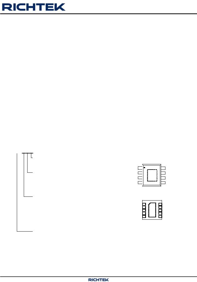
SP : SOP-8 (Exposed Pad-Option 1) QW : WDFN-10L 3x3
Lead Plating System P : Pb Free
G : Green (Halogen Free and Pb Free) Z : ECO (Ecological Element with
Halogen Free and Pb free)
Output Voltage 10 : 1V/Adj 1K : 1.05V/Adj 12 : 1.2V/Adj 15 : 1.5V/Adj 18 : 1.8V/Adj 25 : 2.5V/Adj
Enable Pin Function
A : Internal Pull High
B : Internal Pull Low
Note :
Richtek products are :
`RoHS compliant and compatible with the current requirements of IPC/JEDEC J-STD-020.
`Suitable for use in SnPb or Pb-free soldering processes.
Pin Configurations
(TOP VIEW)
PGOOD |
|
|
8 |
GND |
EN |
2 |
GND |
7 |
ADJ |
VIN |
3 |
9 |
6 |
VOUT |
VDD |
4 |
|
5 |
NC |
SOP-8 (Exposed Pad)
VOUT 1 |
|
10 |
VDD |
|
VOUT 2 |
|
9 |
VIN |
|
VOUT 3 |
GND |
8 |
VIN |
|
ADJ |
4 |
|
7 |
VIN |
PGOOD |
5 |
11 |
9 |
EN |
WDFN-10L 3x3
Copyright ©2012 Richtek Technology Corporation. All rights reserved. |
is a registered trademark of Richtek Technology Corporation. |
DS9018A/B-09 April 2012 |
www.richtek.com |
|
1 |

RT9018A/B
Typical Application Circuit
VIN |
|
VIN |
VOUT |
VOUT |
|
10µF |
RT9018A/B |
10µF |
|
|
|
|||
Chip Enable |
|
EN |
ADJ |
|
|
|
|
||
VDD |
|
VDD |
PGOOD |
|
|
|
|
GND |
100k |
|
1µF |
|
|
|
|
|
|
|
VOUT |
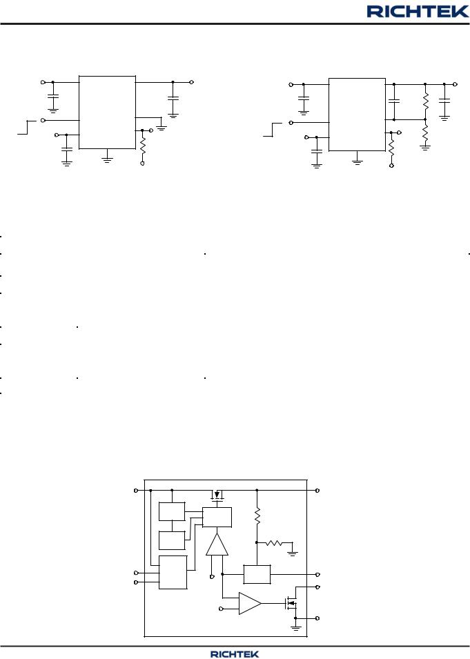
Figure 1. Fixed Voltage Regulator
|
|
|
VOUT =0.8 ×R1+R2 |
|
|
|
|
|
R2 |
VIN |
VIN |
VOUT |
CDummy |
VOUT |
10µF |
RT9018A/B |
R1 |
||
|
10µF |
|||
Chip Enable |
EN |
ADJ |
|
|
|
|
R2 |
||
VDD |
VDD |
PGOOD |
|
|
|
|
|||
|
|
GND |
100k |
|
1µF |
|
|
|
|
|
|
VOUT |
|
|
Figure 2. Adjustable Voltage Regulator
Function Pin Description
Pin No. |
Pin |
Pin Function |
|
|
|
||
SOP-8 |
WDFN-10L 3x3 |
Name |
|
(Exposed Pad) |
|
|
|
|
|
|
|
3 |
7, 8, 9 |
VIN |
Supply Input Voltage. |
|
|
|
|
2 |
6 |
EN |
Chip Enable (Active-High). |
|
|
|
|
4 |
10 |
VDD |
Supply Voltage of Control Circuitry. |
|
|
|
|
1 |
5 |
PGOOD |
Power Good Open Drain Output. |
|
|
|
|
|
|
|
Set the output voltage by the internal feedback resistors when |
7 |
4 |
ADJ |
ADJ is grounded. If external feedback resistors is used, VOUT = |
|
|
|
0.8V x (R1 + R2)/R2. |
6 |
1, 2, 3 |
VOUT |
Output Voltage. |
|
|
|
|
5 |
-- |
NC |
No Internal Connection. |
|
|
|
|
8, |
11 (Exposed Pad) |
GND |
Ground. The exposed pad must be soldered to a large PCB |
9 (Exposed Pad) |
and connected to GND for maximum power dissipation. |
||
Function Block Diagram
VIN |
|
|
|
VOUT |
|
OCP |
Driver |
|
|
|
|
|
|
|
|
OTP |
|
Error |
|
|
+ - |
Amplifier |
|
|
|
|
|
|
|
EN |
POR |
|
Mode |
ADJ |
VDD |
|
0.8V |
|
PGOOD |
|
|
|
- |
|
|
|
|
|
|
|
|
0.72V |
+ |
GND |
|
|
|
|
Copyright ©2012 Richtek Technology Corporation. All rights reserved. |
is a registered trademark of Richtek Technology Corporation. |
|
|
www.richtek.com |
DS9018A/B-09 April 2012 |
2

|
|
|
|
|
|
|
RT9018A/B |
|||||
Absolute Maximum Ratings (Note 1) |
|
|
|
|
|
|
|
|
||||
z Supply Voltage, VIN ------------------------------------------------------------------------------------------------------ |
|
|
|
|
|
|
|
1V to 6V |
|
|||
z Control Voltage, VDD ----------------------------------------------------------------------------------------------------- |
|
|
|
|
|
|
|
3V to 6V |
|
|||
z Output Voltage, VOUT --------------------------------------------------------------------------------------------------- |
|
|
|
|
|
|
|
0.8 to 6V |
|
|||
z Power Dissipation, PD @ TA = 25°C |
|
|
|
|
|
|
|
|
|
|
||
|
SOP-8 (Exposed Pad) --------------------------------------------------------------------------------------------------- |
|
|
|
|
|
|
|
1.33W |
|
||
|
WDFN-10L 3x3 ------------------------------------------------------------------------------------------------------------- |
|
|
|
|
|
|
|
|
1.67W |
|
|
z Package Thermal Resistance (Note 2) |
|
|
|
|
|
|
|
|
||||
|
SOP-8 (Exposed Pad), θJA ---------------------------------------------------------------------------------------------- |
|
|
|
|
|
|
|
75°C/W |
|
||
|
SOP-8 (Exposed Pad), θJC --------------------------------------------------------------------------------------------- |
|
|
|
|
|
|
|
15°C/W |
|
||
|
WDFN-10L 3x3, θJA ------------------------------------------------------------------------------------------------------- |
|
|
|
|
|
|
|
60°C/W |
|
||
z Junction Temperature ----------------------------------------------------------------------------------------------------- |
|
|
|
|
|
|
|
150°C |
|
|||
z Lead Temperature (Soldering, 10 sec.) |
------------------------------------------------------------------------------- |
|
|
|
|
|
|
260°C |
|
|||
z Storage Temperature Range -------------------------------------------------------------------------------------------- |
|
|
|
|
|
|
|
−65°C to 150°C |
||||
z ESD Susceptibility |
(Note 3) |
|
|
|
|
|
|
|
|
|
|
|
|
HBM (Human Body Mode) ---------------------------------------------------------------------------------------------- |
|
|
|
|
|
|
|
2kV |
|
||
|
MM (Machine Mode) ------------------------------------------------------------------------------------------------------ |
|
|
|
|
|
|
|
200V |
|
||
Recommended Operating Conditions (Note 4) |
|
|
|
|
|
|
||||||
z Supply Voltage, VIN ------------------------------------------------------------------------------------------------------- |
|
|
|
|
|
|
|
1.4V to 5.5V |
||||
z Control Voltage, VDD (VDD > VOUT + 1.5V) -------------------------------------------------------------------------- |
|
|
|
|
|
3V to 5.5V |
||||||
z Control Voltage with PGOOD, VDD (Note 8) ----------------------------------------------------------------------- |
|
|
|
|
|
4.5V to 5.5V |
||||||
z Junction Temperature Range -------------------------------------------------------------------------------------------- |
|
|
|
|
|
|
|
−40°C to 125°C |
||||
z Ambient Temperature Range -------------------------------------------------------------------------------------------- |
|
|
|
|
|
|
|
−40°C to 85°C |
||||
Electrical Characteristics |
|
|
|
|
|
|
|
|
|
|
||
(VIN = VOUT + 500mV, VEN = VDD = 5V, CIN = COUT = 10μF, TA = TJ = 25°C, unless otherwise specified) |
|
|
|
|
||||||||
|
Parameter |
Symbol |
|
Test Conditions |
Min |
|
Typ |
Max |
|
Unit |
||
|
|
|
|
|
|
|
|
|
|
|
|
|
|
POR Threshold |
|
|
|
|
|
2.4 |
|
2.7 |
3 |
|
V |
|
|
|
|
|
|
|
|
|
|
|
|
|
|
POR Hysteresis |
|
|
|
|
|
0.15 |
|
0.2 |
-- |
|
V |
|
|
|
|
|
|
|
|
|
|
|
|
|
|
Adjustable Pin Threshold |
VTH_ADJ |
|
IOUT = 1mA |
|
-- |
|
0.2 |
0.4 |
|
V |
|
|
Reference Voltage (ADJ Pin Voltage) |
VADJ |
|
IOUT = 1mA |
|
0.788 |
|
0.8 |
0.812 |
|
V |
|
|
Fixed Output Voltage Range |
VOUT |
|
|
|
−1.5 |
|
0 |
1.5 |
|
% |
|
|
Line Regulation (VIN) |
VLINE_IN |
|
VIN = VOUT |
+ 0.5V to 5V, |
-- |
|
0.2 |
0.6 |
|
% |
|
|
|
IOUT = 1mA |
|
|
|
|||||||
|
|
|
|
|
|
|
|
|
|
|
|
|
|
Load Regulation |
(Note 5) |
VLOAD |
|
VIN = VOUT |
+ 1V, |
-- |
|
0.2 |
1 |
|
% |
|
|
IOUT = 1mA to 3A |
|
|
||||||||
|
|
|
|
|
|
|
|
|
|
|
||
|
Dropout Voltage (Note 6) |
VDROP |
|
IOUT = 2A |
|
-- |
|
150 |
250 |
|
mV |
|
|
|
IOUT = 3A |
|
-- |
|
210 |
350 |
|
||||
|
|
|
|
|
|
|
|
|
||||
|
Quiescent Current (Note 7) |
IQ |
|
VDD = 5.5V |
|
-- |
|
0.6 |
1.2 |
|
mA |
|
|
Current Limit |
|
ILIM |
|
|
|
3.2 |
|
4.5 |
-- |
|
A |
|
|
|
|
|
|
|
|
|
|
|
|
|
Copyright ©2012 Richtek Technology Corporation. All rights reserved. |
|
is a registered trademark of Richtek Technology Corporation. |
|
|||||||||
DS9018A/B-09 April |
2012 |
|
|
|
|
|
|
|
www.richtek.com |
|||
|
|
|
|
|
|
|
|
|
|
|
|
3 |

RT9018A/B
Parameter |
|
Symbol |
Test Conditions |
Min |
Typ |
Max |
Unit |
|
Short Circuit Current |
|
|
VOUT < 0.2V |
0.5 |
1.8 |
-- |
A |
|
In-rush Current |
|
|
μ |
-- |
0.6 |
-- |
A |
|
|
|
|
|
COUT = 10 F, Enable Start-up |
||||
VOUT Pull Low Resistance |
|
VEN = 0V |
-- |
150 |
-- |
Ω |
||
Chip Enable |
|
|
|
|
|
|
|
|
EN Input Bias Current |
|
IEN |
VEN = 0V |
-- |
12 |
-- |
μA |
|
VDD Shutdown |
|
RT9018A |
ISHDN |
VEN = 0V |
-- |
10 |
20 |
μA |
Current |
|
RT9018B |
-- |
-- |
1 |
|||
|
|
|
|
|||||
EN Threshold Voltage |
|
Logic-Low |
VENL |
VDD = 5V |
-- |
-- |
0.7 |
V |
|
Logic-High |
VENH |
VDD = 5V |
1.2 |
-- |
-- |
||
|
|
|
||||||
Power Good |
|
|
|
|
|
|
|
|
PGOOD Rising Threshold |
|
|
-- |
90 |
93 |
% |
||
PGOOD Hysteresis |
|
|
|
3 |
10 |
-- |
% |
|
PGOOD Sink Capability |
|
IPGOOD = 10mA |
-- |
0.2 |
0.4 |
V |
||
PGOOD Delay |
|
|
|
0.5 |
1.5 |
5 |
ms |
|
Thermal Protection |
|
|
|
|
|
|
|
|
Thermal Shutdown Temperature |
TSD |
|
-- |
160 |
-- |
°C |
||
Thermal Shutdown Hysteresis |
TSD |
|
-- |
30 |
-- |
°C |
||
Thermal Shutdown Temperature |
|
VOUT < 0.4V |
-- |
110 |
-- |
°C |
||
Fold-back |
|
|
||||||
|
|
|
|
|
|
|
||
Note 1. Stresses beyond those listed “Absolute Maximum Ratings” may cause permanent damage to the device. These are stress ratings only, and functional operation of the device at these or any other conditions beyond those indicated in the operational sections of the specifications is not implied. Exposure to absolute maximum rating conditions may affect device reliability.
Note 2. θJA is measured at TA = 25°C on a high effective thermal conductivity four-layer test board per JEDEC 51-7. θJC is measured at the exposed pad of the package.
Note 3. Devices are ESD sensitive. Handling precaution recommended.
Note 4. The device is not guaranteed to function outside its operating conditions.
Note 5. Regulation is measured at constant junction temperature by using a 2ms current pulse. Devices are tested for load regulation in the load range from 1mA to 3A.
Note 6. The dropout voltage is defined as VIN -VOUT, which is measured when VOUT is VOUT(NORMAL) - 100mV.
Note 7. Quiescent, or ground current, is the difference between input and output currents. It is defined by IQ = IIN - IOUT under no load condition (IOUT = 0mA). The total current drawn from the supply is the sum of the load current plus the ground pin current.
Note 8. The control voltage must within 4.5V to 5.5V when using PGOOD function.
Copyright ©2012 Richtek Technology Corporation. All rights reserved. |
is a registered trademark of Richtek Technology Corporation. |
|
|
www.richtek.com |
DS9018A/B-09 April 2012 |
4 |
|
 Loading...