


RT9013B-12GU5
Richtek RT9013B-12GU5, RT9013B-15PQWA, RT9013B-15PU5, RT9013B-18PQWA, RT9013B-18PU5 Schematic [ru]
...
RT9013B
300mA, Low Dropout, Low Noise Ultra-Fast Without
Bypass Capacitor CMOS LDO Regulator
General Description
The RT9013B is a high-performance, 300mA LDO regulator,
offering extremely high PSRR and ultra-low dropout. The
RT9013B is Ideal for portable RF and wireless applications
with demanding performance and space requirements.
The RT9013B provides quiescent current to be as low as
25uA to extend the battery life. The RT9013B also works
with low-ESR ceramic capacitors, reducing the amount of
board space necessary for power applications, especially
for hand-held wireless devices.
The RT9013B consumes typical 0.7uA in shutdown mode
and has fast turn-on time to be less than 40us. The other
features include ultra-low dropout voltage, high output
accuracy, current limiting protection, and high ripple
rejection ratio. The RT9013B is available in the SC-70-5
and WDFN-6L 1.6x1.6 packages.
Ordering Information
RT9013B
-
Package Type
U5 : SC-70-5
QWC : WDFN-6L 1.6x1.6 (W-Type)
Lead Plating System
P : Pb Free
G : Green (Halogen Free and Pb Free)
Features
Wide Operating Voltage Range : 2.2V to 5.5V
Low Dropout : 150mV at 300mA
Ultra-Low-Noise for RF Application
Ultra-Fast in Line/Load Transient Response
Current Limiting Protection
Thermal Shutdown Protection
High Power Supply Rejection Ratio
Only 1uF Output Capacitor Required for Stability
TTL-Logic-Controlled Shutdown Input
RoHS Compliant and 100% Lead (Pb)-Free
Applications
CDMA/GSM Cellular Handsets
Portable Information Appliances
Laptop, Palmtops, Notebook Computers
Hand-Held Instruments
Mini PCI & PCI-Express Cards
PCMCIA & New Cards
Marking Information
For marking information, contact our sales representative
directly or through a Richtek distributor located in your
area.
Fixed Output Voltage
12 : 1.2V
13 : 1.3V
:
34 : 3.4V
35 : 3.5V
1B : 1.25V
1H : 1.85V
2H : 2.85V
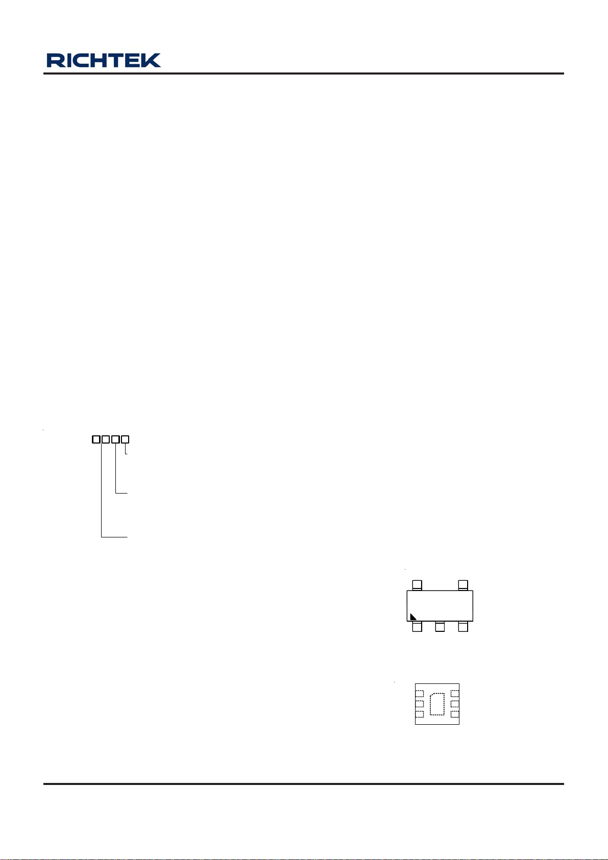
Pin Configurations
(TOP VIEW)
VOUT
54
23
GND
VIN EN
NC
Note :
EN
VIN
SC-70-5
1
2
GND
7
3
6
5
4
NC
NCGND
VOUT
Richtek products are :
` RoHS compliant and compatible with the current require-
ments of IPC/JEDEC J-STD-020.
` Suitable for use in SnPb or Pb-free soldering processes.
WDFN-6L 1.6x1.6
DS9013B-02 April 2011 www.richtek.com
1
RT9013B
Typical Application Circuit
V
IN
1uF/X7R
Chip Enable
C
IN
R
pull_down
100k
VIN
RT9013B
EN
GND
Functional Pin Description
Pin No.
SC-70-5 WDFN-6L 1.6x1.6
1 3 VIN Supply Input.
2
7 (Exposed Pad)
2,
3 1 EN
4 5, 6 NC No Internal Connection.
5 4 VOUT Regulator Output.
Pin Name
GND
Common Ground. The exposed pad must be soldered to a large PCB
and connected to GND for maximum power dissipation.
Chip Enable (Active High). It is recommended to add a 100kΩ resistor
between the EN and GND.
VOUT
NC
V
OUT
C
OUT
1uF/X7R
Pin Function
Function Block Diagram
EN
POR
OTP
Current
Limit
VIN
V
REF
+
MOS
Driver
VOUT
GND
DS9013B-02 April 2011www.richtek.com
2
RT9013B
Absolute Maximum Ratings (Note 1)
Supply Input Voltage ------------------------------------------------------------------------------------------------------ 6V
EN Input Voltage ----------------------------------------------------------------------------------------------------------- 6V
Power Dissipation, P
SC-70-5 ---------------------------------------------------------------------------------------------------------------------- 0.3W
WDFN-6L 1.6x1.6 --------------------------------------------------------------------------------------------------------- 0.606W
Package Thermal Resistance (Note 2)
SC-70-5, θJA---------------------------------------------------------------------------------------------------------------- 333°C/W
WDFN-6L 1.6x1.6, θJA---------------------------------------------------------------------------------------------------- 165°C/W
Lead Temperature (Soldering, 10 sec.)------------------------------------------------------------------------------- 260°C
Junction Temperature ----------------------------------------------------------------------------------------------------- 150°C
Storage Temperature Range -------------------------------------------------------------------------------------------- −65°C to 150°C
ESD Susceptibility (Note 3)
HBM -------------------------------------------------------------------------------------------------------------------------- 2kV
MM ---------------------------------------------------------------------------------------------------------------------------- 200V
Recommended Operating Conditions (Note 4)
Supply Input Voltage ------------------------------------------------------------------------------------------------------ 2.2V to 5.5V
Junction Temperature Range --------------------------------------------------------------------------------------------
Ambient Temperature Range --------------------------------------------------------------------------------------------
@ T
D
= 25°C
A
−40°C to 125°C
−40°C to 85°C
Electrical Characteristics
(V
= V
+ 0.5V, V
OUT
IN
Parameter Symbol Test Conditions Min Typ Max Unit
Input Voltage Range VIN 2.2 -- 5.5 V
Output Noise Voltage VON V
Ou tput V oltage Acc ur acy
(Fixed Output Voltage)
Quiescent Current (Note 5) IQ V
Shutdown Current I
Current Limit I
Dropout Voltage (Note 6) V
Load Regulation (Note 7)
(Fixed Output Voltage)
EN Threshold
Enable Pin Current IEN -- 0.1 1 uA
Power Supply Rejection Rate PSRR I
Line Regulation ΔV
Thermal Shutdown Temperature TSD -- 170 --
Thermal Shutdown Hysteresis ΔTSD -- 30 --
= VIN, C
EN
= C
IN
OUT
Logic-Low Voltage V
Logic-High Voltage V
= 1uF/X7R (Ceramic), T
= 1.5V -- 30 -- uV
OU T
ΔV
I
OUT
VEN = 0V -- 0.7 1.5 uA
SHDN
R
LIM
I
DROP
= 10mA −2 0 +2 %
OUT
= 5V, I
EN
LOAD
= 300mA -- 125 240 mV
OUT
1mA < I
ΔV
LOA D
2.2V ≤ V
1mA < I
2.7V ≤ V
0 -- 0.6
IL
1.6 -- 5.5
IH
= 100mA, f = 10kHz -- −50 -- dB
OUT
V
= (V
IN
LINE
I
OUT
= 1mA
= 25°C, unless otherwise specified)
A
= 0mA -- 25 50 uA
OUT
= 0Ω, 2.2V ≤ VIN < 5.5V 300 400 600 mA
< 300mA
OUT
< 2.7V
IN
< 300mA
OUT
≤ 5.5V
IN
+ 0.5) to 5.5V,
OU T
-- -- 0.6
-- -- 1
-- 0.01 0.2 %/V
RMS
%
V
°C
DS9013B-02 April 2011 www.richtek.com
3

RT9013B
Note 1. Stresses listed as the above “Absolute Maximum Ratings” may cause permanent damage to the device. These are for
stress ratings. Functional operation of the device at these or any other conditions beyond those indicated in the operational
sections of the specifications is not implied. Exposure to absolute maximum rating conditions for extended periods may
remain possibility to affect device reliability.
Note 2. θ
is measured in the natural convection at T
JA
JEDEC 51-3 thermal measurement standard.
Note 3. Devices are ESD sensitive. Handling precaution is recommended.
Note 4. The device is not guaranteed to function outside its operating conditions.
Note 5. Quiescent, or ground current, is the difference between input and output currents. It is defined by I
load condition (I
= 0mA). The total current drawn from the supply is the sum of the load current plus the ground pin
OUT
current.
Note 6. The dropout voltage is defined as V
-V
IN
Note 7. Regulation is measured at constant junction temperature by using a 2ms current pulse. Devices are tested for load
regulation in the load range from 10mA to 300mA.
= 25°C on a low effective thermal conductivity single layer test board of
A
= IIN - I
Q
, which is measured when V
OUT
OUT
is V
OUT(NORMAL)
- 100mV.
under no
OUT
DS9013B-02 April 2011www.richtek.com
4
 Loading...