


Richtek RT9011-BJGJ6, RT9011-BMPJ6, RT9011-BMPQW, RT9011-CBGJ6, RT9011-CCPJ6 Schematic [ru]
...RT9011
Portable Power Management 300mA Dual LDO Regulator
General Description
The RT9011 is a dual channel, low noise, and low dropout regulator sourcing up to 300mAat each channel. The range of output voltage is from 1.2V to 3.6V by operating from 2.5V to 5.5V input.
The RT9011 offers 2% accuracy, extremely low dropout voltage (240mV @ 300mA), and extremely low ground current, only 27μA per LDO. The shutdown current is near zero current which is suitable for battery-power devices. Other features include current limiting, over temperature, output short circuit protection.
The RT9011 is short circuit thermal folded back protected. The IC lowers its OTP trip point from 165°C to 110°C when output short circuit occurs (VOUT < 0.4V) providing maximum safety to end users.
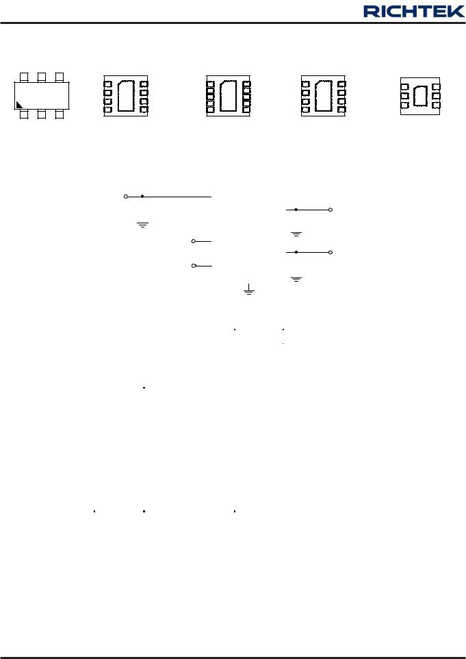
The RT9011 can operate stably with very small ceramic output capacitors, reducing required board space and component cost. The RT9011 is available in fixed output voltages in the TSOT-23-6, WDFN-8L 2x2, WDFN-10L 3x3, WDFN-8L 3x3 and WDFN-6L 1.6x1.6 packages.
Ordering Information
RT9011-


Package Type
J6 : TSOT-23-6
QW : WDFN-8L 2x2 (W-Type)
QWA : WDFN-10L 3x3 (W-Type)
QWB : WDFN-8L 3x3 (W-Type)
QWC : WDFN-6L 1.6x1.6 (W-Type)
Lead Plating System
P : Pb Free
G : Green (Halogen Free and Pb Free)
Output Voltage : VOUT1/VOUT2
VOUT2 > VOUT1 is Recommended
Note :
Richtek products are :
`RoHS compliant and compatible with the current requirements of IPC/JEDEC J-STD-020.
`Suitable for use in SnPb or Pb-free soldering processes.
Features
zWide Operating Voltage Ranges : 2.5V to 5.5V
zLow-Noise for RF Application
zNo Noise Bypass Capacitor Required
zFast Response in Line/Load Transient
zTTL-Logic-Controlled Shutdown Input
zLow Temperature Coefficient
zDual LDO Outputs (300mA/300mA)
zUltra-low Quiescent Current 27μA/LDO
zHigh Output Accuracy 2%
zShort Circuit Protection
zThermal Shutdown Protection
zCurrent Limit Protection
zShort Circuit Thermal Folded Back Protection
zTiny TSOT-23-6 and 6-Lead/8-Lead/10-Lead WDFN Packages
zRoHS Compliant and 100% Lead (Pb)-Free
Applications
zCDMA/GSM Cellular Handsets
zBattery-Powered Equipment
zLaptop, Palmtops, Notebook Computers
zHand-Held Instruments
zPCMCIA Cards
zPortable Information Appliances
Marking Information
For marking information, contact our sales representative directly or through a Richtek distributor located in your area.
Available Voltage Version
Code |
Voltage |
Code |
Voltage |
Code |
Voltage |
A |
3.5 |
B |
1.3 |
C |
1.2 |
D |
1.85 |
E |
2.1 |
F |
1.5 |
G |
1.8 |
H |
2 |
J |
2.5 |
K |
2.6 |
L |
2.7 |
M |
2.8 |
N |
2.85 |
P |
3 |
Q |
3.1 |
R |
3.2 |
S |
3.3 |
T |
2.65 |
V |
2.9 |
W |
1.6 |
X |
3.15 |
Y |
1.9 |
|
|
|
|
DS9011-08 April 2011 |
www.richtek.com |
|
1 |
RT9011
Pin Configurations
VOUT1 VIN EN1
6 5 |
4 |
VIN 1 |
8 |
VOUT1 |
|
|
|
EN1 2 |
7 |
VOUT2 |
|
|
|
EN2 3 |
GND |
NC |
|
2 |
3 |
6 |
|||
NC 4 |
9 5 |
GND |
|||
|
|
||||
VOUT2 GND EN2 |
|
|
|
||
TSOT-23-6 |
WDFN-8L 2x2 |
||||
(TOP VIEW)
VIN 1 |
|
10 |
VOUT1 |
VIN 1 |
|
8 |
VOUT1 |
VIN |
1 |
|
6 |
VOUT1 |
||
EN1 2 |
|
9 |
VOUT2 |
EN1 |
2 |
|
7 |
NC |
|
|||||
GND |
GND |
EN1 |
2 |
GND |
5 |
VOUT2 |
||||||||
EN2 3 |
8 |
NC |
EN2 |
3 |
6 |
GND |
||||||||
NC 4 |
11 |
7 |
NC |
9 |
EN2 3 |
7 |
4 |
GND |
||||||
NC 5 |
9 |
GND |
NC 4 |
5 |
VOUT2 |
|
|
|
|
|
||||
WDFN-10L 3x3 |
WDFN-8L 3x3 |
WDFN-6L 1.6x1.6 |
||||||||||||
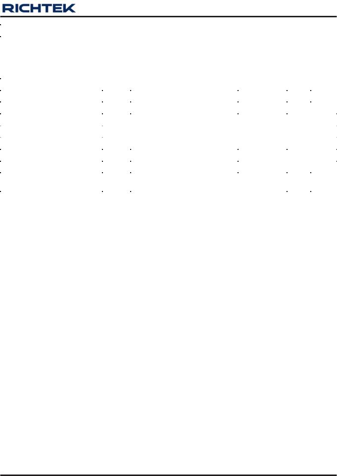
Typical Application Circuit
VIN |
|
|
VIN |
|
|
|
VOUT1 |
|||||
|
|
|
|
|||||||||
|
|
|
|
CIN |
VOUT1 |
|
|
|
||||
|
|
|
|
|
|
|
||||||
|
|
|
|
|
|
|
||||||
|
|
|
|
1uF |
|
|
|
|
COUT1 |
|||
|
|
|
|
|||||||||
|
|
|
|
|
|
|
|
RT9011 |
|
|
|
1uF |
|
|
|
|
Chip Enable |
EN1 |
|
|
|
|
|||
|
|
|
|
VOUT2 |
|
|
|
VOUT2 |
||||
|
|
|
|
|
|
|
|
|
|
|
||
|
|
|
|
|
|
|
|
EN2 |
|
|
|
COUT2 |
|
|
|
|
|
|
|
|
|
|
|
||
|
|
|
|
|
|
|
|
|
|
|
1uF |
|
|
|
|
|
|
|
|
|
GND |
|
|
|
|
|
|
|
|
|
|
|
|
|
|
|
|
|
Functional Pin Description
|
|
Pin No. |
|
|
|
|
TSOT-23-6 |
WDFN-8L |
WDFN-10L |
WDFN-8L |
WDFN-6L |
Pin Name |
Pin Function |
|
2x2 |
3x3 |
3x3 |
1.6x1.6 |
|
|
5 |
1 |
1 |
1 |
1 |
VIN |
Supply Input. |
|
|
|
|
|
|
|
4 |
2 |
2 |
2 |
2 |
EN1 |
Chip Enable1 (Active High). |
3 |
3 |
3 |
3 |
3 |
EN2 |
Chip Enable2 (Active High). |
|
|
|
|
|
|
|
|
5, |
6, |
6, |
4, |
|
Common Ground. The exposed pad must be |
2 |
Exposed |
Exposed |
Exposed |
Exposed |
GND |
soldered to a large PCB and connected to |
|
Pad (9) |
Pad (11) |
Pad (9) |
Pad (7) |
|
GND for maximum power dissipation. |
|
|
|
|
|
|
|
1 |
7 |
9 |
5 |
5 |
VOUT2 |
Channel 2 Output Voltage. |
6 |
8 |
10 |
8 |
6 |
VOUT1 |
Channel 1 Output Voltage. |
-- |
4, 6 |
4, 5, 7, 8 |
4, 7 |
-- |
NC |
No Internal Connection. |
|
|
|
|
|
|
|
www.richtek.com |
DS9011-08 April 2011 |
2

RT9011
Function Block Diagram
EN1 |
0.2uA |
Shutdown |
VIN |
|
|||
|
|
and |
|
|
|
Logic Control |
|
|
VREF |
|
|
|
- |
MOS Driver |
|
|
+ |
|
|
|
Error |
VOUT1 |
|
|
Amplifier |
||
|
|
Current-Limit |
|
|
|
and |
|
|
|
Thermal |
|
|
|
Protection |
|
|
|
|
GND |
EN2 |
0.2uA |
Shutdown |
|
|
|
||
|
|
and |
|
|
|
Logic Control |
|
|
VREF |
|
|
|
- |
MOS Driver |
|
|
+ |
|
|
|
Error |
|
|
|
|
VOUT2 |
|
|
Amplifier |
||
|
|
Current-Limit |
|
|
|
and |
|
|
|
Thermal |
|
|
|
Protection |
|
|
|
|
GND |
DS9011-08 April 2011 |
www.richtek.com |
3

RT9011
Absolute Maximum Ratings (Note 1)
z Supply Input Voltage ------------------------------------------------------------------------------------------------------ |
−0.3V to 7V |
z Other I/O Pin Voltages --------------------------------------------------------------------------------------------------- |
−0.3V to 7V |
z Power Dissipation, PD @ TA = 25°C |
|
TSOT-23-6 ------------------------------------------------------------------------------------------------------------------- |
0.455W |
WDFN-8L 2x2 -------------------------------------------------------------------------------------------------------------- |
0.606W |
WDFN-10L 3x3 ------------------------------------------------------------------------------------------------------------- |
0.926W |
WDFN-8L 3x3 -------------------------------------------------------------------------------------------------------------- |
0.926W |
WDFN-6L 1.6x1.6 --------------------------------------------------------------------------------------------------------- |
0.571W |
z Package Thermal Resistance (Note 2) |
|
TSOT-23-6, θJA ------------------------------------------------------------------------------------------------------------- |
220°C/W |
WDFN-8L 2x2, θJA --------------------------------------------------------------------------------------------------------- |
165°C/W |
WDFN-10L 3x3, θJA ------------------------------------------------------------------------------------------------------- |
108°C/W |
WDFN-8L 3x3, θJA --------------------------------------------------------------------------------------------------------- |
108°C/W |
WDFN-6L 1.6x1.6, θJA ---------------------------------------------------------------------------------------------------- |
175°C/W |
z Junction Temperature ----------------------------------------------------------------------------------------------------- |
150°C |
z Lead Temperature (Soldering, 10 sec.) ------------------------------------------------------------------------------- |
260°C |
z Storage Temperature Range -------------------------------------------------------------------------------------------- |
−65°C to 150°C |
z ESD Susceptibility (Note 3) |
|
HBM (Human Body Mode) ---------------------------------------------------------------------------------------------- |
2kV |
MM (Machine Mode) ------------------------------------------------------------------------------------------------------ |
200V |
Recommended Operating Conditions |
(Note 4) |
z Supply Input Voltage ------------------------------------------------------------------------------------------------------ |
2.5V to 5.5V |
z Enable Input Voltage ------------------------------------------------------------------------------------------------------ |
0V to 5.5V |
z Junction Temperature Range -------------------------------------------------------------------------------------------- |
−40°C to 125°C |
z Ambient Temperature Range -------------------------------------------------------------------------------------------- |
−40°C to 85°C |
Electrical Characteristics
(VIN = VOUT + 1V, VEN = VIN, CIN = COUT = 1μF, TA = −40°C to 85°C, unless otherwise specified.)
Parameter |
Symbol |
Test Conditions |
|
Min |
Typ |
Max |
Unit |
|
|
|
|
|
|
|
|
|
|
Input Voltage |
|
VIN = 2.5V to 5.5V |
|
2.5 |
-- |
5.5 |
V |
|
Dropout Voltage (Note 5) |
VDROP |
IOUT = 300mA |
|
-- |
240 |
330 |
mV |
|
Output voltage range |
VOUT |
|
|
1.2 |
-- |
3.6 |
V |
|
VOUT Accuracy |
V |
IOUT = 1mA to 300mA |
|
− |
-- |
+3 |
% |
|
|
3 |
|
|
|
|
|||
Line Regulation |
VLINE |
VIN = (VOUT + 0.3V) to 5.5V |
or |
-- |
-- |
0.2 |
%/V |
|
VIN > 2.5V, whichever is larger |
|
|
||||||
|
|
|
|
|
|
|
||
Load Regulation |
VLOAD |
1mA < IOUT< 300mA |
|
-- |
-- |
0.6 |
% |
|
Current Limit |
|
RLOAD = 1Ω |
|
330 |
450 |
700 |
mA |
|
|
|
|
|
|
|
|
|
|
Quiescent Current |
IQ |
VEN > 1.5V |
|
-- |
58 |
80 |
μA |
|
Shutdown Current |
IQ_SD |
VEN < 0.4V |
|
-- |
-- |
1 |
μ |
|
|
|
|
|
|
A |
|
||
EN Threshold |
VIH |
VIN = 2.5V to 5.5V, Power On |
|
1.5 |
-- |
-- |
V |
|
VIL |
VIN = 2.5V to 5.5V, Shutdown |
|
-- |
-- |
0.4 |
|
||
|
|
|
|
|||||
|
|
|
|
|
|
To be continued |
||
www.richtek.com |
|
|
|
|
DS9011-08 |
April 2011 |
||
4
RT9011
Parameter |
|
Symbol |
Test Conditions |
Min |
Typ |
Max |
Unit |
Output Voltage TC |
|
|
|
-- |
100 |
-- |
ppm/°C |
|
|
|
|
|
|
|
|
VOUT Discharge Resistance |
in |
|
VIN = 5V, EN1 = EN2 = GND |
-- |
3 |
-- |
kΩ |
Shutdown (Note 6) |
|
|
|||||
|
|
|
|
|
|
|
|
EN Pull Low Current |
|
IEN |
|
-- |
0.2 |
-- |
μA |
|
|
|
|
|
|
|
|
Thermal Shutdown |
|
TSD |
|
-- |
170 |
-- |
°C |
Thermal Shutdown Hysteresis |
|
TSD |
|
-- |
40 |
-- |
°C |
|
|
|
f = 100Hz |
-- |
70 |
-- |
|
|
|
|
|
|
|
|
|
PSRR |
|
|
f = 1kHz |
-- |
70 |
-- |
|
|
|
|
|
|
|
|
|
|
|
f = 10kHz |
-- |
70 |
-- |
|
|
VIN = VOUT + 1V, COUT = 2.2μF |
|
PSRR |
dB |
||||
|
|
|
|
|
|||
|
f = 100kHz |
-- |
54 |
-- |
|||
ILOAD = 50mA |
|
|
|
||||
|
|
|
|
|
|
|
|
|
|
|
f = 200kHz |
-- |
45 |
-- |
|
|
|
|
|
|
|
|
|
|
|
|
f = 300kHz |
-- |
38 |
-- |
|
|
|
|
|
|
|
|
|
Output Voltage Noise |
|
|
COUT1 = COUT2 = 10uF, 10Hz to |
-- |
100 |
-- |
uVrms |
|
|
|
100kHz, IOUT1 = IOUT2 = 1mA |
|
|
|
|
Note 1. Stresses listed as the above "Absolute Maximum Ratings" may cause permanent damage to the device. These are for stress ratings. Functional operation of the device at these or any other conditions beyond those indicated in the operational sections of the specifications is not implied. Exposure to absolute maximum rating conditions for extended periods may remain possibility to affect device reliability.
Note 2. θJA is measured in the natural convection at TA = 25°C on a low effective single layer thermal conductivity test board of JEDEC 51-3 thermal measurement standard.
Note 3. Devices are ESD sensitive. Handling precaution recommended.
Note 4. The device is not guaranteed to function outside its operating conditions.
Note 5. The dropout voltage is defined as VIN -VOUT, which is measured when VOUT is VOUT(NORMAL) − 100mV. Note 6. It is guaranteed by design.
DS9011-08 April 2011 |
www.richtek.com |
|
5 |
 Loading...