


®
RT8207P
Complete DDRII/DDRIII/Low-Power DDRIII/DDRIV Memory
Power Supply Controller
General Description
The RT8207P provides a complete power supply for both DDRII/DDRIII/Low-PowerDDRIII/DDRIV memory systems. It integrates a synchronous PWM buck controller with a 1.5A sink/source tracking linear regulator and buffered low noise reference.
The PWM controller provides the high efficiency, excellent transient response, and high DC output accuracy needed for stepping down high voltage batteries to generate low voltage chipset RAM supplies in notebook computers. The constant-on-time PWM control scheme handles wide input/output voltage ratios with ease and provides 100ns “instant-on” response to load transients while maintaining a relatively constant switching frequency.
The RT8207P achieves high efficiency at a reduced cost by eliminating the current sense resistor found in traditional current mode PWMs. Efficiency is further enhanced by its ability to drive very large synchronous rectifier MOSFETs. The buck conversion allows this device to directly step down high voltage batteries for the highest possible efficiency.
The 1.5A sink/source LDO maintains fast transient response, only requiring 20μF of ceramic output capacitance. In addition, the LDO supply input is available externally to significantly reduce the total power losses. The RT8207P supports all of the sleep state controls placing VTT at high-Z in S3 and discharging VDDQ, VTT and VTTREF (soft-off) in S4/S5.
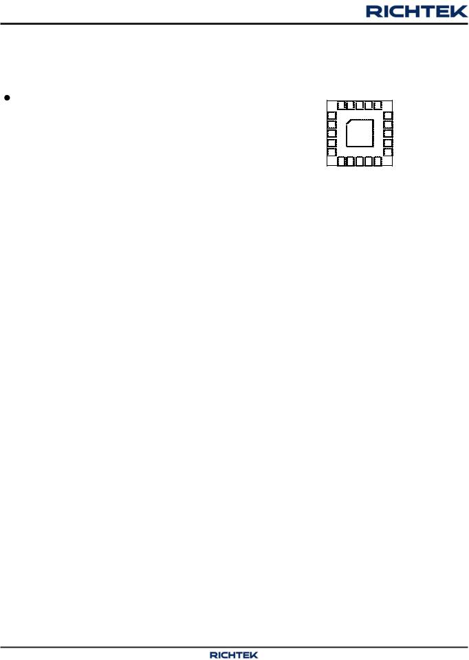
The RT8207P has all of the protection features including thermal shutdown and is available in a WQFN-20L 3x3 packages.
Applications
zDDRI/II/III/Low-Power DDRIII/DDRIV Memory Power Supplies
zNotebook Computers
zSSTL18, SSTL15 and HSTL Bus Termination
Features
zPWM Controller
`Resistor Programmable Current Limit by Low Side RDS(ON) Sense
`Quick Load Step Response Within 100ns
`1% VVDDQ Accuracy Over Line and Load
`Fixed 1.8V (DDRII), 1.5V (DDRIII) or Adjustable 0.75V to 3.3V Output Range for 1.35V (Low-Power DDRIII) and 1.2V (DDRIV)
`4.5V to 26V Battery Input Range
`Resistor Programmable Frequency
`Over/Under Voltage Protection
`Internal Current Limit Ramp Soft-Start
`Drives Large Synchronous-Rectifier FETs
`Power Good Indicator
z1.5A LDO (VTT), Buffered Reference (VTTREF)
`Capable to Sink and Source 1.5A
`External Input Available to Minimize Power Losses
`Integrated Divider Tracks 1/2 VDDQ for Both VTT and VTTREF
`Buffered Low Noise 10mA VTTREF Output
`Remote Sensing (VTTSNS)
`±20mV Accuracy for Both VTTREF and VTT
`Supports High-Z in S3 and Soft-Off in S4/S5
zRoHS Compliant and Halogen Free
Ordering Information
RT8207P 


Package Type
QW : WQFN-20L 3x3 (W-Type)
Lead Plating System
G : Green (Halogen Free and Pb Free)
Note :
Richtek products are :
`RoHS compliant and compatible with the current requirements of IPC/JEDEC J-STD-020.
`Suitable for use in SnPb or Pb-free soldering processes.
Copyright ©2013Richtek Technology Corporation. All rights reserved. |
is a registered trademark of Richtek Technology Corporation. |
DS8207P-01 October 2013 |
www.richtek.com |
|
1 |
RT8207P
Marking Information |
Pin Configurations |
|
4B= : Product Code |
4B=YM |
YMDNN : Date Code |
DNN |
|
|
|
|
(TOP VIEW) |
|
||||
|
VTT VLDOIN BOOT UGATE PHASE |
|
||||
|
20 19 |
18 17 16 |
|
|||
VTTGND |
1 |
|
|
|
15 |
LGATE |
VTTSNS |
2 |
GND |
14 |
PGND |
||
GND |
3 |
13 |
CS |
|||
VTTREF |
4 |
|
|
21 |
12 |
VDDP |
VDDQ |
5 |
|
|
|
11 |
VDD |
|
6 |
7 |
8 |
9 |
10 |
|
|
FB S3 |
S5 |
TON |
PGOOD |
|
|
|
WQFN-20L 3x3 |
|
||||
Copyright ©2013 Richtek Technology Corporation. All rights reserved. |
is a registered trademark of Richtek Technology Corporation. |
www.richtek.com |
DS8207P-01 October 2013 |
2 |
|
|
|
|
|
|
|
|
|
|
|
|
|
|
RT8207P |
Typical Application Circuit |
|
|
|
|
|
|
|
|
|
||||
|
|
|
|
|
|
|
|
|
V |
|
|
|
|
|
|
|
|
|
|
|
|
|
IN |
26V |
|
|
|
|
|
|
|
|
|
|
R |
|
4.5V to |
|
|
|
|
|
|
|
|
|
|
|
|
|
|
|
|
|
|
|
|
|
|
|
|
|
TON |
|
|
|
|
|
|
|
|
|
|
|
|
|
620k |
|
|
|
|
|
|
|
|
|
|
RT8207P |
|
R5 |
|
C9 |
|
|
|
||
|
|
|
|
|
|
10µF x 3 |
|
|
|||||
|
|
|
9 |
18 |
0 |
C4 |
|
|
|||||
|
|
|
TON |
BOOT |
|
|
|
V |
|||||
|
|
|
|
|
|
|
|
||||||
V |
|
|
12 |
|
|
|
|
|
0.1µF |
|
|
|
VDDQ |
|
|
|
|
|
|
|
|
|
|
1.2V |
|||
VDDP |
|
|
|
VDDP |
|
17 |
R6 |
0 |
|
Q1 |
|
|
|
5V |
|
|
|
UGATE |
|
|
|
|
|||||
|
R1 |
|
|
|
BSC09 |
L1 |
|
|
|||||
C1 |
|
|
|
|
|
|
|
||||||
|
|
|
|
|
|
|
|
4N03S |
1µH |
|
|
||
|
5.1 |
|
|
|
16 |
|
|
|
|
|
|||
|
1µF |
11 |
|
PHASE |
|
|
|
|
|
||||
|
VDD |
|
|
|
|
|
|
||||||
|
|
|
|
|
|
|
|
|
|
||||
|
|
C2 |
|
|
|
|
|
|
|
|
|||
|
|
|
|
15 |
|
|
|
|
|
|
C7 |
||
|
|
R3 |
|
LGATE |
|
|
|
|
R7* |
|
|||
|
|
1µF |
|
|
|
|
Q2 |
|
|
220µF |
|||
|
|
|
|
|
|
|
|
|
|
||||
|
R2 |
|
5.6k |
|
|
|
|
|
|
|
|
||
|
|
|
|
|
|
BSC032N03S |
|
C5* |
R8 |
C6* |
|||
|
100k |
|
13 |
CS |
|
|
|
|
|||||
|
|
|
|
|
|
|
|
6k |
|
||||
|
|
|
|
|
|
|
|
|
|
|
|||
|
|
|
10 |
|
6 |
|
|
|
|
|
|
||
PGOOD |
|
|
PGOOD |
FB |
|
|
|
|
|
|
|
||
|
|
|
|
|
|
* : Optional |
|
|
|||||
VTT/VTTREF Control |
|
7 |
S3 |
|
|
|
|
R9 |
C9 |
||||
|
|
|
|
|
|
|
|
||||||
|
8 |
|
19 |
|
|
|
|
|
10k |
0.1µF |
|||
|
|
|
|
VLDOIN |
|
|
|
|
|
||||
|
VDDQ Control |
|
S5 |
|
|
|
|
|
|
|
|||
|
|
|
|
|
|
|
|
|
|
||||
|
|
|
|
5 |
|
|
|
|
|
|
|
||
|
|
|
|
|
VDDQ |
|
|
|
|
|
|
|
|
|
|
|
|
|
|
|
|
|
|
|
|
|
|
|
|
|
|
|
|
20 |
|
|
|
V |
|
|
|
|
3 , 21 (Exposed Pad) |
|
VTT |
|
|
|
|
TT |
|
|
|
||
|
GND |
2 |
|
|
C8 |
0.6V |
|
|
|
||||
|
|
|
14 |
|
|
|
|
|
|
||||
|
|
|
PGND |
VTTSNS |
|
|
10µF x 2 |
|
|
|
|
||
|
|
|
|
|
|
|
|
|
|
||||
|
|
|
1 |
|
4 |
|
|
|
|
|
|
|
|
|
|
|
VTTGND |
VTTREF |
|
|
C3 |
|
|
|
|
||
|
|
|
|
|
|
|
|
|
|
|
|||
|
|
|
|
|
|
|
|
|
|
|
|
|
|
|
|
|
|
|
|
|
|
|
33nF |
|
|
|
|
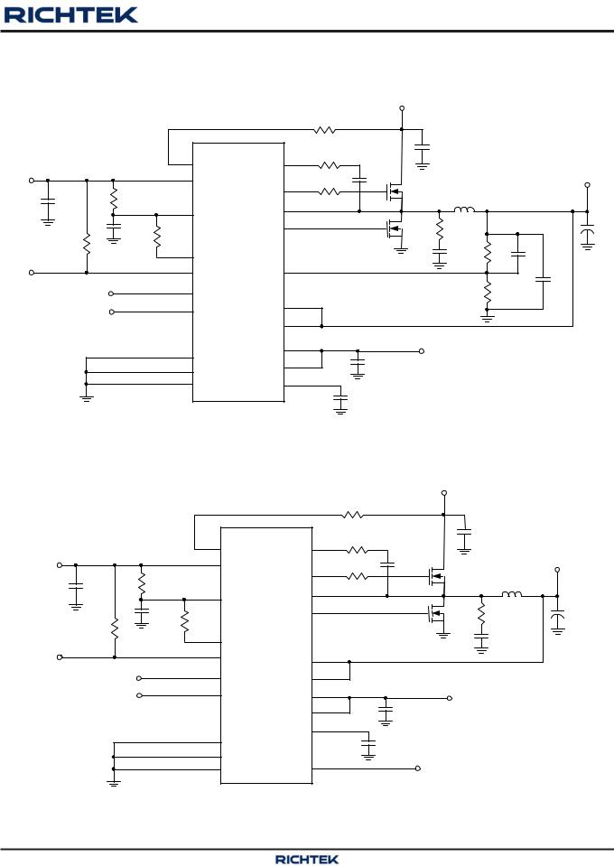
Figure 1. Adjustable Voltage Regulator
|
|
|
9 |
V |
|
|
12 |
VDDP |
|
|
|
5V |
C1 |
R1 |
|
|
|
||
|
5.1 |
|
|
|
1µF |
11 |
|
|
|
||
|
|
|
|
|
|
C2 |
R3 |
|
R2 |
1µF |
|
|
|
5.6k |
|
|
100k |
|
13 |
|
|
|
|
PGOOD |
|
|
10 |
|
|
|
|
VTT/VTTREF Control |
|
7 |
|
|
8 |
||
|
VDDQ Control |
|
|
|
|
|
|
|
3 , 21 (Exposed Pad) |
||
|
|
|
14 |
|
|
|
1 |
|
|
|
|
V |
|
|
|
|
|
|
|
|
IN |
|
26V |
|
|
|
|
|
R |
4.5V to |
|
|
|
|
|
|
|
|
|
|
|
|
|
|
|
|
TON |
|
|
|
|
|
|
|
|
620k |
|
|
|
|
|
RT8207P |
|
R5 |
|
C8 |
|
|
||
|
|
10µF x 2 |
|
|||||
18 |
0 |
C4 |
|
|
||||
TON |
BOOT |
|
V |
|||||
|
|
|
||||||
|
|
|
|
|||||
|
|
|
|
0.1µF |
|
|
|
VDDQ |
VDDP |
|
|
|
Q1 |
|
1.8V/1.5V |
||
|
17 |
R6 |
0 |
|
||||
UGATE |
|
|
||||||
|
BSC09 |
L1 |
|
|||||
|
|
|
|
|||||
|
|
|
|
|
||||
|
PHASE |
16 |
|
|
4N03S |
1µH |
|
|
VDD |
|
|
|
|
||||
|
|
|
|
|
|
|||
|
|
|
|
|
|
|
||
|
15 |
|
|
|
|
|
C6 |
|
|
LGATE |
|
|
|
R7* |
|||
|
|
|
Q2 |
|
220µF |
|||
|
|
|
|
|
|
|
||
|
|
|
|
BSC032N03S |
|
C5* |
|
|
CS |
|
|
|
|
|
|
||
|
|
|
|
|
|
|
|
|
PGOOD |
VDDQ |
5 |
|
|
|
|
|
|
|
19 |
|
|
|
* : |
Optional |
||
S3 |
VLDOIN |
|
|
|
||||
|
|
|
|
|
|
|||
|
|
|
|
|
|
|
||
S5 |
|
20 |
|
|
|
V |
|
|
VTT |
|
|
|
|
TT |
|
|
|
2 |
|
C7 |
|
0.9V/0.75V |
|
|
||
|
VTTSNS |
|
|
|
|
|||
|
|
10µF x 2 |
|
|
|
|
||
|
4 |
|
|
|
|
|
||
|
VTTREF |
|
C3 |
|
|
|
|
|
GND |
|
|
|
|
|
|
||
|
|
|
|
|
|
|
||
|
|
|
33nF |
|
|
|
|
|
PGND |
|
|
|
|
|
|
|
|
FB |
6 |
|
V |
|
for DDRII |
|
|
|
|
|
|
|
|
||||
VTTGND |
|
|
VDDP |
|
|
|
||
|
|
|
GND for DDRIII |
|
|
|||
|
|
|
|
|
|
|||
Figure 2. Fixed Voltage Regulator for
Copyright ©2013 Richtek Technology Corporation. All rights reserved. |
is a registered trademark of Richtek Technology Corporation. |
DS8207P-01 October 2013 |
www.richtek.com |
|
3 |
RT8207P
Functional Pin Description
Pin No. |
Pin Name |
Pin Function |
|
1 |
VTTGND |
Power Ground Output for VTT LDO. |
|
|
|
|
|
2 |
VTTSNS |
Voltage Sense Input for VTT LDO. Connect to the terminal of the VTT LDO |
|
output capacitor. |
|||
|
|
||
3, |
GND |
Analog Ground. The exposed pad must be soldered to a large PCB and |
|
21 (Exposed Pad) |
connected to GND for maximum thermal dissipation. |
||
4 |
VTTREF |
Buffered Reference Output. |
|
|
|
|
|
|
|
Reference Input for VTT and VTTREF. Discharge current sinking terminal for |
|
5 |
VDDQ |
VDDQ non-tracking discharge. Output voltage feedback input for VDDQ output |
|
|
|
if the FB pin is connected to VDD or GND. |
|
|
|
VDDQ Output Setting. Connect to GND for DDR3 (VVDDQ = 1.5V) power |
|
6 |
FB |
supply. Connect to VDD for DDR2 (VVDDQ = 1.8V) power supply. Or connect to |
|
a resistive voltage divider from VDDQ to GND to adjust the output of PWM from |
|||
|
|
||
|
|
0.75V to 3.3V. |
|
7 |
S3 |
S3 Signal Input. |
|
|
|
|
|
8 |
S5 |
S5 Signal Input |
|
|
|
|
|
9 |
TON |
Set the UGATE on time through a pull-up resistor connecting to VIN. |
|
10 |
PGOOD |
Power Good Open Drain Output. In High state when VDDQ output voltage is |
|
within the target range. |
|||
|
|
||
11 |
VDD |
Supply Input for Analog Supply. |
|
|
|
|
|
12 |
VDDP |
Supply Input for LGATE Gate Driver. |
|
|
|
|
|
13 |
CS |
Current Limit Threshold Setting Input. Connect to VDD through the voltage |
|
setting resistor. |
|||
|
|
||
14 |
PGND |
Power Ground for Low Side MOSFET. |
|
|
|
|
|
15 |
LGATE |
Low Side Gate Driver Output for VDDQ. |
|
|
|
|
|
16 |
PHASE |
Switch Node. External inductor connection for VDDQ and behave as the current |
|
sense comparator input for Low Side MOSFET RDS(ON) sensing. |
|||
|
|
||
17 |
UGATE |
High Side Gate Driver Output for VDDQ. |
|
18 |
BOOT |
Boost Flying Capacitor Connection for VDDQ. |
|
19 |
VLDOIN |
Power Supply for VTT LDO. |
|
|
|
|
|
20 |
VTT |
Power Output for VTT LDO. |
Copyright ©2013 Richtek Technology Corporation. All rights reserved. |
is a registered trademark of Richtek Technology Corporation. |
www.richtek.com |
DS8207P-01 October 2013 |
4 |
|

RT8207P
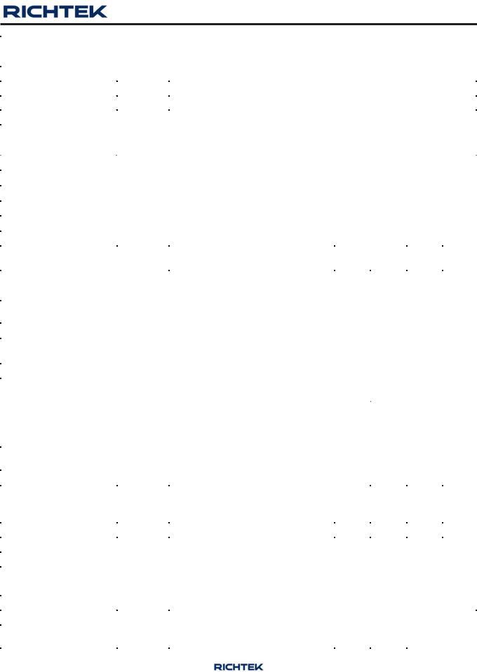
Function Block Diagram
Buck Controller
|
TRIG |
|
|
|
|
|
|
|
|
|
VDDQ |
On-time |
|
|
|
|
|
|
|
BOOT |
|
Compute |
|
|
|
|
|
|
|
|||
TON |
1-SHOT |
|
|
|
|
|
|
|
|
|
|
|
|
|
R |
|
|
|
|
||
|
|
|
|
Comp |
|
|
|
|
|
|
|
|
|
- |
|
|
|
PWM |
|
|
|
0.75V VREF |
|
+ |
|
|
S |
Q |
DRV |
UGATE |
||
|
|
|
|
|||||||
|
|
|
|
|
|
Min. TOFF |
|
|
|
PHASE |
|
|
|
Latch |
|
|
|
|
|
||
|
+ |
OV |
Q |
TRIG |
|
|
|
VDDP |
||
116%VREF |
S1 |
Q |
|
|
|
|||||
- |
|
|
1-SHOT |
|
|
|
||||
|
|
|
|
|
|
|
|
|||
FB |
+ |
UV |
Latch |
|
|
|
|
DRV |
LGATE |
|
S1 |
Q |
|
|
|
|
|||||
70% VREF |
- |
|
|
|
|
|
|
PGND |
||
|
|
|
|
|
|
|
|
|||
|
|
|
|
|
|
Diode |
|
|
|
|
|
|
|
|
- |
|
|
|
|
|
|
|
|
|
|
|
Emulation |
|
|
|
||
|
90% VREF |
+ |
|
|
|
|
||||
|
|
|
|
|
|
|
||||
|
|
|
Thermal |
|
|
|
+ |
+ |
CS |
|
VDD |
SS Timer |
|
|
|
|
GM |
|
|||
|
Shutdown |
|
|
|
+ |
- |
10µA |
|||
|
|
|
|
|
|
- |
|
|||
S5 |
|
|
|
|
|
|
|
SS Int. |
|
|
|
|
|
|
|
|
|
|
|
|
|
|
|
|
|
|
PGOOD |
|
|
|
|
|
VTT LDO
|
|
VDDQ |
|
|
S5 |
|
|
|
|
S3 |
Tracking |
Thermal |
VTTREF |
|
Discharge |
||||
|
|
Shutdown |
VLDOIN |
|
|
|
|
+ |
+ |
|
|
|
- |
|
|
|
|
- |
|
|
|
|
+ |
VTT |
|
|
|
- |
+ |
|
|
|
|
- |
VTTSNS |
|
|
- |
|
GND |
|
110% VVTTREF |
+ |
|
|
90% VVTTREF |
- |
VTTGND |
|
|
|
|||
|
|
|
+ |
|
Copyright ©2013 Richtek Technology Corporation. All rights reserved. |
is a registered trademark of Richtek Technology Corporation. |
DS8207P-01 October 2013 |
www.richtek.com |
5

RT8207P
Absolute Maximum Ratings |
(Note 1) |
|
|
|
|
|
|
|
|||
z Supply Input Voltage, TON to GND ------------------------------------------------------------------------------------- |
|
|
|
|
|
−0.3V to 32V |
|||||
z BOOT to PHASE ----------------------------------------------------------------------------------------------------------- |
|
|
|
|
|
|
|
|
−0.3V to 6V |
||
z VDD, VDDP, CS, S3, S5, VTTSNS, VDDQ, VTTREF, VTT, VLDOIN, |
|
|
|
|
|
|
|||||
FB, PGOOD to GND |
------------------------------------------------------------------------------------------------------- |
|
|
|
|
|
|
|
−0.3V to 6V |
||
z PGND, VTTGND to GND -------------------------------------------------------------------------------------------------- |
|
|
|
|
|
−0.3V to 0.3V |
|||||
z PHASE to GND |
|
|
|
|
|
|
|
|
|
|
|
DC ------------------------------------------------------------------------------------------------------------------------------ |
|
|
|
|
|
|
|
|
−1V to 32V |
||
< 20ns ------------------------------------------------------------------------------------------------------------------------ |
|
|
|
|
|
|
|
|
−8V to 38V |
||
z LGATE to GND |
|
|
|
|
|
|
|
|
|
|
|
DC ------------------------------------------------------------------------------------------------------------------------------ |
|
|
|
|
|
|
|
|
−0.3V to 6V |
||
< 20ns ------------------------------------------------------------------------------------------------------------------------ |
|
|
|
|
|
|
|
|
−2.5V to 7.5V |
||
z UGATE to PHASE |
|
|
|
|
|
|
|
|
|
|
|
DC ------------------------------------------------------------------------------------------------------------------------------ |
|
|
|
|
|
|
|
|
−0.3V to 6V |
||
< 20ns ------------------------------------------------------------------------------------------------------------------------ |
|
|
|
|
|
|
|
|
−5V to 7.5V |
||
z The Other Pins -------------------------------------------------------------------------------------------------------------- |
|
|
|
|
|
|
|
|
−0.3V to 6.5V |
||
z Power Dissipation, PD @ TA = 25°C |
|
|
|
|
|
|
|
|
|||
WQFN-20L 3x3 ------------------------------------------------------------------------------------------------------------- |
|
|
|
|
|
|
|
|
1.471W |
|
|
z Package Thermal Resistance (Note 2) |
|
|
|
|
|
|
|
|
|||
WQFN-20L 3x3, θJA -------------------------------------------------------------------------------------------------------- |
|
|
|
|
|
|
|
|
68°C/W |
|
|
WQFN-20L 3x3, θJC |
------------------------------------------------------------------------------------------------------- |
|
|
|
|
|
|
|
7.5°C/W |
|
|
z Junction Temperature ------------------------------------------------------------------------------------------------------ |
|
|
|
|
|
150°C |
|
||||
z Lead Temperature (Soldering, 10 sec.) -------------------------------------------------------------------------------- |
|
|
|
|
|
260°C |
|
||||
z Storage Temperature Range --------------------------------------------------------------------------------------------- |
|
|
|
|
|
−65°C to 150°C |
|||||
z ESD Susceptibility |
(Note 3) |
|
|
|
|
|
|
|
|
||
HBM (Human Body Model) ----------------------------------------------------------------------------------------------- |
|
|
|
|
|
2kV |
|
||||
Recommended Operating Conditions |
(Note 4) |
|
|
|
|
|
|
||||
z Supply Input Voltage, VIN ------------------------------------------------------------------------------------------------ |
|
|
|
|
|
4.5V to 26V |
|||||
z Control Voltage, VDD, VDDP -------------------------------------------------------------------------------------------- |
|
|
|
|
|
4.5V to 5.5V |
|||||
z Junction Temperature Range --------------------------------------------------------------------------------------------- |
|
|
|
|
|
−40°C to 125°C |
|||||
z Ambient Temperature Range --------------------------------------------------------------------------------------------- |
|
|
|
|
|
−40°C to 85°C |
|||||
Electrical Characteristics |
|
|
|
|
|
|
|
|
|||
(VIN = 15V, VDD = VVDDP = 5V, RTON = 1MΩ, TA = 25°C, unless otherwise specified) |
|
|
|
|
|
|
|||||
|
|
|
|
|
|
|
|
|
|
||
Parameter |
|
Symbol |
|
Test Conditions |
Min |
|
Typ |
Max |
Unit |
||
PWM Controller |
|
|
|
|
|
|
|
|
|
|
|
Quiescent Supply Current |
|
|
FB forced above the regulation point, |
-- |
|
470 |
1000 |
|
μA |
||
(VDD + VDDP) |
|
|
|
VS5 = 5V, VS3 = 0V |
|
|
|||||
|
|
|
|
|
|
|
|
|
|||
TON Operating Current |
|
|
RTON = 1MΩ |
|
-- |
|
15 |
-- |
|
μA |
|
IVLDOIN BIAS Current |
|
|
VS5 = VS3 = 5V, VTT = No Load |
-- |
|
1 |
-- |
|
μA |
||
IVLDOIN Standby Current |
|
|
VS5 = 5V, VS3 = 0V, VTT = No Load |
-- |
|
0.1 |
10 |
|
μA |
||
|
|
|
|
|
|
|
|
|
|||
|
|
|
|
|
|
|
|
|
|
|
|
Copyright ©2013 Richtek Technology Corporation. All rights reserved. |
is a registered trademark of Richtek Technology Corporation. |
|
|||||||||
www.richtek.com |
|
|
|
|
|
|
DS8207P-01 October |
2013 |
|||
6 |
|
|
|
|
|
|
|
|
|
|
|
RT8207P
Parameter |
Symbol |
Test Conditions |
Min |
Typ |
Max |
Unit |
|
PWM Controller |
|
|
|
|
|
|
|
|
|
VDD + VVDDP |
|
-- |
1 |
10 |
|
Shutdown Current |
ISHDN |
TON |
|
-- |
0.1 |
5 |
μA |
(VS5 = VS3 = 0V) |
S5/S3 = 0V |
|
−1 |
0.1 |
1 |
||
|
|
|
|||||
|
|
IVLDOIN |
|
-- |
0.1 |
1 |
|
FB Reference Voltage |
VREF |
VDD = 4.5V to 5.5V |
|
0.742 |
0.75 |
0.758 |
V |
Fixed VDDQ Output |
|
FB = GND |
|
-- |
1.5 |
-- |
V |
Voltage |
|
FB = VDD |
|
-- |
1.8 |
-- |
|
|
|
|
|||||
FB Input Bias Current |
|
FB = 0.75V |
|
−1 |
0.1 |
1 |
μA |
VDDQ Voltage Range |
|
|
|
0.75 |
-- |
3.3 |
V |
|
|
|
|
|
|
|
|
On-Time |
|
RTON = 1MΩ, VVDDQ = 1.25V |
267 |
334 |
401 |
ns |
|
Minimum Off-Time |
|
|
|
250 |
400 |
550 |
ns |
|
|
|
|
|
|
|
|
VDDQ Input Resistance |
|
|
|
-- |
100 |
-- |
kΩ |
|
|
|
|
|
|
|
|
VDDQ Shutdown |
|
VS5 = GND |
|
-- |
15 |
-- |
Ω |
Discharge Resistance |
|
|
|||||
Current Sensing |
|
|
|
|
|
|
|
CS Sink Current |
|
VCS > 4.5V |
|
9 |
10 |
11 |
μA |
Current Limit Comparator |
|
(VVDD−CS – VGND−PHASE), |
−15 |
-- |
15 |
mV |
|
Offset |
|
RCS = 10kΩ |
|
|
|
|
|
Zero Crossing Threshold |
|
GND − PHASE |
|
−5 |
-- |
10 |
mV |
|
|
|
|
|
|
|
|
Current Limit Threshold |
|
VDD – VCS |
|
50 |
-- |
200 |
mV |
Setting Range |
|
|
|||||
Fault Protection |
|
|
|
|
|
|
|
Under Voltage Protection |
VUVP |
|
|
60 |
70 |
80 |
% |
Threshold |
|
|
|||||
Over Voltage Protection |
VOVP |
With respect to error comparator |
113 |
116 |
120 |
% |
|
Threshold |
threshold |
|
|||||
Over Voltage Fault Delay |
|
FB forced above over voltage |
-- |
20 |
-- |
μs |
|
|
threshold |
|
|||||
|
|
|
|
|
|
|
|
VDD POR Threshold |
|
Rising edge, hysteresis = 120mV, |
3.9 |
4.2 |
4.5 |
V |
|
|
PWM disabled below this level |
||||||
|
|
|
|
|
|
||
Under Voltage Blank Time |
|
From S5 signal going high |
-- |
5 |
-- |
ms |
|
|
|
|
|
|
|
|
|
Thermal Shutdown |
TSD |
|
|
-- |
165 |
-- |
°C |
Thermal Shutdown |
TSD |
|
|
-- |
10 |
-- |
°C |
Hysteresis |
|
|
|||||
Driver On-Resistance |
|
|
|
|
|
|
|
UGATE Driver Source |
RUGATEsr |
BOOT − PHASE Forced to 5V |
-- |
2.5 |
5 |
Ω |
|
UGATE Driver Sink |
RUGATEsk |
BOOT − PHASE Forced to 5V |
-- |
1.5 |
3 |
Ω |
|
LGATE Driver Source |
RLGATEsr |
DL, High State |
|
-- |
2.5 |
5 |
Ω |
LGATE Driver Sink |
RLGATEsk |
DL, Low State |
|
-- |
0.8 |
1.6 |
Ω |
Dead Time |
|
LGATE Rising (PHASE = 1.5V) |
-- |
40 |
-- |
ns |
|
|
UGATE Rising |
|
-- |
40 |
-- |
||
|
|
|
|
||||
Internal Boost Charging |
|
VDDP to BOOT, 10mA |
|
-- |
-- |
80 |
Ω |
Switch On Resistance |
|
|
|||||
|
|
|
|
|
|
|
|
|
|
|
|
|
|
|
|
Copyright ©2013 Richtek Technology Corporation. All rights reserved. |
is a registered trademark of Richtek Technology Corporation. |
||||||
DS8207P-01 October 2013 |
|
|
|
|
|
www.richtek.com |
|
|
|
|
|
|
|
|
7 |
RT8207P
Parameter |
Symbol |
|
|
Test Conditions |
|
Min |
Typ |
Max |
Unit |
|||||||
Logic I/O |
|
|
|
|
|
|
|
|
|
|
|
|
|
|
|
|
Logic Input Low Voltage |
|
S3, S5 Low |
|
|
|
|
|
|
|
-- |
-- |
0.8 |
V |
|||
Logic Input High Voltage |
|
S3, S5 High |
|
|
|
|
|
|
|
2 |
-- |
-- |
V |
|||
|
|
|
|
|
|
|
|
|
|
|
|
|
||||
Logic Input Current |
|
S3, S5 = VDD/GND |
|
|
|
|
−1 |
0 |
1 |
μA |
||||||
PGOOD (upper side threshold decide by Over Voltage threshold) |
|
|
|
|
|
|
||||||||||
Trip Threshold (Falling) |
|
Measured at FB, with respect to |
|
−13 |
−10 |
−7 |
% |
|||||||||
|
reference, no load |
|
|
|
|
|
||||||||||
|
|
|
|
|
|
|
|
|
|
|
||||||
Trip Threshold (Hysteresis) |
|
|
|
|
|
|
|
|
|
|
|
|
-- |
3 |
-- |
% |
|
|
|
|
|
|
|
|
|
|
|
|
|||||
Fault Propagation Delay |
|
Falling edge, FB forced |
below |
|
-- |
2.5 |
-- |
μs |
||||||||
|
PGOOD trip threshold |
|
|
|
|
|||||||||||
|
|
|
|
|
|
|
|
|
|
|||||||
Output Low Voltage |
|
ISINK = 1mA |
|
|
|
|
|
|
|
-- |
-- |
0.4 |
V |
|||
Leakage Current |
ILEAK |
High state, forced to 5V |
|
|
|
|
-- |
-- |
1 |
μA |
||||||
VTT LDO |
|
|
|
|
|
|
|
|
|
|
|
|
|
|
|
|
|
|
VVDDQ = VLDOIN = 1.2V/1.35/1.5V/1.8V, |
−20 |
-- |
20 |
|
||||||||||
|
|
IVTT = 0A |
|
|
|
|
|
|
|
|
|
|
|
|||
|
|
VVDDQ = VLDOIN = 1.2V/1.35/1.5V/1.8V, |
−30 |
-- |
30 |
|
||||||||||
VTT Output Tolerance |
VVTTTOL |
IVTT < 1A |
|
|
|
|
|
|
|
|
|
|
mV |
|||
VVDDQ = VLDOIN = 1.2V/1.35, |
|
−40 |
-- |
40 |
||||||||||||
|
|
|
|
|||||||||||||
|
|
IVTT < 1.2A |
|
|
|
|
|
|
|
|
||||||
|
|
|
|
|
|
|
|
|
|
|
|
|
||||
|
|
VVDDQ = VLDOIN = 1.5V/1.8V, |
|
−40 |
-- |
40 |
|
|||||||||
|
|
IVTT < 1.5A |
|
|
|
|
|
|
|
|
|
|
|
|||
|
|
VVDDQ |
|
|
|
|
|
|
|
|
|
|
|
|||
|
|
VTT = |
|
|
|
|
× |
0.95 |
|
|
|
|
1.6 |
2.6 |
3.6 |
|
|
|
|
2 |
|
|
|
|
|
|
|||||||
VTT Source Current Limit |
IVTTOCLSRC |
|
|
|
|
|
|
|
|
|
A |
|||||
PGOOD = High |
|
|
|
|
|
|
|
|
|
|
||||||
|
|
VTT = 0V |
|
|
|
|
|
|
|
|
|
-- |
1.3 |
-- |
|
|
|
|
VVDDQ |
|
|
|
|
|
|
|
|
|
|
|
|||
|
|
VTT = |
|
|
|
|
×1.05 , |
|
|
|
|
|
|
|
|
|
|
|
|
2 |
|
|
|
|
|
1.6 |
2.6 |
3.6 |
|
||||
VTT Sink Current Limit |
IVTTOCLSNK |
|
|
|
|
|
|
|
|
|
A |
|||||
PGOOD = High |
|
|
|
|
|
|
|
|
|
|
||||||
|
|
|
|
|
|
|
|
|
|
|
|
|
||||
|
|
VTT = VVDDQ |
|
|
|
|
|
|
|
-- |
1.3 |
-- |
|
|||
VTT Leakage Current |
IVTTLK |
S5 = 5V, S3 = 0V, |
VTT |
|
VVDDQ |
−10 |
-- |
10 |
μA |
|||||||
= |
|
|
|
|||||||||||||
|
2 |
|||||||||||||||
|
|
|
|
|
|
|
|
|
|
|
|
|
|
|
||
VTTSNS Leakage Current |
IVTTSNSLK |
ISINK = 1mA |
|
|
|
|
|
|
|
−1 |
-- |
1 |
μA |
|||
VTT Discharge Current |
IDSCHRG |
VVDDQ = 0V, VTT = 0.5V, S5 = S3 =0V |
10 |
30 |
-- |
mA |
||||||||||
VTTREF Output Voltage |
VVTTREF |
|
|
VVDDQ |
|
|
|
|
-- |
0.9 / |
-- |
V |
||||
VVTTREF = |
2 |
|
|
|
|
|
0.75 |
|||||||||
|
|
|
|
|
|
|
|
|
|
|
|
|
||||
|
|
VLDOIN = VVDDQ = 1.5V, |
|
|
−15 |
-- |
15 |
|
||||||||
VDDQSNS/2, VTTREF |
|
IVTTREF <10mA |
|
|
|
|
|
|||||||||
VVTTREFTOL |
|
|
|
|
|
|
|
mV |
||||||||
Output Voltage Tolerance |
VLDOIN = VVDDQ = 1.8V, |
|
|
|
|
−18 |
-- |
18 |
||||||||
|
|
IVTTREF <10mA |
|
|
|
|
|
|||||||||
|
|
|
|
|
|
|
|
|
|
|||||||
VTTREF Source Current |
IVTTREFOCL |
VVTTREF = 0V |
|
|
|
|
|
|
|
10 |
40 |
80 |
mA |
|||
Limit |
|
|
|
|
|
|
|
|||||||||
|
|
|
|
|
|
|
|
|
|
|
|
|
|
|
|
|
Copyright ©2013 Richtek Technology Corporation. All rights reserved. |
is a registered trademark of Richtek Technology Corporation. |
www.richtek.com |
DS8207P-01 October 2013 |
8 |
|
 Loading...