


 Loading...
RICHTEK RT9163-33CL, RT9163-33CX, RT9163-33CXL, RT9163-33CZL, RT9163-35CG Datasheet
...
RT9163
500mA Low Dropout Positive Voltage Regulator
General Description
The RT9163 is a positive low dropout regulator designed for applications requiring low dropout performance at full rated current. The device is available in fixed output voltage of 3.3V, 3.5V, and 5.0V. The RT9163 provides excellent regulation over line, load, and temperature variations.
The other features include low dropout performance at a maximum of 1.4V at 500mA, fast transient response, internal current limiting, and thermal shutdown protection of the output devices. The RT9163 is a three-terminal regulator available in surface mount SOT-89, SOT-223, and TO-252 packages.
Applications
z5V to 3.3V Linear Regulator
zLow Voltage Microcontroller, DSP… etc Power Supply
zLinear Regulator for LAN Card and CD-ROM
Ordering Information
RT9163-
 Package type ZL : TO-92 X : SOT-89
XL : SOT-89, L Type L : TO-252
G : SOT-223 Type I
GL : SOT-223 Type II
GT : SOT-223 Type III
GF : SOT-223 Type IV Operating temperature range C: Commercial standard Output voltage
33 : 3.3V
35 : 3.5V
50 : 5.0V
Features
zLow Dropout, Maximum 1.4V at 500mA
zFast Transient Response
z±2% Total Output Regulation
z0.4% Line Regulation
z0.4% Load Regulation
zTO-92, SOT-89, SOT-223, and TO-252 Packages
Pin Configurations
Part Number |
|
|
Pin Configurations |
|||||||||||
|
|
|
|
|
|
|
|
|
|
|
|
|
|
|
RT9163CZL |
|
|
|
|
|
|
|
|
|
|
|
|
TOP VIEW |
|
|
|
|
|
|
|
|
|
|
|
|
|
|||
|
|
|
|
|
|
|
|
|
|
|
|
|||
(Plastic TO-92) |
|
|
|
|
|
|
|
|
|
|
|
1. |
VIN |
|
|
|
|
|
|
|
|
|
|
|
2. |
GND |
|||
|
|
|
|
|
|
|
|
|
|
3. |
VOUT |
|||
|
|
|
|
|
|
|
|
|
|
|
|
|
|
|
|
|
|
1 |
|
2 |
|
|
|
3 |
|
|
|
|
|
|
|
|
|
|
|
|
|
|
|
|
|
|
|
|
RT9163CX |
|
|
|
TOP VIEW |
|
(Plastic SOT-89) |
|
|
|
1. |
VOUT |
|
|
|
|
2. |
GND (TAB) |
|
1 |
2 |
3 |
3. |
VIN |
RT9163CXL |
|
|
|
TOP VIEW |
|
(Plastic SOT-89) |
|
|
|
1. |
GND |
|
|
|
|
2. |
VIN (TAB) |
|
1 |
2 |
3 |
3. VOUT |
|
|
|
|
|
||
RT9163CL |
|
|
|
TOP VIEW |
|
(Plastic TO-252) |
|
|
|
1. VOUT |
|
|
|
|
|
2. GND (TAB) |
|
|
1 |
2 |
3 |
3. |
VIN |
|
|
|
|||
RT9163CG |
|
|
|
TOP VIEW |
|
(Plastic SOT-223) |
|
|
|
1. |
VOUT |
Type I |
|
|
|
2. |
GND (TAB) |
1 |
2 |
3 |
3. VIN |
||
RT9163CGL |
|
|
|
TOP VIEW |
|
(Plastic SOT-223) |
|
|
|
1. |
VIN |
Type II |
|
|
|
2. |
GND (TAB) |
1 |
2 |
3 |
3. VOUT |
||
RT9163CGT |
|
|
|
TOP VIEW |
|
(Plastic SOT-223) |
|
|
|
1. |
GND |
Type III |
|
|
|
2. |
VOUT (TAB) |
1 |
2 |
3 |
3. VIN |
||
RT9163CGF |
|
|
|
TOP VIEW |
|
(Plastic SOT-223) |
|
|
|
1. |
GND |
Type IV |
|
|
|
2. |
VIN (TAB) |
1 |
2 |
3 |
3. VOUT |
||
DS9163-14 April 2002 |
www.richtek-ic.com.tw |
|
1 |
RT9163
Marking Information
Part Number |
|
|
|
|
|
|
|
Marking |
|
|
|
|
|
|
|
|
|
|
|
|
|
|
|
|
|
|
|
|
|
|
|
|||||||||||
RT9163-33CZL |
|
|
|
|
|
|
|
RTAJ |
|
|
|
|
|
|
|
|
|
|
|
|
|
|
|
|
|
|
|
|
|
|
|
|
|
|
|
|
|
|
|
|||
RT9163-35CZL |
|
|
|
|
|
|
|
RTAK |
|
|
|
|
|
|
|
|
|
|
|
|
|
|
|
|
|
|
|
|
|
|
|
|
|
|
|
|
|
|
|
|||
RT9163-50CZL |
|
|
|
|
|
|
|
RTA1 |
|
|
|
|
|
|
|
|
|
|
|
|
|
|
|
|
|
|
|
|
|
|
|
|
|
|
|
|
|
|
|
|||
RT9163-33CX |
|
|
|
|
|
|
|
|
A8 |
|
|
|
|
|
|
|
|
|
|
|
|
|
|
|
|
|
|
|
|
|
|
|
|
|
|
|
|
|
|
|
||
RT9163-35CX |
|
|
|
|
|
|
|
|
A9 |
|
|
|
|
|
|
|
|
|
|
|
|
|
|
|
|
|
|
|
|
|
|
|
|
|
|
|
|
|
|
|
||
RT9163-50CX |
|
|
|
|
|
|
|
|
AT |
|
|
|
|
|
|
|
|
|
|
|
|
|
|
|
|
|
|
|
|
|
|
|
|
|
|
|
|
|
|
|
||
RT9163-33CXL |
|
|
|
|
|
|
|
|
CK |
|
|
|
|
|
|
|
|
|
|
|
|
|
|
|
|
|
|
|
|
|
|
|
|
|
|
|
|
|
|
|
||
RT9163-35CXL |
|
|
|
|
|
|
|
|
CL |
|
|
|
|
|
|
|
|
|
|
|
|
|
|
|
|
|
|
|
|
|
|
|
|
|
|
|
|
|
|
|
||
RT9163-50CXL |
|
|
|
|
|
|
|
|
CM |
|
|
|
|
|
|
|
|
|
|
|
|
|
|
|
|
|
|
|
|
|
|
|
|
|
|
|
|
|
|
|
||
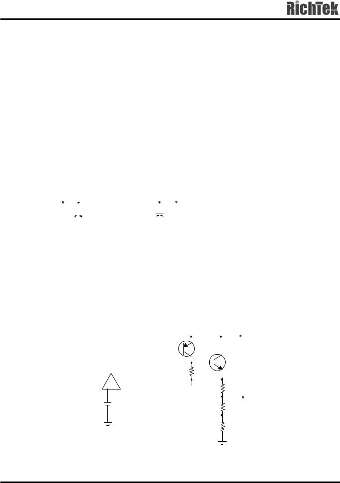
Typical Application Circuit |
|
|
|
|
|
|
|
|
|
|
|
|
|
|
|
|
|
|
|
|
||||||||||||||||||||||
|
|
|
|
|
|
|
|
|
|
|
|
|
|
|
|
|
|
|
|
|
|
|
|
|
|
|
|
|
|
|
|
|
|
|
|
|
|
|
|
|
|
|
|
VIN |
|
|
|
|
|
|
|
|
|
|
RT9163 |
|
|
|
|
|
|
|
|
|
|
|
VOUT |
||||||||||||||||||
|
|
|
|
|
|
|
|
|
VIN |
|
|
|
|
|
|
|
VOUT |
|
|
|
|
|
|
|
|
|
|
|
||||||||||||||
|
|
|
|
|
+ |
|
|
|
|
|
|
|
|
|
|
|
|
+ C2 |
||||||||||||||||||||||||
|
|
C1 |
|
|
|
|
|
GND |
|
|
|
|
|
|
|
|
|
|
|
|
|
|
|
|||||||||||||||||||
|
|
|
|
|
|
|
|
|
|
|
|
|
|
|
|
_ 10 F |
|
|
|
|
|
|
|
|
|
|||||||||||||||||
|
10 F |
|
_ |
|
|
|
|
|
|
|
|
|
|
|
|
|
|
|
|
|
|
|
|
|
|
|
|
|
|
|
|
|||||||||||
Pin Description |
|
|
|
|
|
|
|
|
|
|
|
|
|
|
|
|
|
|
|
|
|
|
|
|
|
|
|
|
|
|
|
|
|
|
|
|
|
|
|
|||
Pin Name |
|
|
|
|
|
Pin Function |
|
|
|
|
|
|
|
|
|
|
|
|
|
|
|
|
|
|
|
|
||||||||||||||||
VOUT |
Output Voltage |
|
|
|
|
|
|
|
|
|
|
|
|
|
|
|
|
|
|
|
|
|
|
|
|
|
|
|
|
|
|
|
||||||||||
GND |
Ground |
|
|
|
|
|
|
|
|
|
|
|
|
|
|
|
|
|
|
|
|
|
|
|
|
|
|
|
|
|
|
|
|
|
|
|
|
|
|
|
||
VIN |
Power Input |
|
|
|
|
|
|
|
|
|
|
|
|
|
|
|
|
|
|
|
|
|
|
|
|
|
|
|
|
|
|
|
||||||||||
Function Block Diagram |
|
|
|
|
|
|
|
|
|
|
|
|
|
|
|
|
|
|
|
|
|
|
|
|
|
|
|
|
|
|
|
|||||||||||
|
|
|
|
|
|
|
|
|
|
|
|
|
|
|
|
|
|
|
|
|
|
|
|
|
|
|
|
|
|
|
|
|
|
|
|
|
|
|
|
|
|
VIN |
|
|
|
|
|
|
|
|
|
|
|
|
|
|
|
|
|
|
|
|
|
|
|
|
|
|
|
|
|
|
|
|
|
|
|
|
|
Q2 |
|
|
|||
|
|
|
|
|
|
|
|
|
|
|
|
|
|
|
|
|
|
|
|
|
|
|
|
|
|
|
|
|
|
|
|
|
|
|
|
|
|
|
|
|
||
|
|
|
|
|
|
|
|
|
|
|
|
|
Buffer |
|
|
|
|
|
|
|
|
|
|
|
|
|
|
|
|
|
|
|||||||||||
|
|
|
|
|
|
|
|
|
|
|
|
|
|
|
|
|
|
|
|
|
|
|
|
|
|
|||||||||||||||||
|
|
|
|
|
|
|
|
|
|
|
|
Amplifier |
|
|
|
Thermal |
|
|
|
|
|
|
|
|
Q1 |
|||||||||||||||||
|
|
|
|
|
|
|
|
|
|
|
|
|
|
|
|
|
|
|
|
|
||||||||||||||||||||||
|
|
|
|
|
|
|
|
|
|
|
|
|
|
|
|
|
|
|
|
|
|
|
Shutdown |
|
|
|
|
|
|
R4 |
|
|||||||||||
|
|
|
|
|
|
|
|
|
|
|
|
|
|
|
|
|
|
|
|
|
|
|
|
|
|
|
|
|
||||||||||||||
|
|
|
|
|
|
|
|
|
|
|
|
|
|
|
|
|
|
|
|
|
|
|
|
|
|
|
|
|
|
|
|
|||||||||||
|
|
|
|
|
|
|
|
Error |
|
|
|
|
|
|
|
|
|
|
|
|
|
|
|
|
|
|
|
|
|
|
|
|
|
|
|
|||||||
|
|
|
|
|
|
|
|
|
|
|
|
|
|
|
|
|
|
|
|
|
|
|
|
|
|
|
|
|
|
|
|
|||||||||||
|
|
|
|
|
|
|
|
|
|
|
|
|
|
|
|
|
|
|
|
|
|
|
|
|
|
|
|
|
|
|
|
|
|
|
|
|
||||||
|
|
|
|
|
|
|
|
Amplifier |
_ |
|
|
|
|
|
|
|
|
|
Current |
|
|
|
|
|
|
|
|
|
|
|
||||||||||||
|
|
|
|
+ |
|
|
|
|
|
|
|
|
|
|
|
|
|
|
|
|
R3 |
|||||||||||||||||||||
|
|
|
|
|
|
|
|
|
|
|
|
|
|
|
|
|
|
|||||||||||||||||||||||||
|
|
|
|
|
|
|
|
|
|
|
|
|
|
|
|
Limiting |
|
|
|
|
|
|
|
|||||||||||||||||||
|
|
|
|
|
|
|
|
|
|
|
|
|
|
|
|
|
|
|
|
|
|
|
|
|
|
|
|
|
|
|
|
|
VOUT |
|||||||||
|
|
|
|
|
|
|
|
|
VREF |
|
|
|
|
|
|
|
|
|
|
|
|
Sensor |
|
|
|
|
|
|
|
|
|
|||||||||||
|
|
|
|
|
|
|
|
|
|
|
|
|
|
|
|
|
|
|
|
|
|
|
|
|
|
|
|
|
|
|
||||||||||||
|
|
|
|
|
|
|
|
|
|
|
|
|
|
|
|
|
|
|
|
|
|
|
|
|
|
|
|
|
|
|
|
|
|
|
|
|
R1 |
|||||
|
|
|
|
|
|
|
|
|
|
|
|
|
|
|
|
|
|
|
|
|
|
|
|
|
|
|
|
|
|
|
|
|
|
|
|
|
|
|
|
R2 |
||
|
|
|
|
|
|
|
|
|
|
|
|
|
|
|
|
|
|
|
|
|
|
|
|
|
|
|
|
|
|
|
|
|
|
|
|
|
|
|
|
|||
|
|
|
|
|
|
|
|
|
|
|
|
|
|
|
|
|
|
|
|
|
|
|
|
|
|
|
|
|
|
|
|
|
|
|
|
|
|
|
|
|||
www.richtek-ic.com.tw |
DS9163-14 April 2002 |
2

RT9163
Absolute Maximum Ratings
zInput Voltage


 15V
15V
zPower Dissipation, PD @ TA = 25°C
TO-92 


 0.6W SOT-89


 0.5W
0.5W
zPackage Thermal Resistance
TO-92, θJA 


 160°C/W SOT-89, θJC


 100°C/W SOT-89, θJA


 300°C/W SOT-223, θJC


 15°C/W SOT-223, θJA


 60°C/W TO-252, θJC


 15°C/W TO-252, θJA


 56°C/W
zOperating Junction Temperature Range


 −40°C to 125°C
zStorage Temperature Range 


 −65°C to 150°C
Electrical Characteristics
(VIN = 5V, TA = 25°C, unless otherwise specified)
Parameter |
|
Symbol |
Test Conditions |
Min |
Typ |
Max |
Units |
|
|
RT9163-33 |
|
|
3.235 |
3.300 |
3.365 |
|
|
Output Voltage (1) |
RT9163-35 |
VOUT |
|
3.430 |
3.500 |
3.570 |
V |
|
|
RT9163-50 |
|
VIN = 7A |
4.900 |
5.000 |
5.100 |
|
|
Line Regulation (1) |
RT9163-33 |
|
VIN = 5V ~ 15V |
-- |
0.1 |
0.4 |
|
|
RT9163-35 |
∆VLINE |
% |
||||||
|
|
|
|
|||||
|
RT9163-50 |
|
VIN = 7V ~ 15V |
-- |
0.1 |
0.4 |
|
|
Load Regulation (1) |
|
∆VLOAD |
IL = 0 ~ 500mA |
-- |
0.2 |
0.4 |
% |
|
Dropout Voltage (2) |
|
VDROP |
∆VOUT = 1% |
-- |
1.3 |
1.4 |
V |
|
Current Limit |
|
ILIMIT |
Load = 1Ω |
550 |
-- |
-- |
mA |
|
Quiescent Current |
|
IQ |
|
-- |
4.5 |
8 |
mA |
|
Temperature Coefficient |
|
TC |
|
-- |
0.005 |
-- |
%/°C |
|
Temperature Stability |
|
TS |
|
-- |
0.5 |
-- |
% |
|
RMS Output Noise (3) |
|
|
|
-- |
0.003 |
-- |
%/VOUT |
Notes:
(1)Low duty cycle pulse tested with Kelvin connections.
(2)Dropout voltage is defined as the input to output differential at which the output voltage drops 100mV below the value measured with a 1V differential.
(3)Bandwidth of 10 Hz to 10 kHz.
DS9163-14 April 2002 |
www.richtek-ic.com.tw |
|
3 |
Loading...