


QUICK LOGIC QL82SD-4PT280C, QL82SD-4PT280I, QL82SD-4PT280M, QL82SD-5PB516C, QL82SD-5PB516M Datasheet
...QL82SD Device Data Sheet
• • • • • • |
|
Device Highlights |
Extended Features |
LVDS SERDES Basic Features |
The following can be implemented into the |
programmable logic: |
•10 High Speed Bus LVDS Serial Links— bandwidth up to 5 Gbps
•Eight Independent Bus LVDS serial transceivers with operating speeds to 632 Mbps per channel
•Two Independent Bus LVDS clock serial transceivers with operating speeds to 400 MHz per channel
•Integrated clock and data recovery (CDR) with no external analog components required
•CDR bypass for applications with external clock source
•Programmable serial to parallel configuration
•10-bit data width—with
•clock recovery
•4-bit, 7-bit and 8-bit data widths— with external clock
•1-bit asynchronous level conversion
•Fast Lock and Random (auto) Lock capable
•Lock signal feedback
•I/O support for LVTTL, LVCMOS, PCI, GTL+, SSTL2, SSTL3, LVDS, LVPECL
•Low Power/Independent power-down mode for each SERDES channel
•IEEE1149.1 JTAG Support & boundary scan
•Operation over PCB or backplane traces, or across twisted pair cabling up to 25 m
•Point-to-Point, Multi-Point, and Multi-Drop Support
•Pre-Emphasis Control on each LVDS Channel Link
•UTOPIA Level 2, 16-bit wide System interface (up to 50 MHz) with parity support for ATM applications
•UTOPIA Level 3 compatible 8-bit wide system Interface (up to 100 MHz) with parity support for ATM applications
•CSIX-L1 32-bit switch fabric interface (up to 100 MHz)
•Supports Generic 8,16,32-bit microprocessor bus interface for configuration, control and status monitoring
•Supports Generic 32, 64-bit peripheral bus interface for bridging functions
Flexible Programmable Logic
•2,016 Programmable Logic Cells
•536 K System Gates
•Muxed architecture; non-volatile technology
•Completely customizable for any digital application
Dual Port SRAM Blocks
•36 Dual Port SRAM Blocks
•Configurable array sizes (by 2, 4, 9, 18)
•< 3 ns access times, FIFO capable of over 300 MHz
•Configurable as RAM or FIFO
|
|
|
• |
|
|
Preliminary |
|
• |
|
© 2002 QuickLogic Corporation |
www.quicklogic.com • |
1 |
||
|
|
|
• |
|
|
|
|
• |
|
|
|
|
• |
|
QL82SD Device Data Sheet Rev C
Programmable I/O
•Up to 252 Programmable I/O pins
•High performance Enhanced I/O (EIO): Less than 3 ns Tco
•Programmable Slew Rate Control
•Programmable I/O Standards
•LVTTL, LVCMOS, PCI, GTL+, SSTL2, and SSTL3, LVDS, LVPECL
•Four Independent I/O Banks
•Three Register Configuration: Input, Output, OE
Embedded Computational Unit (ECU) Blocks
•Integrated multiply, add, and accumulate function
•18 distributed MAC blocks
•8 × 8 multiply (sign & unsigned)
•16-bit carry add
Advanced Clock Network
•Nine Global Clock Networks consisting of:
•one dedicated
•eight programmable
•Eight I/O (high drive) networks: two I/Os per bank
•Ten Quad-Net Networks—five per quadrant
|
|
IO Block |
|
|
IO Block |
|
|
||
|
|
|
|
RAM Blocks |
|
|
|
|
|
IO Block |
Embedded Computational Units (ECUs) |
IO Block |
|||||||
|
2016 Logic Cells |
|
|||||||
|
|
|
|
||||||
|
|
|
|
RAM Blocks |
|
|
|
|
|
|
|
LVDS/SERDES IO Block |
|
|
|||||
CH0 |
CH1 |
CH2 |
CH3 |
CLKA |
CLKB |
CH4 |
CH5 |
CH6 |
CH7 |
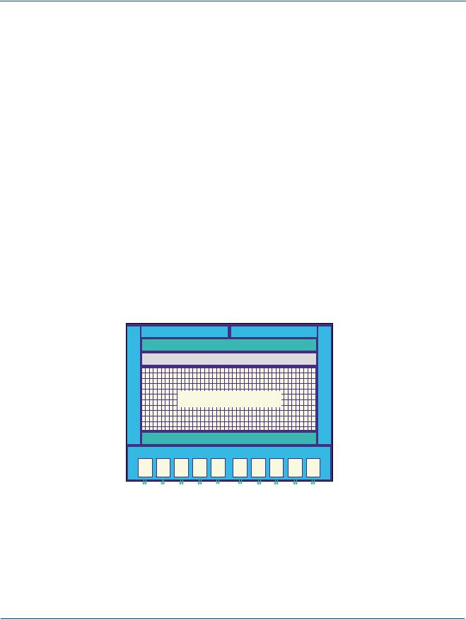
Figure 1: QL82SD Device Block Diagram
Table 1: QL82SD Device Table
Customer Part # |
SERDES |
LVDS |
SRAM |
Logic |
ECU |
Programmable I/O |
|
Data |
Clocks |
Blocks |
Cells |
Blocks |
|||
|
|
||||||
|
|
|
|
|
|
|
|
QL82SD-PQ208 |
4 |
2 |
36 |
2016 |
18 |
75 |
|
|
|
|
|
|
|
|
|
QL82SD-PT280 |
8 |
2 |
36 |
2016 |
18 |
121 |
|
|
|
|
|
|
|
|
|
QL82SD-PS484 |
8 |
2 |
36 |
2016 |
18 |
209 |
|
|
|
|
|
|
|
|
|
QL82SD-PB516 |
8 |
2 |
36 |
2016 |
18 |
252 |
|
|
|
|
|
|
|
|
•
•
2 •• www.quicklogic.com Preliminary © 2002 QuickLogic Corporation
•
•
QL82SD Device Data Sheet Rev C
General Description
LVDS SERDES Transmitter and Receiver
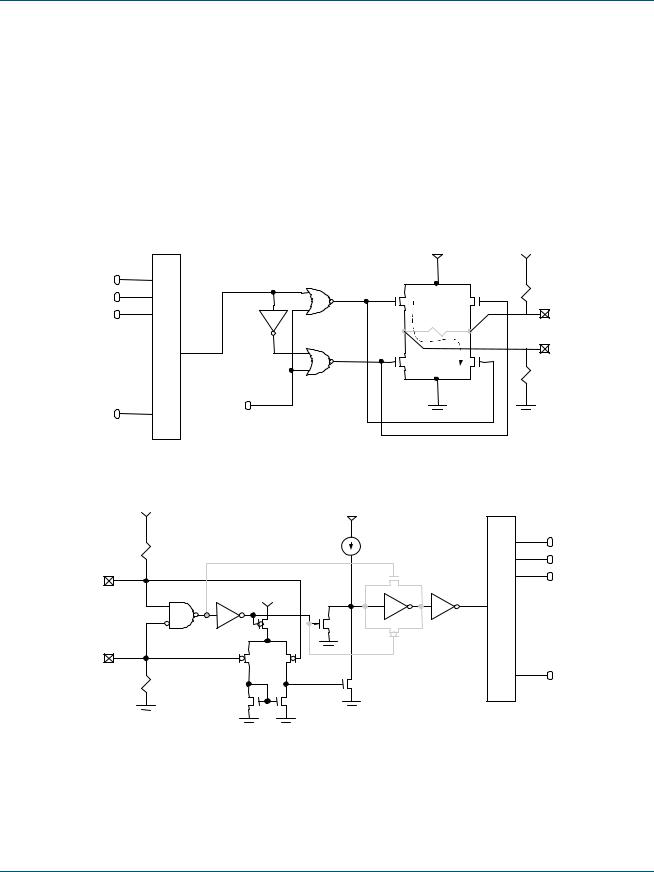
A QuickSD LVDS SERDES device in serializer mode takes a parallel data bus and a separate clock and converts them into a serial data stream. In deserializer mode, it takes a serial data stream and converts it to a configurable bit wide parallel data bus and separate clock. The reduced number of I/O board traces and cable connectors saves on cost and significantly simplifies design. Skew and timing issues are significantly reduced and performance is enhanced. Figure 2 and Figure 3 illustrate the block diagrams of the QuickSD device transmitter and receiver.
Parallel to Serial
300k
 RL = 27 Ω - 100 Ω
Do +
.
.
txd [9:0]
.
.
Vo - |
|
Vo + |
|
IL = 8-12 mA |
Do - |
|
|
|
|
|
300k |
/Enable
Figure 2: LVDS SERDES Transmitter Block Diagram
Serial to Parallel
FPGA
300k W
Din + |
. |
|
|
|
TTL_Din |
VCM = 0.2 V - 2.2 V |
. |
|
. rxd [9:0] |
Din - |
. |
|
|
300k W |
|
Figure 3: LVDS SERDES Receiver Block Diagram
© 2002 QuickLogic Corporation
Preliminary
•
www.quicklogic.com •
•• 3
•
•

QL82SD Device Data Sheet Rev C
LVDS SERDES Applications
The QuickSD device is designed to address the need for high-speed serial communications. It maintains the features of standard discrete SERDES devices, but integrates these features with customizable logic to allow for the highest degree of flexibility, performance, and integration at the lowest cost. The QuickSD device is designed to support both transmit and receive requirements in a single chip. The device can support multiple channels in a variety of modes (with or without clock recovery,) a variety of translation widths (1:1 to 1:10), as well as a range of frequencies. These capabilities make this device ideal in applications where the performance is critical and customization is required.
The QuickSD device targets three applications: on-board, board-to-board (via common backplane), and box-to-box (via common cable).
Software Support
The turnkey QuickWorks package from QuickLogic provides the most complete ESP and FPGA software solution from design entry to logic synthesis, to place and route, and to simulation. The package provides a solution for designers who use third-party tools from Cadence, Mentor, OrCAD, Synopsys, Viewlogic, Veribest and other third-party tools for design entry, synthesis, or simulation. A power calculator is also provided for SERDES power consumption.
To speed up the QuickSD design process, QuickLogic includes a SERDES Wizard in its QuickWorks package. This wizard simplifies the process of configuring the multi-channel SERDES core into each of its modes. For details on the SERDES Wizard, please refer to "The QL82SD Quickstart Design Guide". To find this guide go to the QuickSD device documentation Web page at
htt p: //www.qui ck logi c.co m/ho me . asp?Pag eID =31 5&sMenuI D=1 99#Order.
Process Data
QuickSD is fabricated on a 0.25 , five-layer metal CMOS process. The core voltage is
2.5 Volt VCC supply and 3.3 V tolerant I/O with the addition of 3.3 Volt VCCIO. QuickSD is available in commercial and industrial temperature grades.
•
•
4 •• www.quicklogic.com Preliminary © 2002 QuickLogic Corporation
•
•

QL82SD Device Data Sheet Rev C
Ordering Information
|
|
|
QL 82SD - 4 PB516 C |
|||||||
QuickLogic device |
|
|
|
|
|
|
|
Operating Range |
||
|
|
|
|
|
|
|
||||
|
|
|
|
|
|
|
|
|
|
|
|
|
|
|
|
|
|
|
|
|
|
|
|
|
|
|
|
|
|
|
|
C = Commercial |
QuickSD device |
|
|
|
|
|
|
|
I = Industrial |
||
|
|
|
|
|
|
|
M = Military |
|||
|
|
|
|
|
|
|
||||
part number |
|
|
|
|
|
|
|
|||
|
|
|
|
|
|
|
|
|||
Speed Grade |
|
|
|
|
|
|
|
|
Package Code |
|
|
|
|
|
|
|
|||||
|
|
|
|
|
|
|
|
PQ208 = 208-pin FPBGA |
||
4 |
= Quick |
|
|
|
|
|
|
|
||
5 |
= Fast |
|
|
|
|
|
|
|
PT280 = 280-pin BGA (1.0mm) |
|
6 |
= Faster |
|
|
|
|
|
|
|
PS484 = 484-pin BGA (1.0mm) |
|
7 |
= Fastest |
|
|
|
|
|
|
|
PB516 = 516-pin BGA (1.27mm) |
|
Maximum Ratings and Operating Range
Table 2: Absolute Maximum Electrical Ratings
VCC Voltage |
-0.3 V to 4 V |
Bus LVDS Driver |
-0.3 V to +2.8 V |
|
Output Voltage |
||||
|
|
|
|
|
LVCMOS/LVTTL |
-0.3 V to (VCC + 0.3 V) |
Bus LVDS Output Short |
10 mS |
|
Input Voltage |
Circuit Duration |
|||
|
|
|
|
|
LVCMOS/LVTTL |
-0.3 V to (VCC + 0.3 V) |
ESD Rating |
HBM 2 kV |
|
Output Voltage |
||||
|
|
|
|
|
Bus LVDS Receiver |
-0.3 V to +2.8 V |
|
|
|
Input Voltage |
|
|
||
|
|
|
||
|
|
|
|
|
|
Table 3: Absolute Maximum Thermal Ratings |
|
||
|
|
|
|
|
Junction Temperature |
+150°C |
Lead Temperature |
+260°C |
|
(Soldering, 4 seconds) |
||||
|
|
|
||
|
|
|
|
|
|
|
Thermal and Power |
|
|
Storage Temperature |
-65°C to +150°C |
Dissipation |
See the following table |
|
|
|
Characteristics |
|
|
|
|
|
|
|
Table 4: Thermal and Power Dissipation Characteristics
Package |
|
0ja (*C/W vs. Airflow |
|
|
0jc (*C/W) |
Estimated Maximum |
|
|
|
|
Power Dissipation (W) |
||||
|
0.0 |
|
1.0 |
|
2.0 |
|
|
|
0.5 |
|
|
|
|||
|
|
|
|
|
|
|
|
PQ208 |
26.0 |
24.5 |
23.0 |
|
22.0 |
11.0 |
1.65 |
|
|
|
|
|
|
|
|
© 2002 QuickLogic Corporation
Preliminary
•
www.quicklogic.com •
•• 5
•
•

QL82SD Device Data Sheet Rev C
Table 4: Thermal and Power Dissipation Characteristics
Package |
|
0ja (*C/W vs. Airflow |
|
|
0jc (*C/W) |
Estimated Maximum |
|
|
|
|
Power Dissipation (W) |
||||
|
0.0 |
|
1.0 |
|
2.0 |
|
|
|
0.5 |
|
|
|
|||
|
|
|
|
|
|
|
|
PT280 |
18.5 |
17.0 |
15.5 |
|
14.0 |
7.0 |
2.24 |
|
|
|
|
|
|
|
|
PS484 |
28.0 |
26.0 |
25.0 |
|
23.0 |
9.0 |
2.42 |
|
|
|
|
|
|
|
|
PB516 |
20.0 |
19.0 |
17.5 |
|
16.0 |
7.0 |
2.51 |
|
|
|
|
|
|
|
|
Table 5: Operating Ranges
Symbol |
Parameter |
Industrial |
Commercial |
Unit |
|||||
|
|
|
Min |
|
Max |
Min |
|
Max |
|
|
|
|
|
|
|
||||
|
|
|
|
|
|
|
|
|
|
Vcc |
Supply Voltage |
2.3 |
|
2.7 |
2.3 |
|
2.7 |
V |
|
|
|
|
|
|
|
|
|
|
|
Vccio |
I/O Input Tolerance Voltage |
2.3 |
|
3.6 |
2.3 |
|
3.6 |
V |
|
|
|
|
|
|
|
|
|
|
|
TA |
Ambient Temperature |
-40 |
|
85 |
0 |
|
70 |
°C |
|
|
|
-4 Speed Grade |
0.43 |
|
2.16 |
0.47 |
|
2.11 |
n/a |
|
|
|
|
|
|
|
|
|
|
K |
Delay Factor |
-5 Speed Grade |
0.43 |
|
1.80 |
0.46 |
|
1.76 |
n/a |
|
|
|
|
|
|
|
|
||
-6 Speed Grade |
0.43 |
|
1.26 |
0.46 |
|
1.23 |
n/a |
||
|
|
|
|
||||||
|
|
|
|
|
|
|
|
|
|
|
|
-7 Speed Grade |
0.43 |
|
1.14 |
0.46 |
|
1.11 |
n/a |
|
|
|
|
|
|
|
|
|
|
Electrical Specifications - LVDS SERDES
LVDS SERDES Transceiver Capability (Speed)
General Test Conditions
All tests are done for the 484-pin BGA package (1.00 mm pitch). The tests are set up so that an LVDS SERDES channel of a QL82SD transmits, and the other LVDS SERDES channel of the same device (or another QL82SD device) receives. All results are given as worst cases over commercial temperature, VCC, and process, with PLLVCC = 2.5 V unless otherwise specified.
If the QL82SD device is used only for transmit or receive, but not both simultaneously, the performance can be significantly better, and, in many cases, exceeds 1 Gb/s per channel.
NOTE: All data are in Mb/s. Low/High frequencey refers to internal SERDES PLL lock range (see Table 29 on page 31 for more information).
•
•
6 •• www.quicklogic.com Preliminary © 2002 QuickLogic Corporation
•
•

|
|
|
|
|
|
|
QL82SD Device Data Sheet Rev C |
||
Cable - Normal Operation |
|
|
|
|
|
|
|
||
|
|
Table 6: Cable - Normal |
|
|
|
|
|||
|
|
|
|
|
|
|
|||
|
|
Low Frequency |
|
High Frequency |
|
||||
|
Modes |
Min |
|
Max |
|
Min |
|
Max |
|
|
|
|
|
|
|||||
|
|
|
|
|
|
|
|
|
|
10:1 |
Mode Not Available |
|
250 |
|
350 |
|
|||
|
|
|
|
|
|
|
|
|
|
|
8:1 |
112 |
|
360 |
|
224 |
|
368 |
|
|
|
|
|
|
|
|
|
|
|
7:1 |
112 |
|
322 |
|
224 |
|
364 |
|
|
|
|
|
|
|
|
|
|
|
|
|
4:1 |
112 |
|
348 |
|
224 |
|
304 |
|
|
|
|
|
|
|
|
|
|
|
NOTE: Test Conditions: Up to 3-meter Category 5 Cable without any compensation.
Cable - High Speed Operation
Table 7: Cable - High Speed Operation
|
Low Frequency |
High Frequency |
||||
Modes |
Min |
|
Max |
Min |
|
Max |
|
|
|||||
|
|
|
|
|
|
|
10:1 |
Mode Not Available |
250 |
|
350 |
||
|
|
|
|
|
|
|
8:1 |
112 |
|
480 |
224 |
|
552 |
|
|
|
|
|
|
|
7:1 |
112 |
|
462 |
224 |
|
504 |
|
|
|
|
|
|
|
4:1 |
112 |
|
456 |
224 |
|
500 |
|
|
|
|
|
|
|
NOTE: Test Conditions: Up to 9" Category 5 Cable, and reference design in the programmable fabric portion of the device for internal skew compensation for channel link modes.
Backplane - Normal Operation
Table 8: Backplane - Normal Operation
|
Low Frequency |
High Frequency |
||||
Modes |
Min |
|
Max |
Min |
|
Max |
|
|
|||||
|
|
|
|
|
|
|
10:1 |
Mode Not Available |
250 |
|
350 |
||
|
|
|
|
|
|
|
8:1 |
112 |
|
320 |
224 |
|
376 |
|
|
|
|
|
|
|
7:1 |
112 |
|
315 |
224 |
|
385 |
|
|
|
|
|
|
|
4:1 |
112 |
|
384 |
224 |
|
384 |
|
|
|
|
|
|
|
NOTE: Test Conditions: Up to 18" point-to-point backplane without any compensation.
© 2002 QuickLogic Corporation
Preliminary
•
www.quicklogic.com •
•• 7
•
•

QL82SD Device Data Sheet Rev C
Backplane - High Speed Operation
Table 9: Backplane - High Speed Operation
|
Low Frequency |
High Frequency |
||||
Modes |
Min |
|
Max |
Min |
|
Max |
|
|
|||||
|
|
|
|
|
|
|
10:1 |
Mode Not Available |
250 |
|
350 |
||
|
|
|
|
|
|
|
8:1 |
112 |
|
632 |
224 |
|
632 |
|
|
|
|
|
|
|
7:1 |
112 |
|
630 |
224 |
|
630 |
|
|
|
|
|
|
|
4:1 |
112 |
|
628 |
224 |
|
628 |
|
|
|
|
|
|
|
NOTE: Test Conditions: Up to 18" point-to-point backplane, and reference design in the programmable fabric portion of the device for internal skew compensation for channel link modes.
1:1 Mode (Asynchronous Level Conversion)
Up to 9" cable: 0 to 500 Mbps
Up to 18" point-to-point backplane: 0 to 700 Mbps
All numbers are for LVDS channel performance only, and do not include the programmable fabric’s ability to support high data rates.
•
•
8 •• www.quicklogic.com Preliminary © 2002 QuickLogic Corporation
•
•
QL82SD Device Data Sheet Rev C
Bus LVDS DC Specifications
Over the operating range, RxVcc = 3.0 V to 3.6 V.
NOTE: Apply to pad_ChX_p/n, pad_ClkX_p/n
Table 10: Serializer / Transmitter
|
Symbol |
Parameter |
Conditions |
|
Min |
|
Typ |
|
Max |
Units |
|
|
|
|
|
|
|
|
|
|
|
|
|
|
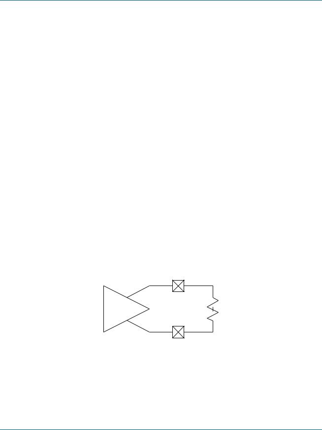
VOD |
Output Differential Voltage, |
Figure 4 |
|
240 |
325 |
420 |
mV |
|
||
|
pad_ChX_p - Pad_ChX_n |
|
|
||||||||
|
Figure 5 |
|
|
||||||||
|
|
|
|
|
|
|
|
|
|
|
|
|
|
|
RL = 27Ω |
|
|
|
|
|
|
|
|
|
VOS |
Offset Voltage |
|
0.90 |
1.10 |
1.30 |
V |
|
|||
|
|
|
DO = 0 V, |
|
|
|
|
|
|
|
|
|
IOS |
Output Short Circuit Current |
DIN + H, |
|
20 |
25 |
35 |
mA |
|
||
|
|
|
EN + OE + VCC |
|
|
|
|
|
|
|
|
|
IOZ |
Tri-State Output Current |
DO = 0 V/VCC, |
|
-25 |
±10 |
25 |
µA |
|
||
|
EN = 0 |
|
|
||||||||
|
IOX |
Power-Off Output Current |
VCC - 0 V, |
|
-25 |
±10 |
25 |
µA |
|
||
|
DO = 0 V/VCC |
|
|
||||||||
|
|
|
|
|
|
|
|
|
|
|
|
|
|
Table 11: Deserializer / Receiver |
|
|
|
|
|
|
|
||
|
|
|
|
|
|
|
|
|
|
|
|
|
Symbol |
Parameter |
Conditions |
Min |
|
Typ |
|
Max |
Units |
|
|
|
|
|
|
|
|
|
|
|
|
|
|
|
VTH |
Differential Threshold High Voltage |
Figure 6 |
n/a |
|
35 |
|
50 |
mV |
|
|
|
|
|
VCM = 1.1 V |
|
|
|
|
|
|
|
|
|
VTL |
Differential Threshold Low Voltage |
-50 |
|
-35 |
|
n/a |
mV |
|
||
|
|
|
VIN = 0 V, |
-25 |
|
±8 |
|
25 |
µA |
|
|
|
IIN |
Input Current |
VCC = 0 V / 3.6 V |
|
|
|
|
|
|
|
|
|
VIN = 2.4 V, |
-25 |
|
±8 |
|
25 |
µA |
|
|||
|
|
|
|
|
|
||||||
|
|
|
VCC = 0 V / 3.6 V |
|
|
|
|
|
|
|
|
D out +
D out -
Figure 4: Output Differential Voltage
© 2002 QuickLogic Corporation
Preliminary
•
www.quicklogic.com •
•• 9
•
•
QL82SD Device Data Sheet Rev C
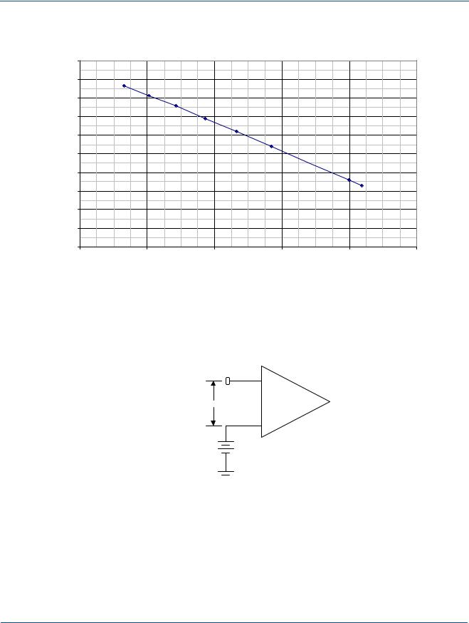
82SD BLVDS output Vod vs Iod
Vod ( v )
1.00
0.90100 Ω
0.80 |
80 Ω |
|
|
0.70 |
|
60 Ω
0.60
0.50
 40 Ω
40 Ω
0.40
27 Ω
0.30
0.20
0.10
0.00
8 |
9 |
10 |
11 |
12 |
13 |
Iod ( mA )
Figure 5: Output Differential Voltage for Different Loads
VTH/ VTL
VCM
Figure 6: Differential Threshold Voltages
•
•
10 •• www.quicklogic.com Preliminary © 2002 QuickLogic Corporation
•
•
QL82SD Device Data Sheet Rev C
Supply Current per Channel
Table 12: Serializer / Transmitter
|
Symbol |
Parameter |
|
|
Conditions |
|
Min |
|
Typ |
|
Max |
Units |
|
|||
|
|
|
|
|
|
|
|
|
|
|
|
|
|
|
|
|
|
|
|
|
|
|
Figure 7 |
1:1 Mode |
|
|
Figure 7 |
|
|
mA |
|||
|
|
|
|
|
|
|
|
|
|
|
|
|
|
|
|
|
|
|
|
|
|
|
Figure 8 |
4:1 Mode |
|
|
Figure 8 |
|
|
mA |
|
||
|
|
|
|
|
|
|
|
|
|
|
|
|
|
|
|
|
|
ICCT |
Serializer Supply Current |
|
CL =10 pF |
Figure 9 |
7:1 Mode |
|
|
Figure 9 |
|
|
mA |
||||
|
|
|
|
|
|
|
|
|
|
|
|
|
||||
|
|
Figure 12 |
8:1 Mode |
|
|
Figure 12 |
|
|
mA |
|
||||||
|
|
|
|
|
|
|
|
|
|
|
||||||
|
|
|
|
|
|
|
|
|
|
|
|
|
|
|
|
|
|
|
|
|
|
|
Figure 11 |
10:1 Mode |
|
|
Figure 11 |
|
|
mA |
|||
|
|
|
|
|
|
Data/Clock |
|
|
|
|
||||||
|
|
|
|
|
|
|
|
|
|
|
|
|
|
|
|
|
|
|
|
|
|
|
|
|
|
|
|
|
|
|
|
|
|
|
ICCTX |
Serializer Supply Current |
|
|
EN = 0 |
|
|
1 |
|
10 |
|
µA |
|
|||
|
Powerdown |
|
|
|
|
|
|
|
||||||||
|
|
|
|
Table 13: Deserializer / Receiver |
|
|
|
|
|
|
|
|
|
|||
|
|
|
|
|
|
|
|
|
|
|
|
|
|
|
||
Symbol |
|
Parameter |
|
|
Conditions |
|
Min |
|
Typ |
Max |
|
Units |
||||
|
|
|
|
|
|
|
|
|
|
|
|
|
|
|
|
|
|
|
|
|
|
|
Figure 13 |
1:1 Mode |
|
|
|
Figure 13 |
|
|
mA |
||
|
|
|
|
|
|
|
|
|
|
|
|
|
|
|
|
|
|
|
|
|
|
|
Figure 14 |
4:1 Mode |
|
|
|
Figure 14 |
|
|
mA |
||
|
|
|
|
|
|
|
|
|
|
|
|
|
|
|
|
|
|
ICCR |
|
Serializer Supply Current |
CL = 10 pF |
Figure 15 |
7:1 Mode |
|
|
|
Figure 15 |
|
|
mA |
|||
|
|
|
|
|
|
|
|
|
|
|
|
|
||||
|
|
Figure 13 |
8:1 Mode |
|
|
|
Figure 13 |
|
|
mA |
||||||
|
|
|
|
|
|
|
|
|
|
|
||||||
|
|
|
|
|
|
|
|
|
|
|
|
|
|
|
|
|
|
|
|
|
|
|
Figure 14 |
10:1 Mode |
|
|
|
Figure 14 |
|
|
mA |
||
|
|
|
|
|
|
Data/Clock |
|
|
|
|
|
|||||
|
|
|
|
|
|
|
|
|
|
|
|
|
|
|
|
|
|
|
|
|
|
|
|
|
|
|
|
|
|
|
|
|
|
|
ICCRX |
|
Serializer Supply Current |
|
|
EN = 0 |
|
|
|
1 |
|
10 |
|
µA |
||
|
|
Powerdown |
|
|
|
|
|
|
|
|||||||
NOTE: More accurate supply current/power consumption numbers specific to your application should be calculated using the power calculator supplied with QuickLogic’s QuickWorks software package.
© 2002 QuickLogic Corporation
Preliminary
•
www.quicklogic.com •
•• 11
•
•

QL82SD Device Data Sheet Rev C
Supply Current at VccTx = 2.5 V
|
13 |
|
|
|
|
|
|
|
|
|
|
12 |
|
|
|
|
|
|
|
|
|
(mA) |
11 |
|
|
|
|
|
|
|
|
|
|
|
|
|
|
|
|
|
|
|
|
ICCT |
10 |
|
|
|
|
|
|
|
|
|
|
|
|
|
|
|
|
|
|
|
|
|
9 |
|
|
|
|
|
|
|
|
|
|
|
|
|
|
|
|
|
|
|
|
|
|
|
|
|
|
|
Rt=100ohm |
|||
|
0 |
|
|
|
|
|
|
Rt= 27ohm |
|
|
|
|
|
|
|
|
|
|
|
|
|
|
0 |
100 |
200 |
300 |
400 |
500 |
600 |
700 |
||
Clock Frequency(MHz)
Figure 7: Data/Clock Channel, 1:1 Transmit Mode
Supply Current at VccTx = 2.5 V
20
(mA) |
15 |
|
|
|
|
|
|
|
|
ICCT |
|
|
|
|
|
|
|
|
|
|
|
|
|
|
|
|
|
|
|
|
|
|
|
|
|
|
|
|
|
|
10 |
|
|
|
|
|
Rt=100ohm |
||
|
|
|
|
|
|
Rt= 27ohm |
|
||
|
20 |
40 |
60 |
80 |
100 |
120 |
|
|
|
|
140 |
160 |
|||||||
|
|
|
Clock Frequency(MHz) |
|
|
|
|||
Figure 8: Data/Clock Channel, 4:1 Transmit Mode
Supply Current at VccTx = 2.5V
25
|
20 |
|
|
|
|
ICCT (mA) |
15 |
|
|
|
|
|
|
|
|
|
|
|
|
|
|
|
Rt=100ohm |
|
10 |
|
|
|
Rt= 27ohm |
|
|
|
|
|
|
|
30 |
50 |
70 |
90 |
|
|
10 |
Clock Frequency(MHz)
Figure 9: Data/Clock Channel, 7:1 Transmit Mode
Supply Current at VccTx = 2.5 V
25
|
20 |
|
|
|
|
|
|
ICCT (mA) |
15 |
|
|
|
|
|
|
|
|
|
|
|
|
|
|
|
|
|
|
Rt=100ohm |
|||
|
10 |
|
|
|
Rt= 27ohm |
|
|
|
30 |
50 |
70 |
|
|
||
|
10 |
|
|
||||
|
|
Clock Frequency(MHz) |
|
|
|
|
|
Figure 10: Data/Clock Channel, 8:1 Transmit Mode |
|||||||
|
25 |
Supply Current at VccTx = 2.5 V |
|||||
|
|
|
|
|
|
|
|
|
20 |
|
|
|
|
|
|
ICCT (mA) |
15 |
|
|
|
|
|
|
|
|
|
|
|
|
|
|
|
|
|
|
Rt=100ohm |
|||
|
10 |
|
|
|
Rt= 27ohm |
|
|
|
|
40 |
60 |
|
|
|
|
|
|
|
|
|
|||
|
20 |
|
|
|
|
||
Clock Frequency(MHz)
Figure 11: Data/Clock Channel,10:1 Transmit Mode
20Supply Current at VCCRX = 3.3 V VCC = 2.5 V
|
18 |
|
|
|
|
|
|
|
|
16 |
|
|
|
|
|
|
|
(mA) |
14 |
|
|
|
|
|
|
|
12 |
|
|
|
|
|
|
|
|
|
|
|
|
|
|
|
|
|
ICCR |
10 |
|
|
|
|
|
|
|
8 |
|
|
|
|
|
|
|
|
|
6 |
|
|
|
|
|
|
|
|
4 |
|
|
|
|
|
|
|
|
2 0 |
100 |
200 |
300 |
400 |
500 |
600 |
700 |
|
|
|
Clock Frequency (MHz) |
|
|
|||
Figure 12: Data/Clock Channel, 1:1 Receive Mode
•
•
12 •• www.quicklogic.com Preliminary © 2002 QuickLogic Corporation
•
•
Supply Current at VCCRX = 3.3 V, VCC = 2.5 V
25
|
20 |
|
|
|
|
|
|
|
(mA) |
15 |
|
|
|
|
|
|
|
ICCR |
|
|
|
|
|
|
|
|
|
10 |
|
|
|
|
|
|
|
|
5 |
40 |
60 |
80 |
100 |
120 |
140 |
160 |
|
20 |
|||||||
|
|
|
Clock Frequency (MHz) |
|
|
|
||
Figure 13: Data/Clock Channel, 4:1 Receive Mode |
||||||||
|
Supply Current at VCCRX = 3.3 V, VCC = 2.5 V |
|||||||
|
20 |
|
|
|
|
|
|
|
|
15 |
|
|
|
|
|
|
|
(mA) |
10 |
|
|
|
|
|
|
|
ICCR |
|
|
|
|
|
|
|
|
|
|
|
|
|
|
|
|
|
|
5 |
|
|
|
|
|
|
|
|
0 |
|
|
|
|
|
|
|
|
10 |
|
30 |
50 |
70 |
90 |
|
|
|
|
|
Clock Frequency (MHz) |
|
|
|
||
Figure 14: Data/Clock Channel, 7:1 Receive Mode
QL82SD Device Data Sheet Rev C
20 Supply Current at VCCRX = 3.3 V, VCC = 2.5 V
|
15 |
|
|
|
|
|
|
|
|
|
(mA) |
|
|
|
|
|
|
|
|
|
|
ICCR |
10 |
|
|
|
|
|
|
|
|
|
|
|
|
|
|
|
|
|
|
|
|
|
5 |
|
|
|
|
|
|
|
|
|
|
0 |
|
|
|
|
|
|
|
|
|
|
10 |
20 |
30 |
40 |
50 |
|
60 |
70 |
80 |
90 |
|
|
|
Clock Frequency (MHz) |
|
|
|||||
Figure 15: Data/Clock Channel, 8:1 Receive Mode |
||||||||||
|
20 Supply Current at VCCRX = 3.3 V, VCC = 2.5 V |
|||||||||
|
15 |
|
|
|
|
|
|
|
|
|
(mA) |
10 |
|
|
|
|
|
|
|
|
|
ICCR |
|
|
|
|
|
|
|
|
|
|
|
5 |
|
|
|
|
|
|
|
|
|
|
0 |
25 |
30 |
35 |
40 |
45 |
50 |
55 |
60 |
70 |
|
20 |
|||||||||
Clock Frequency (MHz)
Figure 16: Data/Clock Channel, 10:1 Receive Mode
© 2002 QuickLogic Corporation
Preliminary
•
www.quicklogic.com •
•• 13
•
•
QL82SD Device Data Sheet Rev C
SERDES Timing Requirements
NOTE: Both Table 14 and Table 15 refer to CDR (10:1) Mode for ChX_txclk and Channel Link (8:1, 7:1, 4:1) Mode for ClkX_txclk
Table 14: Serializer / Transmitter Transmit Clock
Symbol |
Parameter |
Conditions |
Min |
Typ |
Max |
Units |
|
|
|
|
|
|
|
tTCP |
Transmit Clock Period |
Mode |
n/a |
T |
n/a |
nS |
Dependent |
||||||
tTDC |
Transmit Clock Duty Cycle |
|
45 |
50 |
55 |
% |
tCLKT |
Transmit Clock Input Transition Time |
Figure 17 |
1 |
n/a |
n/a |
V/nS |
tJIT |
Transmit Clock Input Jitter |
|
n/a |
n/a |
150.0 |
pS |
|
(RMS) |
|||||
|
Table 15: Deserializer / Receiver Transmit Clock |
|
|
|
||
|
|
|
|
|
|
|
Symbol |
Parameter |
Conditions |
Min |
Typ |
Max |
Units |
|
|
|
|
|
|
|
tRFCP |
Reference Clock Period |
Mode |
n/a |
T |
n/a |
nS |
Dependent |
||||||
tRFDC |
Reference Clock Duty Cycle |
|
40 |
50 |
60 |
% |
tRFCP/tTCP |
Ratio of Reference Clock to |
|
0.4 |
0.5 |
0.6 |
n/a |
Transmit Clock |
|
|||||
tRFTT |
Reference Clock Transition Time |
Figure 17 |
1 |
n/a |
n/a |
V/nS |
|
90% |
|
|
|
|
|
|
|
|
90% |
|
||||||
|
|
|
|
|
|
|
|
|
|||||||||
txclk |
10% |
|
|
|
|
|
|
|
|
|
|
|
|
10% |
|||
|
|
|
|
|
|
|
|
|
|
|
|
||||||
|
|
|
|
|
|
|
|
|
|
|
|
||||||
|
|
|
|
|
|
|
|
|
|
|
|
|
|
|
|
|
|
|
|
|
|
|
|
|
|
|
|
|
|
|
|
|
|
|
|
|
|
|
|
|
|
|
|
|
|
|
|
|
|
|
|
|
|
tclkT/tRFTT tclkT/tRFTT
Figure 17: Serializer Transmit Clock / Deserializer Reference Clock Transition Times
•
•
14 •• www.quicklogic.com Preliminary © 2002 QuickLogic Corporation
•
•

QL82SD Device Data Sheet Rev C
SERDES Switching Characteristics - Serializer/Transmitter]
Table 16: Serializer/Transmitter Switching Characteristics
|
|
|
CDR (10:1) Mode |
|
|
|
|
|
|
|||
Symbol |
|
Parameter |
|
Conditions |
|
Min |
|
Typ |
|
Max |
|
Units |
|
|
|
|
|
|
|||||||
|
|
|
|
|
|
|
|
|
|
|
|
|
tHZD |
|
pad_ChX_p/n High to Tri-State Delay |
|
|
|
1.9 |
|
2.2 |
|
2.5 |
|
nS |
tLZD |
|
pad_ChX_p/n Low to Tri-State Delay |
|
Figure 18 |
|
1.9 |
|
2.0 |
|
2.2 |
|
nS |
tZHD |
|
pad_ChX_p/n Tri-State to High Delay |
|
|
1.9 |
|
2.4 |
|
3.0 |
|
nS |
|
|
|
|
|
|
|
|
||||||
tZLD |
|
pad_ChX_p/n Tri-State to Low Delay |
|
|
|
2.0 |
|
2.3 |
|
2.8 |
|
nS |
tDIS |
|
ChX_txd[9:0] Setup to ChX_txclk |
|
Figure 19 |
|
2.6 |
|
|
|
3.2 |
|
nS |
tDIH |
|
ChX_txd[9:0] Hold from ChX_txclk |
|
|
|
2.1 |
|
|
|
2.7 |
|
nS |
tPLD |
|
Serializer PLL Lock Time |
|
Figure 20 |
|
|
|
|
|
90 |
|
uS |
|
|
Channel Link (8:1, 7:1, 4:1) Mode |
|
|
|
|
|
|
||||
|
|
|
|
|
|
|
|
|
|
|
|
|
Symbol |
|
Parameter |
|
Conditions |
|
Min |
|
Typ |
|
Max |
|
Units |
|
|
|
|
|
|
|
|
|
|
|
|
|
tHZD |
|
pad_ChX_p/n High to Tri-State Delay |
|
|
|
1.9 |
|
2.2 |
|
2.5 |
|
nS |
tLZD |
|
pad_ChX_p/n Low to Tri-State Delay |
|
Figure 18 |
|
1.9 |
|
2.0 |
|
2.2 |
|
nS |
tZHD |
|
pad_ChX_p/n Tri-State to High Delay |
|
|
|
1.9 |
|
2.4 |
|
3.0 |
|
nS |
tZLD |
|
pad_ChX_p/n Tri-State to Low Delay |
|
|
|
2.0 |
|
2.3 |
|
2.8 |
|
nS |
tDIS |
|
ChX_txd[N-1:0] Setup to ChX_txclk |
|
|
|
2.6 |
|
|
|
3.2 |
|
nS |
tDIH |
|
ChX_txd[N-1:0] Hold from ChX_txclk |
|
|
|
2.1 |
|
|
|
2.7 |
|
nS |
tSD |
|
Serializer Delay |
|
Figure 21 |
|
|
|
|
|
1.7 |
|
nS |
tSCP |
|
Serial Transmit Clock Period |
|
|
|
|
|
T/mode |
|
|
|
nS |
tTXD[N-1] |
|
Transmitter Output Pulse Position for |
|
|
|
[N-1] x tSCP + 1.1 |
|
|
|
[N-1] x tSCP + 1.5 |
|
nS |
|
Bit [N-1] |
|
|
|
|
|
|
|
||||
tPLD |
|
Serializer PLL Lock Time |
|
Figure 20 |
|
|
|
|
|
90 |
|
uS |
|
|
Asynchronous Level Conversion (1:1) Mode |
|
|
|
|
|
|
||||
|
|
|
|
|
|
|
|
|
|
|
|
|
tHZD |
|
pad_ChX_p/n High to Tri-State Delay |
|
|
|
1.9 |
|
2.2 |
|
2.5 |
|
nS |
tLZD |
|
pad_ChX_p/n Low to Tri-State Delay |
|
Figure 18 |
|
1.9 |
|
2.0 |
|
2.2 |
|
nS |
tZHD |
|
pad_ChX_p/n Tri-State to High Delay |
|
|
1.9 |
|
2.4 |
|
3.0 |
|
nS |
|
|
|
|
|
|
|
|
||||||
tZLD |
|
pad_ChX_p/n Tri-State to Low Delay |
|
|
|
2.0 |
|
2.3 |
|
2.8 |
|
nS |
tASD |
|
Asynchronous Serializer Delay - |
|
|
|
|
|
|
|
1.8 |
|
nS |
|
Data Channel |
|
Figure 22 |
|
|
|
|
|
|
|||
tASC |
|
Asynchronous Serializer Delay - |
|
|
|
|
|
|
|
1.7 |
|
nS |
|
Channel Clock |
|
|
|
|
|
|
|
|
|||
© 2002 QuickLogic Corporation
Preliminary
•
www.quicklogic.com •
•• 15
•
•
QL82SD Device Data Sheet Rev C
3V |
|
|
|
|
1.5V |
|
|
1.5V |
||
|
|
|
|
|
|
|||||
EN |
|
|
|
|
|
|
||||
|
|
|
|
|
|
|||||
0V |
|
|
|
|
|
|
|
|
|
|
|
|
|
|
|
|
|
|
|
|
|
V0H |
|
|
|
t HZD |
|
|
|
|
|
|
|
|
|
|
|
|
|
||||
|
|
|
|
|
|
|
|
|
|
|
|
|
|
t LZD |
|
|
|
50% |
|
||
Pad_p/n |
|
|
|
|
|
|
|
|||
|
|
|
|
|
|
|
|
|||
|
|
|
|
|
|
|
|
|||
|
|
|
|
|
|
|
|
|||
|
|
|
|
|
|
|
|
|
|
|
50%
V 0L
50%
t ZHD
50%
1.1V
t ZLD
1.1V
50%
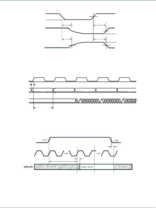
Figure 18: Serializer Delays to Tri-State
Ch0_txclk
tDIS
Ch0_txd[9:0] A |
B |
C |
D |
E |
F |
Pad_Ch0_p/n
tDIH
Figure 19: 10:1 Mode Serializer Transmit with Embedded Clock
|
|
|
|
ENABLE |
2.0V |
|
0.8V |
|
|
|
|
|
t HZD or t LZD
txclk
t ZHD or t ZLD
|
Pad_p/n |
|
TRI-STATE |
|
|
|
|
|
|
|
Output Active |
|
TRI-STATE |
||
|
|
|
|
|
|
|
|
|
|
|
|
|
|
|
|
|
|
|
|
|
|
|
|
Figure 20: Serializer PLL Times
•
•
16 •• www.quicklogic.com Preliminary © 2002 QuickLogic Corporation
•
•
QL82SD Device Data Sheet Rev C
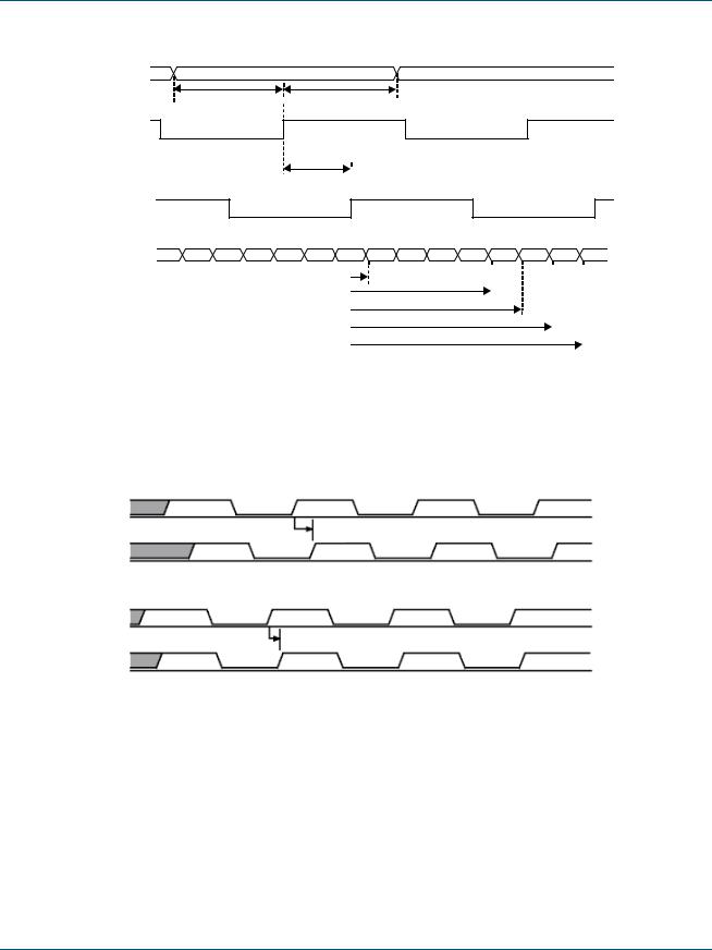
ChX _txd [7:0]
t DIS  t DIH
t DIH
ChX_txclk
|
t SD |
Pad_ClkX _p/n |
|
Pad_ ChX _p/n |
[bit3] [bit2] [bit1] [bit0] [bit7] [bit6] [bit5] [bit4] |
Note: t TXD [N-1] denotes physical bit positions wrt Pad_ClkX_p/n while Pad_ChX_p/n bit[n] refers to logical bit positions wrt ChX_txd [7:0].
t TXD [0] t TXD [4] t TXD [5] t TXD [6] t TXD [7]
Figure 21: Channel Link Mode Serializer Transmit (Using 8:1 Mode as Example)
Ch0_txd [0]
tASD
Pad_Ch0_p/n
ClkA_txclk
tASC
Pad_ClkA_p/n
Figure 22: 1:1 Mode Asynchronous Level Conversion Mode Serializer Delays
© 2002 QuickLogic Corporation
Preliminary
•
www.quicklogic.com •
•• 17
•
•

QL82SD Device Data Sheet Rev C
SERDES Switching Characteristics - Deserializer/Receiver
Table 17: Deserializer / Receiver Switch Characteristics
|
|
|
|
CDR (10:1) Mode |
|
|
|
|
|
|
|
|
|
|
|
|
||||
Symbol |
|
Parameter |
|
Conditions |
Min |
|
Typ |
|
|
|
|
Max |
|
Units |
||||||
|
|
|
|
|
|
|
|
|||||||||||||
|
|
|
|
|
|
|
|
|
|
|
|
|
|
|
|
|
|
|
|
|
tRCP |
|
ChX_rxclk Period |
|
|
28.5 |
|
|
|
|
T |
40.0 |
|
|
|
|
nS |
||||
tRDC |
|
ChX_rxclk Duty Cycle |
|
|
45 |
|
|
|
|
50 |
55 |
|
|
|
|
% |
||||
tDD |
|
Deserializer Delay |
|
Figure 23 |
2 × tRCP + 1.5 |
|
2 × tRCP + 2.5 |
|
|
|
|
2 × tRCP + 3.5 |
|
nS |
||||||
tRXPD |
|
ChX_rxclk to ChX_rxd[9..0] |
|
|
1.5 |
|
|
|
|
2.5 |
3.5 |
|
|
|
|
nS |
||||
tDSR1 |
|
Deserializer PLL Lock Time |
|
Figure 24: 25 MHz |
|
|
|
|
|
5 |
|
|
|
|
|
|
|
|
|
uS |
|
|
|
|
|
|
|
|
|
|
|
|
|
|
|
|
|
||||
|
from powered-down state |
|
Figure 24: 50 MHz |
|
|
|
|
|
8 |
|
|
|
|
|
|
|
|
|
uS |
|
|
|
|
|
|
|
|
|
|
|
|
|
|
|
|
|
|
|
|
|
|
|
|
|
|
|
|
|
|
|
|
|
|
|
|
|
|
|
|
|
|
|
tDSR2 |
|
Deserializer PLL Lock Time from SYNCPAT |
|
Figure : 25 MHz |
|
|
|
|
|
1 |
|
|
|
|
|
|
|
|
|
uS |
|
|
|
|
|
|
|
|
|
|
|
|
|
|
|
|
|
||||
|
|
Figure : 50 MHz |
|
|
|
|
|
0.75 |
|
|
|
|
|
|
|
|
|
uS |
||
|
|
|
|
|
|
|
|
|
|
|
|
|
|
|
|
|
|
|
|
|
|
|
|
|
|
|
|
|
|
|
|
|
|
|
|
|
|
|
|
|
|
tDJIT |
|
Pad_ChX_p/n Jitter |
|
25 MHz |
|
|
|
|
|
±350 |
|
|
|
|
|
|
|
|
|
pS |
|
|
50 MHz |
|
|
|
|
|
±200 |
|
|
|
|
|
|
|
|
|
pS |
||
|
|
Channel Link (8:1, 7:1, 4:1) Mode |
|
|
|
|
|
|
|
|
|
|
|
|
||||||
|
|
|
|
|
|
|
|
|
|
|
|
|
|
|
|
|
|
|
|
|
Symbol |
|
Parameter |
|
Conditions |
Min |
|
Typ |
|
|
|
|
Max |
|
Units |
||||||
|
|
|
|
|
|
|
|
|
|
|
|
|
|
|
|
|
|
|
|
|
|
|
|
|
|
Mode Dependent |
|
|
Mode Dependent |
|
|
||||||||||
tRCP |
|
|
|
|
LVDS Link |
|
-1 |
|
|
|
|
|
|
LVDS Link |
|
-1 |
|
|
||
|
|
|
|
|
|
|
|
|
|
|
|
|
|
|
||||||
|
ChX_rxclk Period |
|
|
Frequency |
|
|
|
T |
|
|
|
|
Frequency |
|
|
|
nS |
|||
|
|
|
Compression |
|
|
|
||||||||||||||
|
|
|
|
|
|
|
|
Compression |
|
|
|
|||||||||
|
|
|
|
|
Mode |
|
|
|
|
|
|
|
|
Mode |
|
|
|
|||
|
|
|
|
|
|
|
|
|
|
|
|
|
|
|
|
|
|
|
|
|
tRDC |
|
ChX_rxclk Duty Cycle |
|
|
45 |
|
|
|
|
50 |
55 |
|
|
|
|
% |
||||
tDD |
|
Deserializer Delay |
|
|
2 × tRCP + 1.5 |
|
2 × tRCP + 2.5 |
|
|
|
|
2 × tRCP + 3.5 |
|
nS |
||||||
tRXPD |
|
ChX_rxclk to ChX_rxd[N-1..0] |
|
|
1.5 |
|
|
|
|
2.5 |
3.5 |
|
|
|
|
nS |
||||
tRXDS |
|
Pad_ChX_p/n Setup to Strobe Position |
|
Figure 26 |
|
|
|
|
|
150 |
200 |
|
|
|
|
pS |
||||
tRXDH |
|
Pad_ChX_p/n Hold to Strobe Position |
|
|
|
|
|
|
|
150 |
200 |
|
|
|
|
pS |
||||
tSCD |
|
Pad_ClkX_p/n to Serial Clock Delay a |
|
|
0.6 |
|
|
|
|
0.8 |
1 |
|
|
|
|
nS |
||||
tSCP |
|
Serial Clock Period |
|
|
|
|
|
|
|
T/mode |
|
|
|
|
|
|
|
|
|
nS |
tRXD[N-1] |
|
Receiver Input Strobe Position for Bit [N-1] |
|
|
[N-1] × tSCP + 1.1 |
|
|
|
[N-1] × tSCP + 2.4 |
|
nS |
|||||||||
tDSR1 |
|
Deserializer PLL Lock Time from |
|
Figure 24: 25 MHz |
|
|
|
|
|
5 |
|
|
|
|
|
|
|
|
|
uS |
|
|
|
|
|
|
|
|
|
|
|
|
|
|
|
|
|
||||
|
powered-down state |
|
Figure 24: 50 MHz |
|
|
|
|
|
8 |
|
|
|
|
|
|
|
|
|
uS |
|
|
|
|
|
|
|
|
|
|
|
|
|
|
|
|
|
|
|
|
|
|
|
|
|
|
|
|
|
|
|
|
|
|
|
|
|
|
|
|
|
|
|
tDJIT |
|
Pad_ChX_p/n Jitter |
|
25 MHz |
|
|
|
|
|
±300 |
|
|
|
|
|
|
|
|
|
pS |
|
|
50 MHz |
|
|
|
|
|
±150 |
|
|
|
|
|
|
|
|
|
pS |
||
|
|
Asynchronous Level Conversion (1:1) Mode |
|
|
|
|
|
|
|
|
|
|
||||||||
|
|
|
|
|
|
|
|
|
|
|
|
|
|
|
|
|
|
|
|
|
tADD |
|
Asynchronous Deserializer Delay - |
|
|
|
|
|
|
|
|
1.7 |
|
|
|
|
nS |
||||
|
Data Channel |
|
Figure 27 |
|
|
|
|
|
|
|
|
|
|
|||||||
tADC |
|
Asynchronous Serializer Delay - |
|
|
0.6 |
|
|
|
|
0.8 |
1 |
|
|
|
|
nS |
||||
|
Channel Clock a |
|
|
|
|
|
|
|
|
|
|
|||||||||
a. These values include the delay resulting from application of internal compensation for data/clock skew.
•
•
18 •• www.quicklogic.com Preliminary © 2002 QuickLogic Corporation
•
•
 Loading...